Article

Considerations for Gain Selection of Feedforward Active EMI Filters

1
Department of Control and Instrumentation Engineering, Gyeongsang National University, 501 Jinjudaero, Jinju 52828, Korea
2
LG Electronics, Changwon 51554, Korea
*
Author to whom correspondence should be addressed.
Symmetry 2022, 14(9), 1826; https://doi.org/10.3390/sym14091826
Submission received: 30 July 2022 / Revised: 26 August 2022 / Accepted: 31 August 2022 / Published: 2 September 2022

Abstract

:
The reduction of the electromagnetic interference (EMI) is an important issue in the design of switching power converters. The passive EMI filter has been widely used for the reduction of the conducted EMI. The active EMI filter (AEF) has recently been considered as a useful alternate for the small sized implementation. This paper deals with an optimal design of a voltage sensing and voltage cancellation (VSVC) type feedforward AEF. The ideal feedforward AEF is theoretically stable because it does not have any feedback loop. However, some non-ideal factors such as the source and load impedances cause the unstable operation of the AEF for certain AEF gains, which limits the magnitude of the gain and degrades the performance of the AEF. In order to overcome this problem, the method of selecting the optimum AEF gain is studied with considering both the stability and AEF performance using the concept of the symmetry. The characteristics of the cancellation loop for the AEF including the source and load impedances is first investigated in view of the stability. The boundary of the maximum AEF gain to ensure the stable operation is then discussed based on the theoretic analysis and experimental works for the actual AEF. The results can be used for implementing the AEF with the optimum EMI reduction performance.

1. Introduction

The mitigation of the electromagnetic interference (EMI) effects has been considered as an important issue in the area of high frequency switching power converters. The recent wide bandgap (WBG) devices such as the SiC MOSFET and GaN HEMT make the switching transient with the high dv/dt and di/dt, and thus the importance of the EMI reduction technique is more increased in the design of the high switching power converters [1,2].
The passive filter with the common-mode (CM) choke and X- and Y-capacitors has been used for reducing the conducted emission (CE) of the EMI in most existing converter circuits [3,4,5,6,7]. The systematic design methods of the passive EMI filters were presented in [3,4,7]. The empirical approach for the boost power factor correction (PFC) converter was also found in [5]. However, the passive EMI filters inherently need bulky passive components. The passive cancellation method using the compensation winding is quite effective for several converter topologies [6], but its design process is not systematic and the application area is limited. In order to reduce the size of the passive components, the active EMI filter (AEF) has recently been considered as an alternate to the passive filter. Since the AEF employs an active cancellation of the noise currents and voltages rather than the filtering using the bulky LC components, it has a great possibility to integrate the EMI filter in a small chip or package.
Research on the analysis and design of the AEFs can be found in the literature [8,9,10,11,12,13,14,15,16,17,18,19,20,21]. The structure of the AEFs can be classified into the feedforward and feedback types by the structure of the cancellation loop [14,15,19]. The feedback AEF generally senses the AEF output or the noise voltage of the line impedance stabilization network (LISN), and the noise voltage is then minimized by the feedback control loop. However, the very high gain of the AEF is required to reduce the amount of the noise current or voltage below the meaningful level. The feedforward AEF is simple and widely used because it utilizes the direct cancellation of the noise current or voltage at the output stage of the noise source. However, because it needs the cancellation signal with the exact same shape with the noise voltage or current, the undesirable factors such as the source and load impedances make the cancellation error and moreover cause the unstable operation of the AEF for the unity gain of the feedforward cancellation path. It is, thus, very difficult to determine the optimum gain of the AEF to ensure the stable operation. In other words, the concept of symmetry is needed to determine the AEF gain.
In order to overcome this problem, this paper deals with the optimal design of the AEF with a voltage sensing and voltage cancellation (VSVC) structure. In particular, the method of selecting the optimum AEF gain by considering both the stability and noise cancellation performance is investigated and verified through the theoretical and experimental works.
This paper is organized as follows. The basic structure and equivalent circuit of the feedback and feedforward AEFs are addressed from the previous works in Section 2. The transfer function of the AEF considering the source impedance and CM choke is first derived for the stability analysis in Section 3. The optimum selection of the AEF gain to ensure the stable operation is discussed for various source and load impedances in the next sub-sections. In Section 4, the experimental works for the actual AEF are provided for several AEF gains to verify the theoretic analysis. Some discussions for the experimental results are also given. The important results are finally concluded in Section 5.

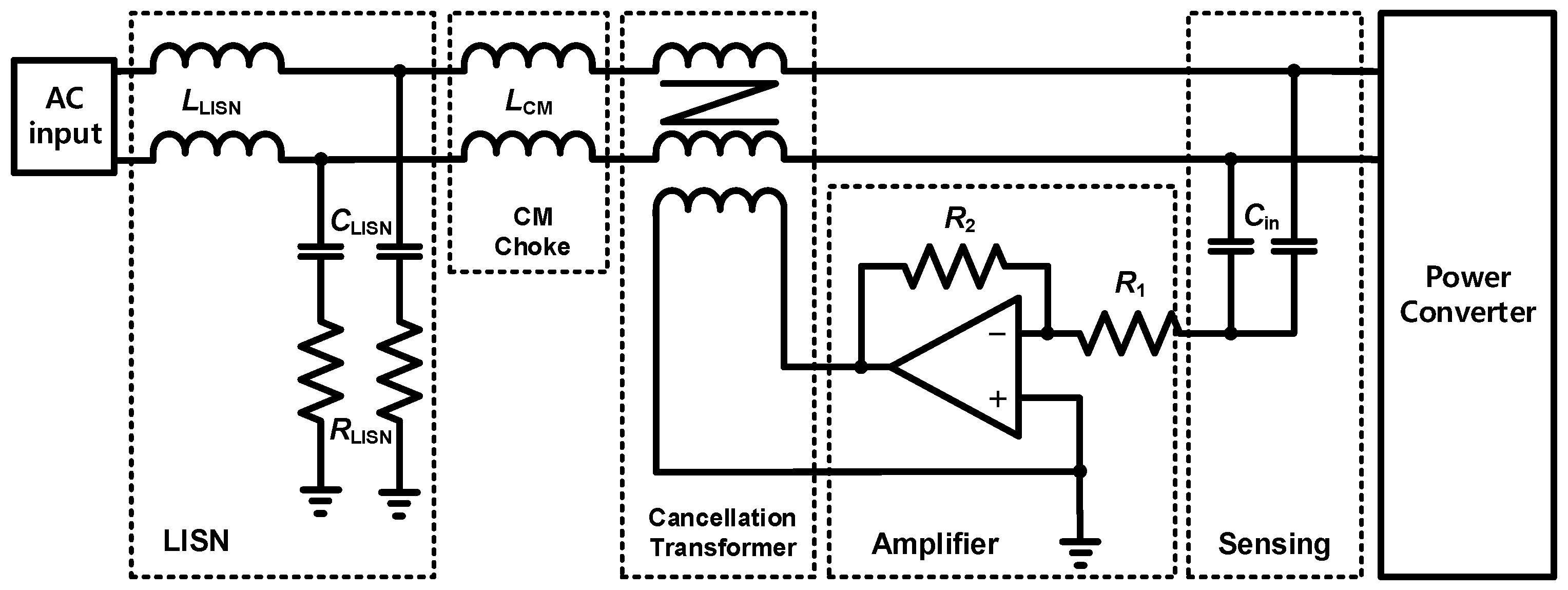
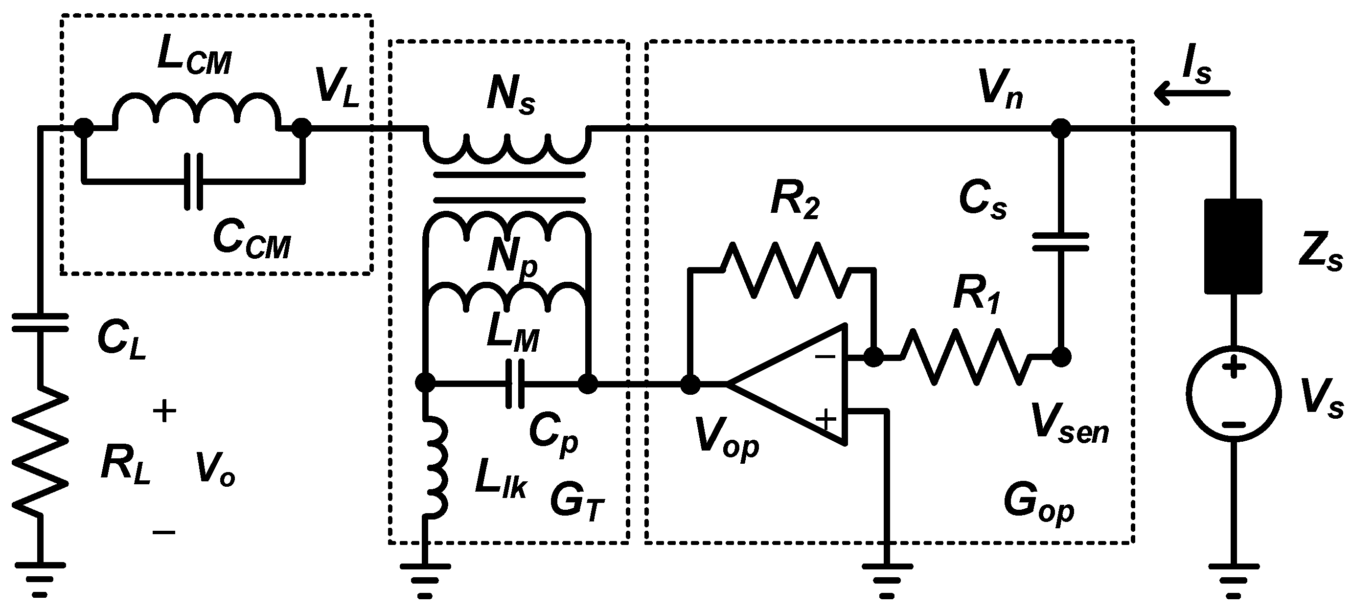
2. Structure of Active EMI Filter

There are several types of the AEFs for the sensing signals and cancellation loop structures [14,15,19]. This paper considers the VSVC-type AEF because it is simple and easy to implement [19]. The circuit for voltage sensing is simpler than for the current sensing because it can be implemented using the simple RC circuit without the additional current sensor such as the shunt and current transformer (CT). On the other hand, the high cancellation current is needed for the AEF with the current cancellation structure, and it causes the high leakage current to reach the ground, which is strictly limited by the standard regulation. Moreover, it needs a high current and high bandwidth amplifier, which is not available in practice.
Figure 1 shows the structure of the VSVC-type feedforward AEF for the common mode (CM) noise reduction, which includes the sensing circuit, control amplifier, cancellation transformer and CM choke. The noise voltage generated from the power converter is sensed at the input terminal of the power converter and is eliminated by the output of the cancellation transformer of the AEF. The noise signal measured at the terminal of the LISN becomes zero if the perfect cancellation is performed by the AEF. However, in practice, it is very difficult to make the perfect cancellation in the AEF because of the limited AEF gain to be discussed. The small CM choke (LCM) is optional for the attenuation of the high frequency noise components. It is difficult for the AEF to attenuate the noise components for entire frequency range of from 150 kHz to 30 MHz because the bandwidth of the AEF is generally below few megahertz. The LISN is not the AEF component, but the standard measuring equipment for the conducted EMI.
Two different structures of the VSVC-type AEF can also be considered for the cancellation loop structures such as the feedback and feedforward structures shown in Figure 2, where vs. and Zs denote the noise source voltage and source impedance, respectively, and the AEF is represented as the equivalent circuit including the amplifier (A), controlled voltage source (Vc), optional CM choke and LISN [14,15,19]. The noise signal is measured at the points of Vn, where the measuring points lie in the LISN terminal and power converter sides in the feedback and feedforward AEFs, respectively.
The transfer functions of the feedback and feedforward AEFs are given, respectively, as [19]
V o V s = R L Z s + ( 1 + A ) Z L
V o V s = ( 1 A ) R L ( 1 A ) Z s + Z L
where A, ZL and RL denote the transfer function of the AEF, equivalent impedance and output resistance of the LISN, respectively. It is known in (1) that the very high AEF gain is needed to make the noise voltage Vo to be zero in the feedback AEF. In contrast to the feedback AEF, the noise voltage Vo is zero when the AEF gain is unity (A = 1). The unity gain of the AEF means the AEF output is exactly the same shape with the noise signal Vn measured at the input terminal of the power converter. It is, however, very difficult to realize it in practice because of the limited bandwidth of the AEF components, source and load impedances as mentioned. Therefore, the stability and gain selection of the feedforward AEF are discussed in the next sections.

3. Considerations for Gain Selection

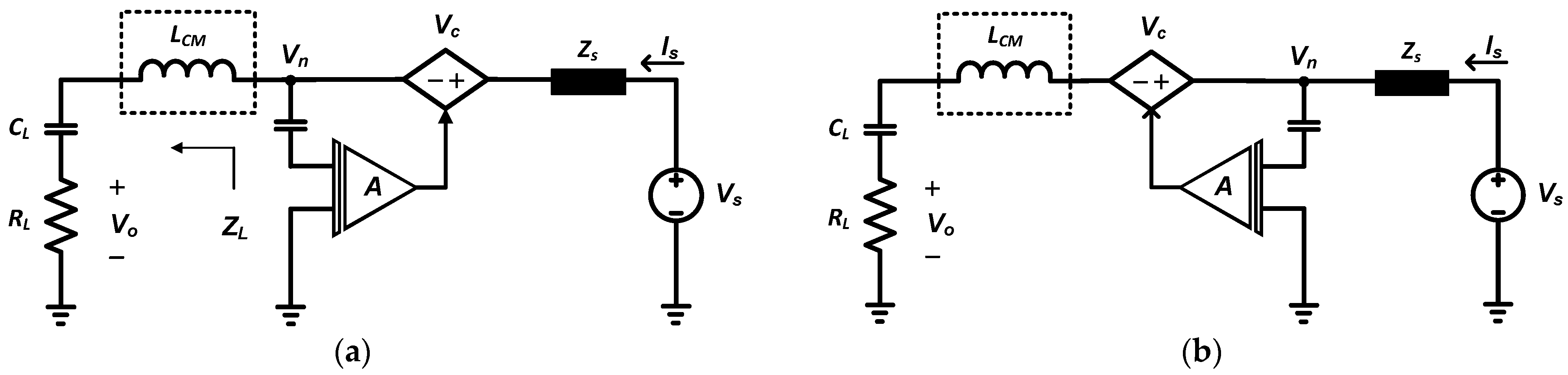
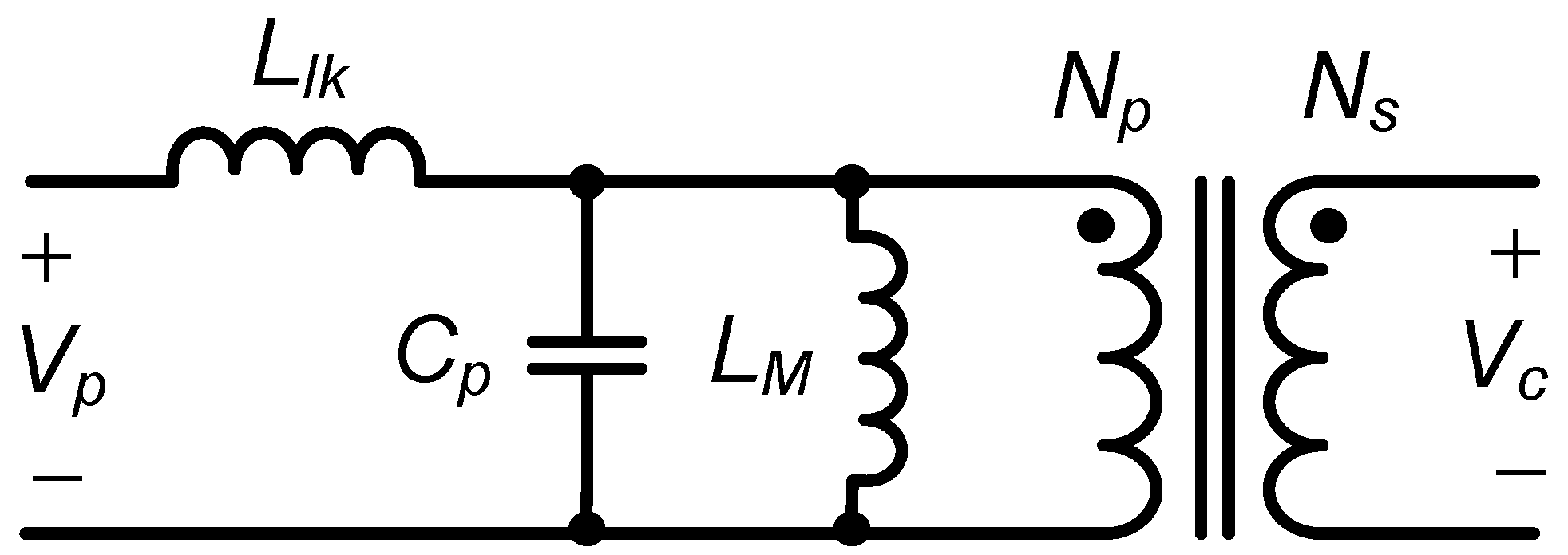
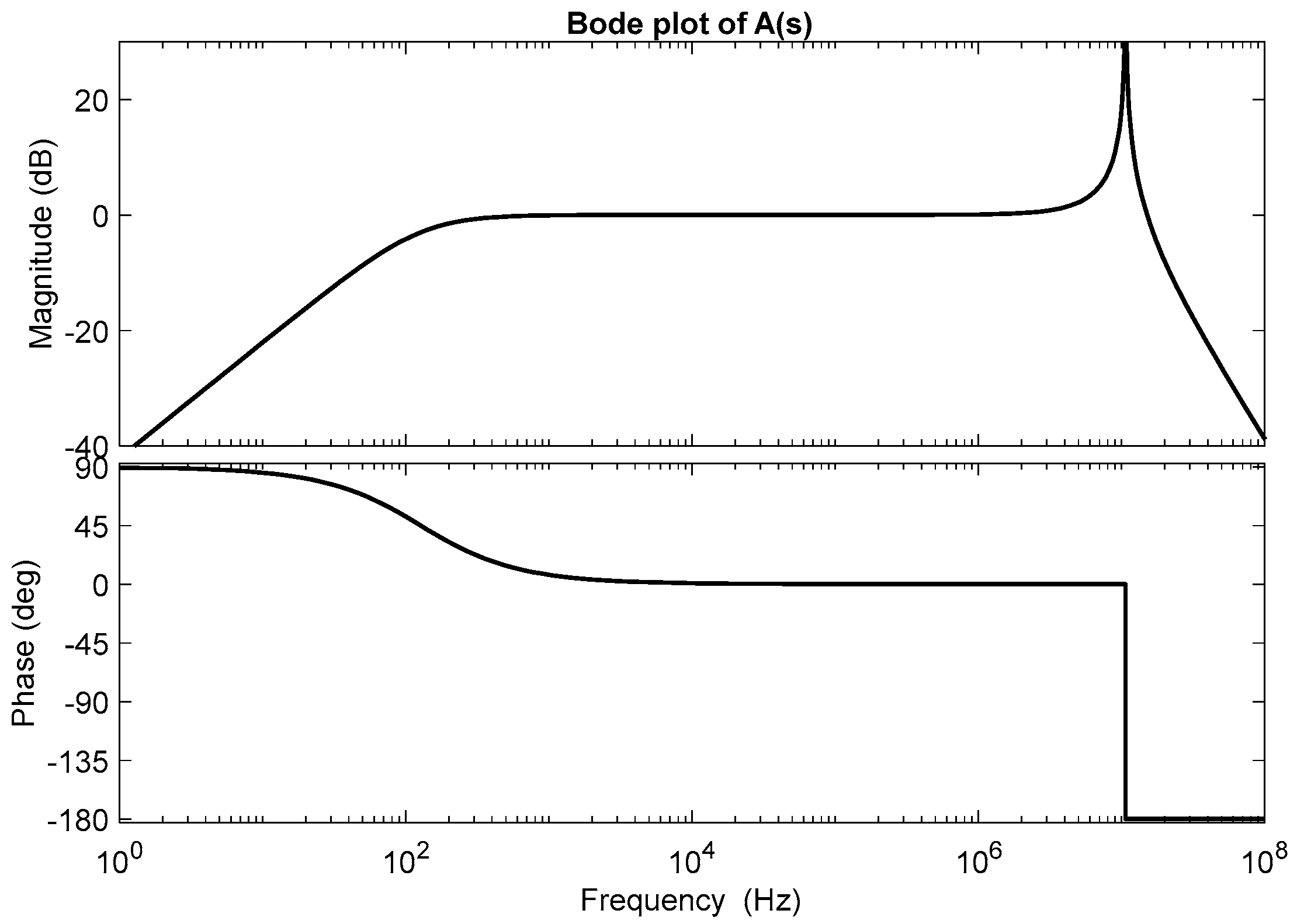
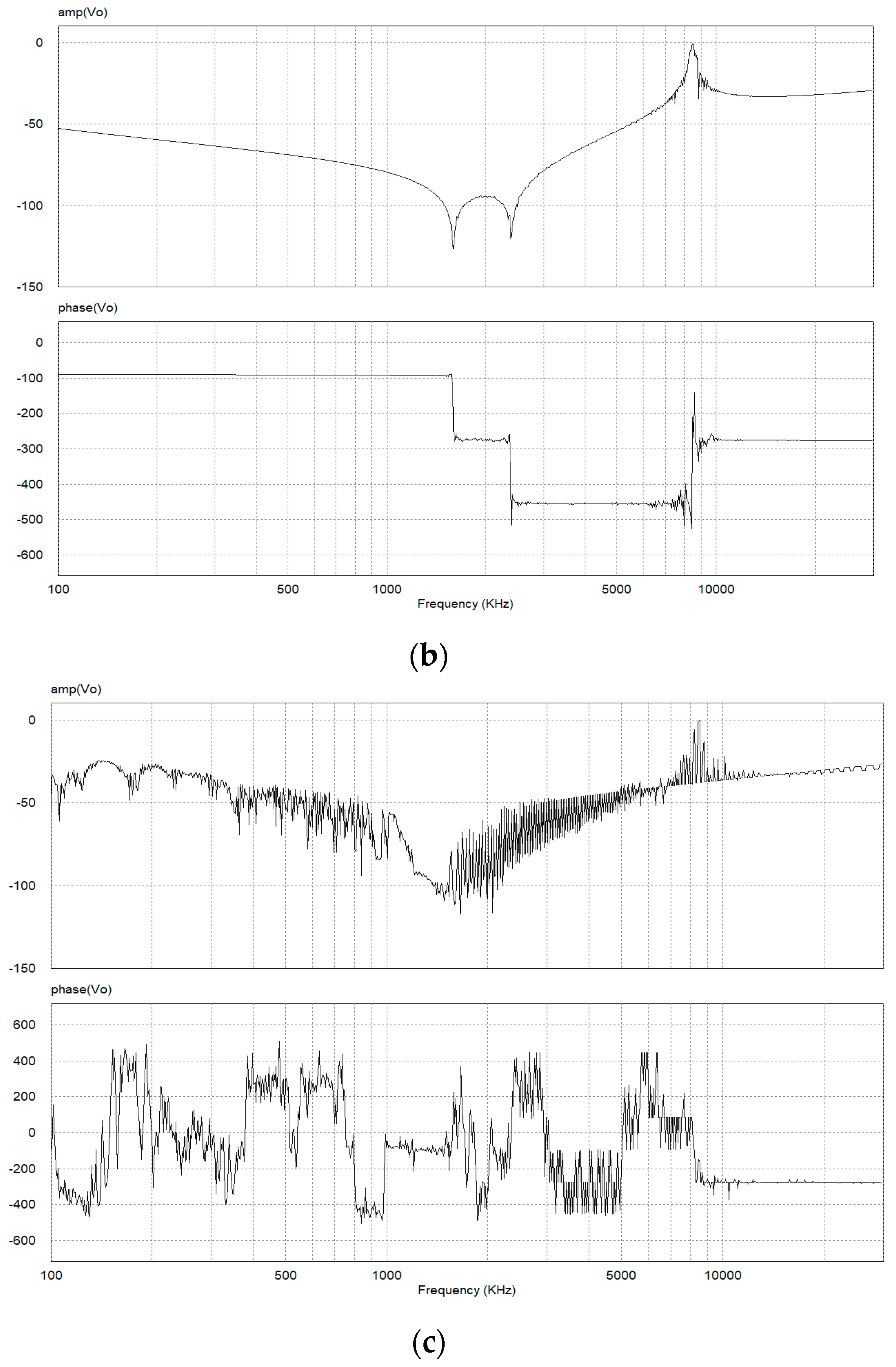
3.1. Transfer Function of Feedforward AEF

Figure 3 shows the detailed CM equivalent circuit of the VSVC-type feedforward AEF, where the AEF consists of the operational amplifier circuit and cancellation transformer.
The AEF gain is determined from this figure as
A ( s ) = V c ( s ) V n ( s ) = G o p ( s ) G T ( s )
where Gop(s) and GT(s) are the transfer functions of the operational amplifier circuit and cancellation transformer, respectively. The transfer function Gop(s) can be represented as the cascade connection of the high-pass filter and inverting amplifier as
G o p ( s ) = V p ( s ) V n ( s ) = ( s s + 2 π f h ) K o p = G h ( s ) K o p
where fh denotes the cut-off frequency of the high-pass filter and Kop is the gain of the inverting amplifier defined as
f h = 1 2 π R 1 C s
K o p = R 2 R 1
The circuit model of the cancellation transformer can be described as the second-order network, as shown in Figure 4, where Llk, LM, and Cp denote the leakage and magnetizing inductances and equivalent capacitance referred to the primary terminal, respectively. The transfer function of the cancellation transformer is represented for the condition, LM >> Llk, as [19]
G T ( s ) = V c ( s ) V p ( s ) = N s N p ( L M L M + L l k ) ( ω T 2 s 2 + ω T 2 ) n ( ω T 2 s 2 + ω T 2 )
where
n = N s N p
ω T = 1 ( L l k | | L M ) C p 1 L l k C p
The effective impedance ZL including the small CM choke is represented as
Z L = Z C M + 1 s C L + R L
where
Z C M = 1 C C M s s 2 + 1 L C M C C M
The gain of the AEF can be rewritten using (3), (4) and (7) as
A ( s ) = K f ( s s + 2 π f h ) ( ω T 2 s 2 + ω T 2 )
where the DC gain Kf is given as the multiplication of the inverting amplifier gain and turns ratio of the cancellation transformer, Kf = Kop·n. The frequency responses of the typical AEF gain A(s) and cancelled output 1 − A(s) for Kf = 1 are shown in Figure 5 and Figure 6, respectively, where the parameters of the inverting amplifier and cancellation transformer are given in Table 1. The DC gain Kf is adjusted by the value of the feedback resistor R2 and can be set as R2 = 5 kΩ for Kf = 1. The AEF gain A(s) has band-pass characteristics as shown in Figure 5. Theoretically, the noise voltage is cancelled and becomes zero if the AEF gain A(s) = 1. It is shown in Figure 6 that the noise voltage is attenuated over 20 dB for the range from 2 kHz to 3 MHz. However, in practice, the selecting the unity AEF can cause the unstable operation in certain operating conditions.

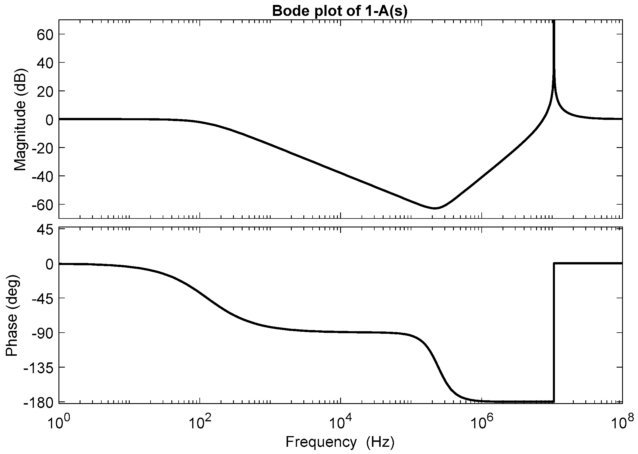
3.2. Stability Problem for the Unity AEF Gain

The transfer function between the noise source vs. and the noise voltage VL after filtering in Figure 3 can be derived from (2) and (3) as
V L ( s ) V s ( s ) = G ( s ) 1 + G ( s ) H ( s )
where
G ( s ) = 1 A ( s )
H ( s ) = Z s Z L
It is noted in (13) that the feedforward AEF has a feedback loop with a forward gain G(s) and feedback gain H(s). As shown in this equation, the characteristics of the feedforward AEF are affected by the source and load impedances, Zs and ZL. Although the performance of the AEF only is determined by the transfer function given in (13), the level of the noise voltage is measured at the terminal of the LISN. The ratio of the noise attenuation measured at the LISN terminal can be also rewritten from (13) as
V o ( s ) V s ( s ) = G ( s ) 1 + G ( s ) H ( s ) R L Z L
Since the input impedance of the power converter is generally capacitive, it is assumed that the source impedance is capacitive and is represented as
Z s = 1 s C i n
The parameters of the source and load impedances used in the analysis and experiments are given in Table 2.
The stability of the AEF for the DC gain can be investigated using the loop gain G(s)H(s) given from (13) as
G ( s ) H ( s ) = ( s 3 + 2 π f h s 2 + ( 1 K f ) ω T 2 s + 2 π f h ω T 2 s 3 + 2 π f h s 2 + ω T 2 s + 2 π f h ω T 2 ) ( Z s Z L )
where it is noted that the loop gain G(s)H(s) is a function of the DC gain Kf. The Bode plot technique is useful for this investigation, and the gain and phase margins show the relative stability of the AEF. Figure 7 shows the Bode plot of the loop gain G(s)H(s) for three different values of the DC gains Kf. It is shown in this figure that the feedforward AEF is unstable when the DC gain Kf is greater than 0.97 for the parameters given in Table 1 and Table 2. The gain and phase margins of the loop gain G(s)H(s) are 1.95 dB and 7.03 degree, respectively, for Kf = 0.94. However, these margins are decreased as the DC gain Kf increases toward the unity, and change to the negative values near Kf = 0.97. The gain and phase margins for Kf = 1 are −1.93 dB and −20.4 degree, respectively, as shown in Figure 7c. This means that the unity AEF gain (Kf = 1) to perfectly cancel the noise voltage cannot be applied in practice because of the stability problem.
Since the feedback loop in the feedforward AEF is made by the feedback gain H(s) = Zs/ZL as shown in (13), the source and load impedances can be considered as the major factors related to the stability of the feedforward AEF. Therefore, the effects of the source and load impedances on the stability of the AEF should be considered in the selection of the AEF gain and are discussed in next sections.

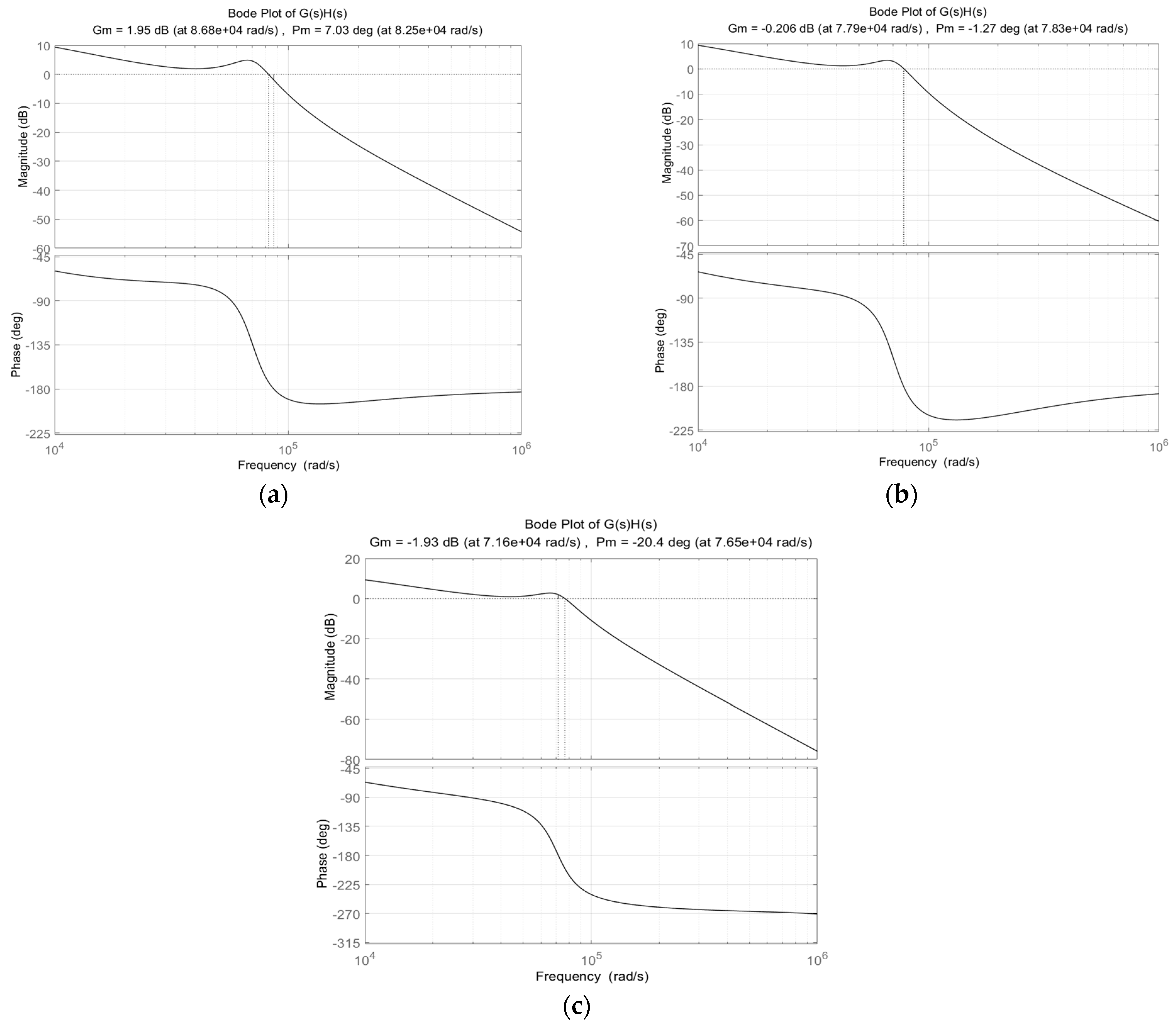
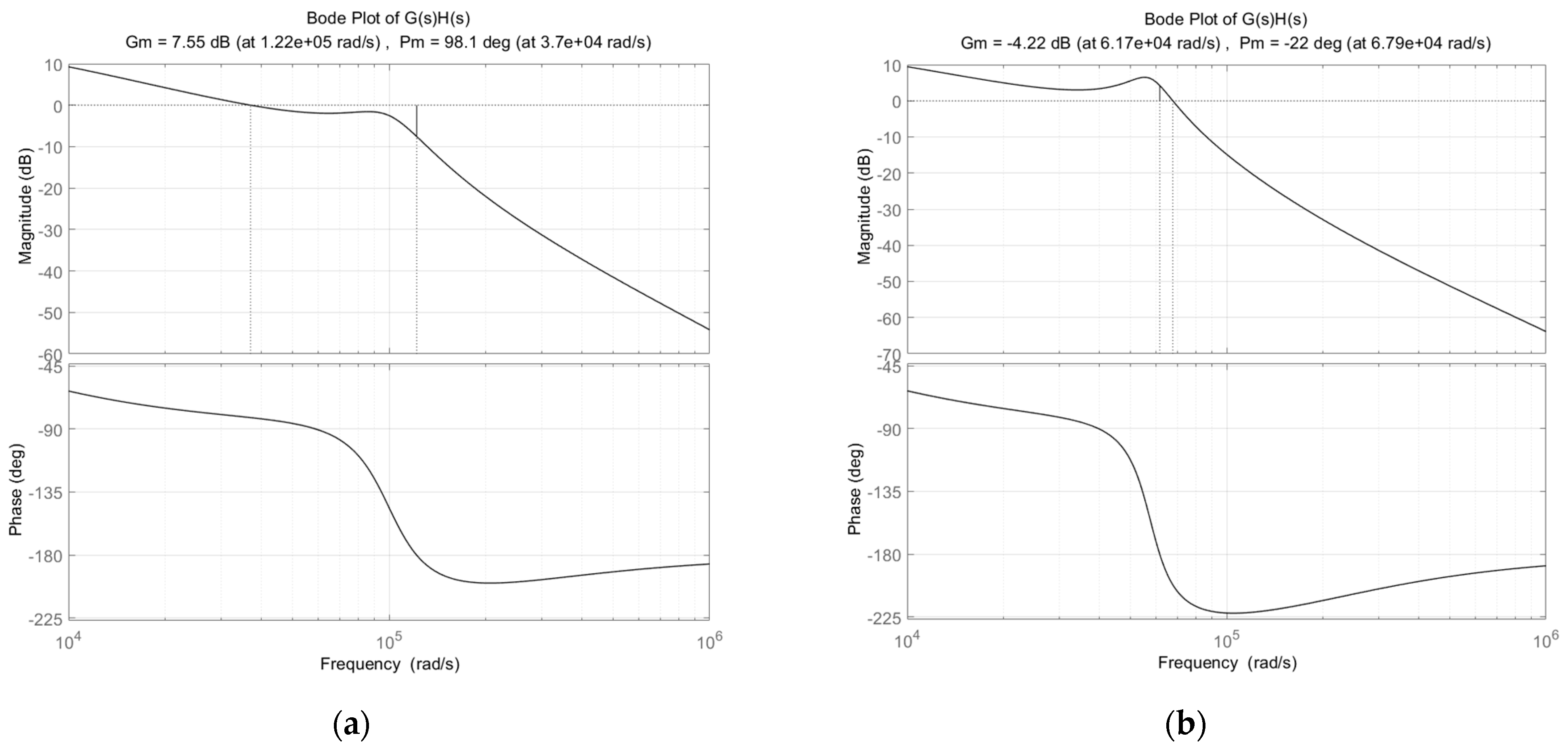
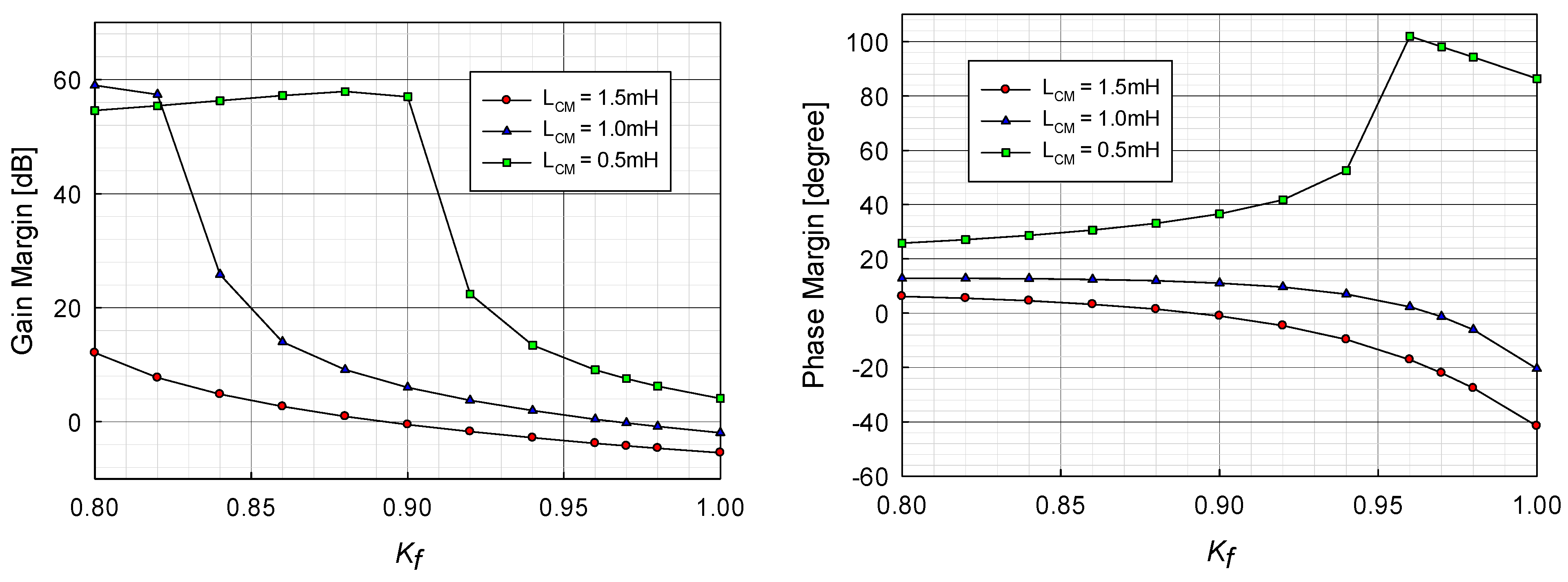
3.3. Effects of Source and Load Impedances for Stability of AEF

In order to investigate the effect of the source impedance to the AEF stability, the Bode plot analysis for the loop gain G(s)H(s) is performed for various source impedances. Figure 8 shows the gain and phase margins of the loop gain G(s)H(s) for the source capacitances Cin = 15 nF and 45 nF, respectively, and Kf = 0.97, where the other parameters are the same with the values given in Table 1 and Table 2. As shown in this figure, the gain and phase margins are 3 dB and 35.1 degree for Cin = 45 nF, and are −6.54 dB and −24.3 degree for Cin = 15 nF, respectively. It is shown in this figure that the lower source impedance (higher value of Cin) can provide the larger gain and phase margins of the AEF.
Figure 9 shows the gain and phase margins of the AEF for the different input impedances. It is shown in this figure that the phase margin is zero at the DC gain Kf = 0.9 for Cin = 15nF and this DC gain is theoretically maximum to be applied to the AEF for this value of the input impedance, whereas the maximum applicable DC gain can be increased as the source capacitance Cin increases. It is noted in this result that the low source impedance is needed to ensure the stable operation of the AEF for a wide range of Kf values.
The load impedance including the impedance of the CM choke is also an important factor that should be considered in the gain selection of the feedforward AEF. The small CM choke is effective to attenuate the noise voltage to the desired level in practice because the AEF cannot fully eliminate the noise voltage in the entire frequency range of 150 kHz to 30 MHz required for the conducted emission test. Figure 10 shows the gain and phase margins of the loop gain G(s)H(s) for the inductances of the CM choke of LCM = 0.5 mH and 1.5 mH, respectively, and Kf = 0.97, where the other parameters are the same with the values given in Table 1 and Table 2. It is shown in the figure that the gain and phase margins of the AEF are −4.22 dB and −22 degree, respectively, for LCM = 1.5 mH while are 7.55 dB and 98.1 degree, respectively, for LCM = 0.5 mH. This result means that using the low value of the CM choke inductance improve the stability of the AEF.
Figure 11 shows the gain and phase margins for the different CM choke inductances. It is shown in this figure that the phase margin is zero at the DC gain Kf = 0.89 for LCM = 1.5 mH, and this DC gain is theoretically the maximum for the stable operation of the AEF with the given parameters. The maximum applicable value of Kf is decreased as the CM choke inductance LCM increases. The maximum value of Kf to ensure the stable operation is 0.97 for LCM = 1.0 mH and the AEF is stable for all Kf values for LCM = 0.5 mH. It is noted in the results of the stability analysis for the load impedance that the sufficiently low value of the impedance can improve the range of the stable operation for the AEF with the high AEF gain.
Through the stability analysis of the AEF for the both source and load impedances, it is concluded that the low source and load impedances can extend the stable operating range of the AEF for the given DC gain Kf and improve the noise cancellation performance of the AEF because the high Kf can be applied.

4. Experiments and Discussions

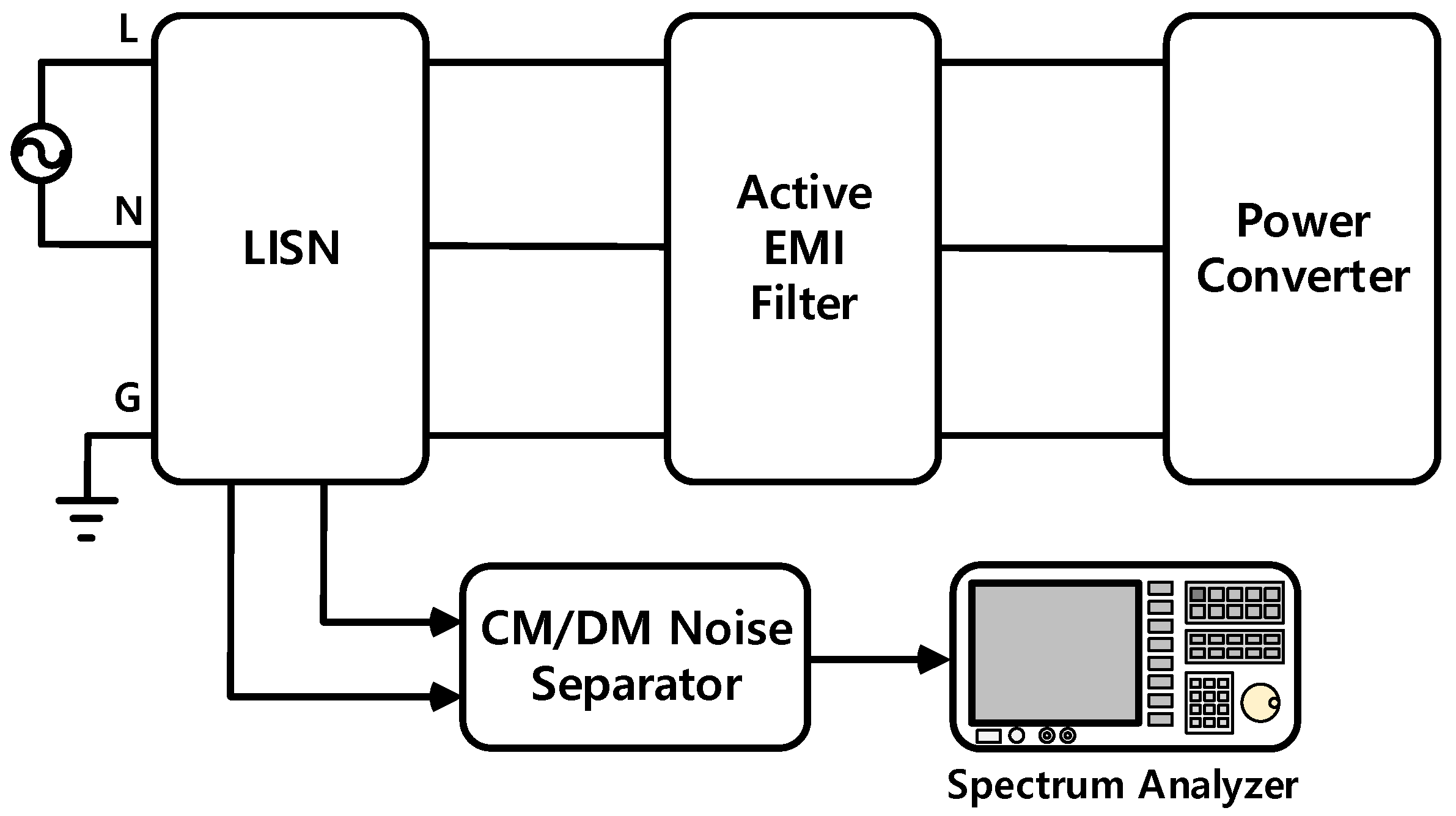
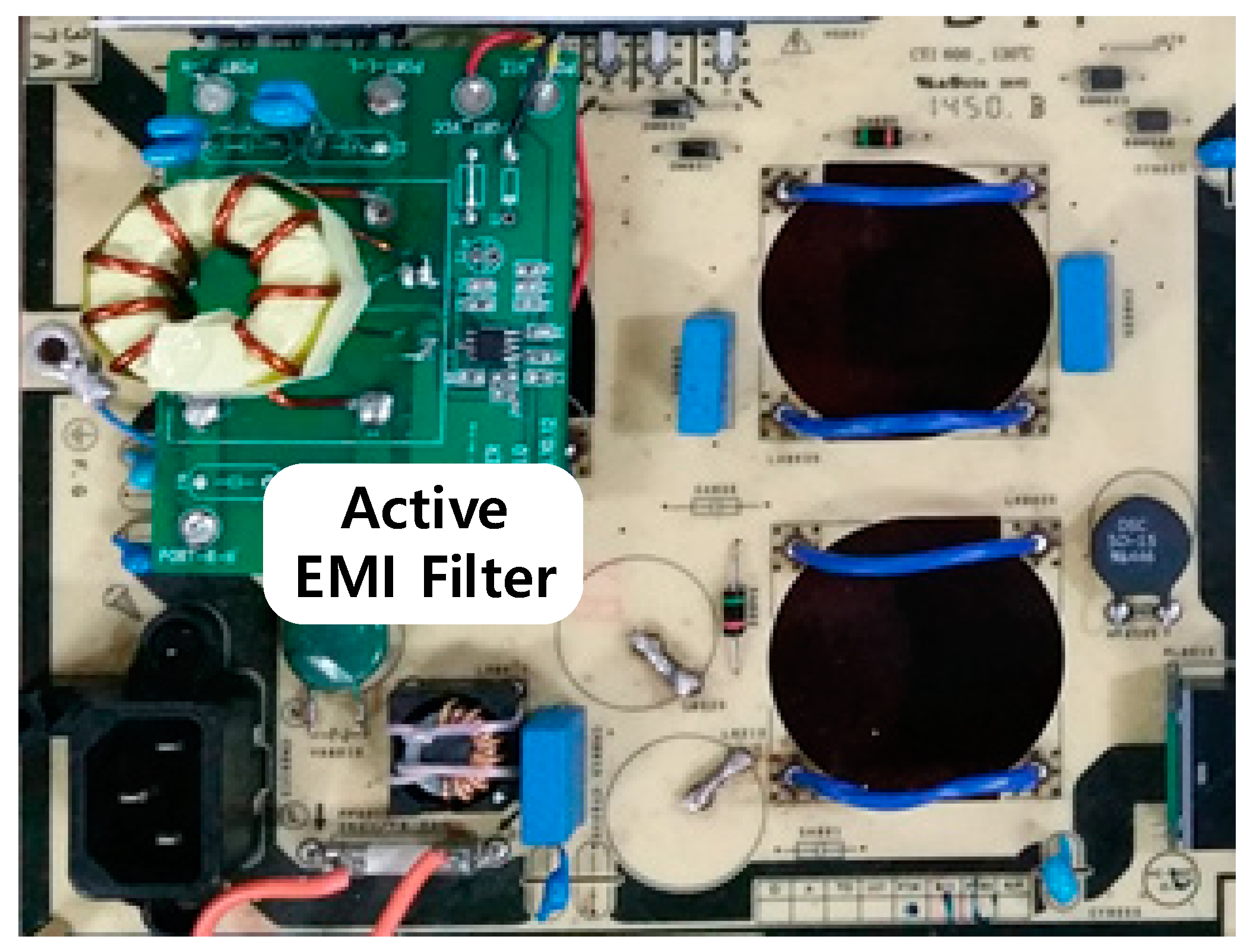
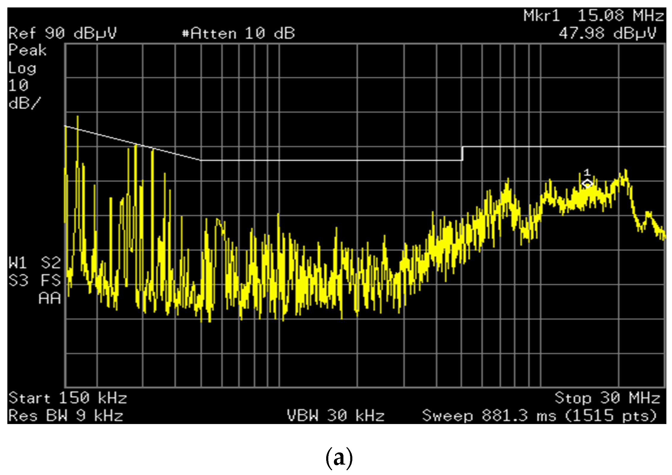
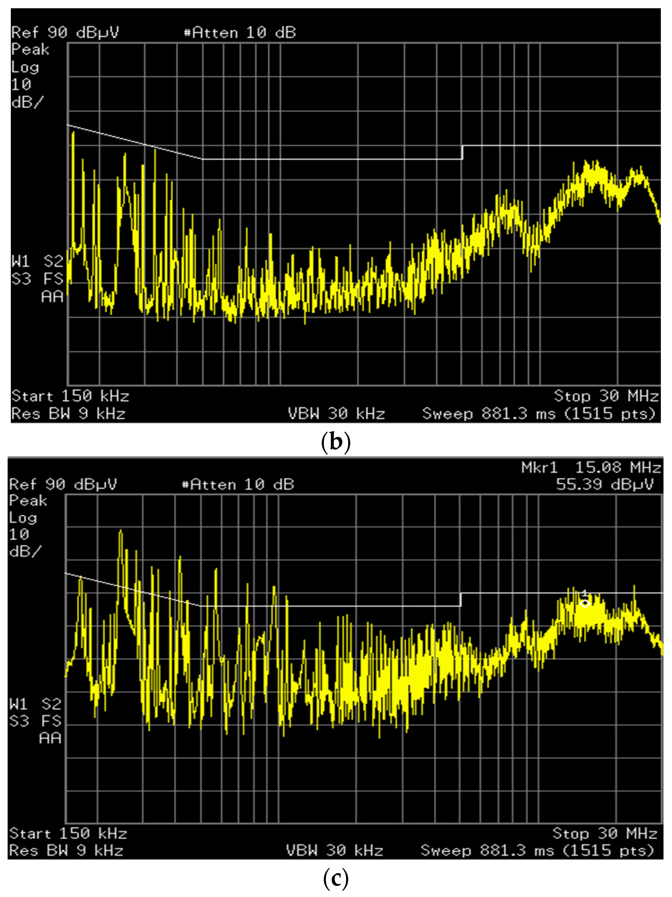
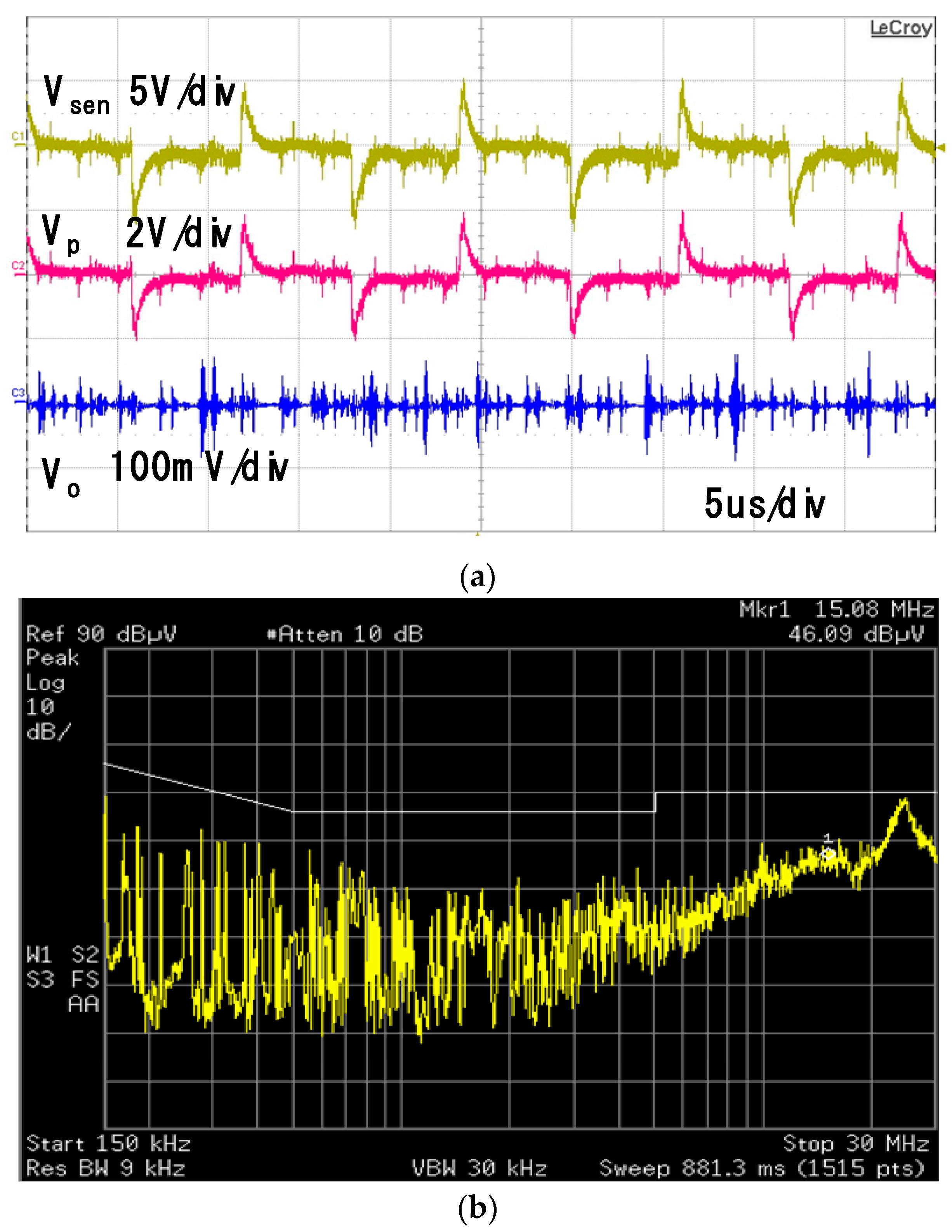
4.1. Experimental Setup

In order to verify theoretic results discussed in the previous sections, the experimental works are performed for the actual feedforward AEF.
Figure 12 shows the experimental setup for testing the EMI reduction performance of the AEF, which consists of the LISN, noise separator, spectrum analyzer, power converter and device under test (AEF). Figure 13 shows the photograph of the power converter with the feedforward AEF. The tested power converter is an AC/DC converter with a power factor correction (PFC) circuit, and its power rating is 500 W, where the AEF with the small CM choke replaces the three-stage passive EMI filter. The parameters of the AEF and test system are the same with those given in Table 1 and Table 2. The input capacitance of the AC/DC converter given in Table 2 is calculated from the measured input impedance using the network analyzer [22,23]. The measured impedance is linearly approximated as the single capacitor as shown in (17) and Table 2. The details for the design of the AEF components are not mentioned because the stability and selection of the AEF gain is the main focus of this paper.

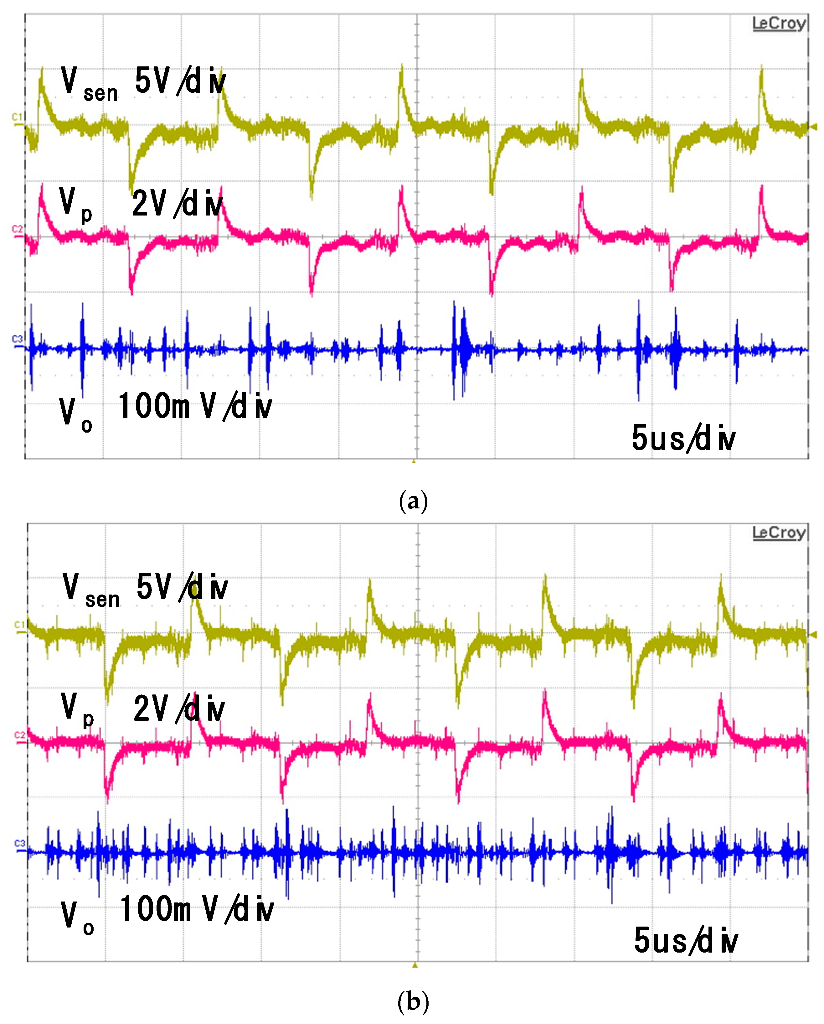
4.2. Experimental Results and Discussions

Figure 14 shows the experimental waveforms for the actual feedforward AEF shown in Figure 13. The sensed noise voltage (Vsen), output voltage of the operational amplifier (Vp) and voltage measured at the LISN terminal (Vo), where the DC gain Kf of the AEF are 0.94, 0.96 and 0.98, respectively. The performance of the noise reduction for the AEF can be determined by the voltage measured at the LISN terminal. As shown in Figure 14a,b, the output voltages of the operational amplifier (Vp) are matched with the sensed noise voltages (Vsen) for the DC gain Kf of 0.94 and 0.96. The high frequency noise only remains in the voltage Vo measured at the LISN terminal. This means that the AEF operation is stable and the noise cancellation is well performed for these gains. It is, however, shown in Figure 14c that the voltage Vp does not follow the sensed voltage (Vsen) for the DC gain Kf of 0.98 and the low frequency noise voltage is shown in the LISN voltage Vo. It is, therefore, noted in this figure that the noise cancellation is not properly performed for this gain. This is because of the unstable operation of the AEF.
Figure 15 shows the frequency response for the ratio of the noise attenuation given in (16) for the three DC gains Kf of 0.94, 0.94 and 0.98, respectively. It is noted in Figure 15c that the noise attenuation of the AEF is not properly done because of the unstable operation of the AEF. Figure 16 shows the EMI spectrums measured at the LISN terminal for the above three DC gains, where the limit line is for the EN55022 regulation. It is shown in Figure 16a,b that the EMI attenuation is well performed in the entire test frequency range of 150 kHz to 30 MHz. In particular, the all frequency components are below the limit line for the DC gain Kf = 0.96. It is known in this result that the EMI reduction performance of the AEF for Kf = 0.96 is better than that for Kf = 0.94. Ideally, the noise voltage decreases to zero as the Kf approaches the unity. However, this is only possible under the stable operation of the AEF. It is shown in Figure 16c that the noise voltage is not properly attenuated for the DC gain Kf = 0.98. As discussed for the results shown in Figure 14 and Figure 15, the AEF is unstable for this gain and the noise attenuation performance is severely degraded for nearly the entire test frequency range of 150 kHz to 30 MHz. It is known, therefore, in Figure 14, Figure 15 and Figure 16 that the DC gain of the AEF should be selected to guarantee the stable operation of the AEF.
As shown in Figure 11, the maximum value of the DC gain depends on the source and load impedances. The higher value of Kf can be applied to the AEF if the CM choke with the lower inductance is used. Figure 17 shows the experimental waveforms for the AEF with the CM choke inductance of LCM = 0.5 mH, where Kf = 0.99. Since the CM choke inductance is reduced to 0.5 mH, the stable range for Kf is extended to the unity as shown in Figure 11, and thus the DC gain of Kf = 0.99 can be applied. It is shown in this experimental result that the noise reduction performance of the AEF is improved because of the higher value of the Kf applied, as shown in the EMI spectrum of the low frequency range of 150 kHz to 500 kHz in Figure 17b. However, the EMI reduction performance of the high frequency range is worse than the that of the AEF with the CM choke inductance of 1 mH. This is because the smaller CM choke is applied and the noise reduction effect by the CM choke thus is degraded. It, therefore, should be required to select the optimum values of both DC gain Kf and CM choke inductance for the best EMI performance. This can be considered as an important issue for further studies.

5. Conclusions

This paper presented the considerations for the gain selection of the feedforward AEF with the VSVC structure. The transfer function employing the source and load impedance was derived, and the stability analysis has been performed for the actual AEF. The gain and phase margins of the loop gain G(s)H(s) were calculated in terms of the DC gain of the AEF for the different source and load impedances. The maximum bound of the DC gain to guarantee the stable operation of the AEF can be obtained from the results of the stability analysis. It is known from the analysis that the noise voltage can be ideally cancelled by applying the unity DC gain of the AEF, but in practice, it causes the unstable operation of the AEF for the certain source and load impedances. Therefore, the source and load impedances are the important factors, and the concept of the symmetry for both aspects should be considered in the selection of the AEF gain.
In order to verify the results of the theoretic analysis, the experimental works are performed for the feedforward AEF used for the actual AC/DC converter with the power rating of 500 W. It is known that the experimental results are well matched with the theoretic analysis. In particualr, the lower source and load impedances provide the possibility of applying the higher value of the AEF gain. However, these conditions do not guarantee the best noise reduction performance because of degrading the noise reduction effect of the CM choke. The optimization between the values of the CM choke inductance and DC gain should be required to achieve the best performance of the AEF.
It is concluded from the theoretic and experimental results of this paper that the important considerations for the gain selection of the AEF can be given as:
  • The stability of the AEF should be checked for the given source and load impedances in selecting the gain of the AEF;
  • The maximum bound of the AEF gain for the given source and load impedances can be obtained from the stability analysis performed in Section 3;
  • Choosing the lower value of the CM choke can extend the maximum bound of the AEF gain guaranteeing the stable operation, but it does not provide the best AEF performance;
  • The optimization between the AEF gain and CM choke is required to achieve the best performance of the AEF.
The results of this paper can be used for the optimum design of the feedforward AEF for the switching power converters.

Author Contributions

Conceptualization, S.-K.C.; methodology, S.-K.C. and B.-G.K.; validation, S.-K.C. and B.-G.K.; formal analysis, S.-K.C. and B.-G.K.; investigation, S.-K.C. and B.-G.K.; data curation, S.-K.C. and B.-G.K.; writing—original draft preparation, S.-K.C.; writing—review and editing, S.-K.C.; supervision, S.-K.C.; project administration, S.-K.C.; funding acquisition, S.-K.C. All authors have read and agreed to the published version of the manuscript.

Funding

This work was supported by the Gyeongsang National University Fund for Professors on Sabbatical Leave, 2019.

Data Availability Statement

Not applicable.

Conflicts of Interest

The authors declare no conflict of interest.

References

  1. Zhang, B.; Wang, S. An overview of wide bandgap power semiconductor device packaging techniques for EMI reduction. In Proceedings of the IEEE Symp. on Electromagnetic Compatibility, Signal Integrity and Power Integrity, Long Beach, CA, USA, 30 July 2018. [Google Scholar]
  2. Han, D.; Li, S.; Wu, Y.; Choi, W.; Sarlioglu, B. Comparative analysis on conducted CM EMI emission of motor drives: WBG versus Si devices. IEEE Trans. Ind. Electron. 2017, 64, 8353–8363. [Google Scholar] [CrossRef]
  3. Shih, F.Y.; Chen, D.Y.; Wu, Y.P.; Chen, Y.T. A procedure for designing EMI filters for AC line applications. IEEE Trans. Power Electron. 1996, 11, 170–181. [Google Scholar] [CrossRef]
  4. Nagle, A.; De Doncker, R.W. Systematic design of EMI-filters for power converters. In Proceedings of the IEEE Industry Applications Conference, Rome, Italy, 8 December 2000. [Google Scholar]
  5. Rossetto, L.; Buso, S.; Spiazzi, G. Conducted EMI issues in a 600-W single phase boost PFC design. IEEE Trans. Ind. Applicat. 2000, 36, 578–585. [Google Scholar] [CrossRef]
  6. Cochrane, D.; Chen, D.; Boroyevich, D. Passive cancellation of common-mode noise in power electronic circuits. IEEE Trans. Power Electron. 2003, 18, 756–763. [Google Scholar]
  7. Ye, S.; Eberle, W.; Liu, Y.-F. A novel EMI filter design method for switching power supplies. IEEE Trans. Power Electron. 2004, 19, 1668–1678. [Google Scholar]
  8. Farkas, T.; Schlecht, M.F. Viability of active EMI filters for utility applications. IEEE Trans. Power Electron. 1994, 9, 328–337. [Google Scholar] [CrossRef]
  9. Son, Y.; Sul, S. A new active common-mode EMI filter for PWM inverter. IEEE Trans. Power Electron. 2003, 18, 1309–1314. [Google Scholar] [CrossRef]
  10. Son, Y.; Sul, S. Generalization of active filters for EMI reduction and harmonics compensation. IEEE Trans. Ind. Appl. 2006, 42, 545–551. [Google Scholar] [CrossRef]
  11. Chen, W.; Yang, X.; Wang, Z. An active EMI filtering technique for improving passive filter low-frequency performance. IEEE Trans. Electromagn. Compat. 2006, 48, 172–177. [Google Scholar] [CrossRef]
  12. Mainali, K.; Oruganti, R. Design of a current-sense voltage-feedback common mode EMI filter for an off-line power converter. In Proceedings of the 2008 IEEE Power Electronics Specialists Conference, Rhodes, Greece, 15 June 2008. [Google Scholar]
  13. Hamza, D.; Jain, P.K. Conducted EMI noise mitigation in DC-DC converters using active filtering method. In Proceedings of the IEEE Power Electronics Specialists Conference, Rhodes, Greece, 15–19 June 2008. [Google Scholar]
  14. Chen, W.; Zhang, W.; Yang, X.; Sheng, Z.; Wang, Z. An experimental study of common- and differential-mode active EMI Filter compensation characteristics. IEEE Trans. Electromagn. Compat 2009, 51, 683–691. [Google Scholar] [CrossRef]
  15. Heldwein, M.L.; Ertl, H.; Biela, J.; Kolar, J.W. Implementation of a transformerless common-mode active filter for offline converter systems. IEEE Trans. Ind. Electron. 2020, 57, 1772–1786. [Google Scholar] [CrossRef]
  16. Hamza, D.; Sawan, M.; Jain, P.K. Suppression of common-mode input electromagnetic interference noise in DC–DC converters using the active filtering method. IET Power Electron. 2011, 4, 776–784. [Google Scholar] [CrossRef]
  17. Rong, Z.; Panlong, F.; Wei, D.; Rui, X. Design of active EMI filter based on virtual impedance transform method. In Proceedings of the 2nd International Symposium on Instrumentation and Measurement, Sensor Network and Automation (IMSNA), Toronto, ON, Canada, 23–24 December 2013; pp. 871–874. [Google Scholar]
  18. Ali, M.; Labour’e, E.; Costa, F. Integrated active filter for differential-mode noise suppression. IEEE Trans. Power Electron. 2014, 29, 1053–1057. [Google Scholar] [CrossRef]
  19. Lee, K.H.; Kang, B.G.; Choi, Y.H.; Chung, S.K. Design and implementation of active EMI filter for common-mode noise reduction. J. Power Electron. 2016, 16, 1236–1243. [Google Scholar] [CrossRef]
  20. Dai, L.; Chen, W.; Yang, Y.; Wang, R.; Yang, X. Design of active EMI filters with the integrated passive component. In Proceedings of the IEEE Applied Power Electronics Conference and Exposition (APEC), Anaheim, CA, USA, 17–21 March 2019. [Google Scholar]
  21. Zhang, Z.; Bazzi, A.M. Modeling, design, and implementation of a novel transformer-less feedforward-controlled active EMI filter for AC-DC power converters. In Proceedings of the IEEE Energy Conversion Congress and Exposition (ECCE), Detroit, MI, USA, 11–15 October 2020. [Google Scholar]
  22. Zhang, D.; Chen, D.Y.; Nave, M.J.; Sable, D. Measurement of noise source impedance of off-line converters. IEEE Trans. Power Electron. 2000, 15, 820–825. [Google Scholar] [CrossRef]
  23. See, K.T.; Deng, J. Measurement of noise source impedance of SMPS using a two probes approach. IEEE Trans. Power Electron. 2004, 19, 862–868. [Google Scholar] [CrossRef]
Figure 1. Common mode active EMI filter with VSVC-type feedforward structure [19].
Symmetry 14 01826 g001
Figure 2. Equivalent circuits of feedback and feedforward AEFs in CM [19]: (a) feedback AEF; (b) feedforward AEF.
Symmetry 14 01826 g002
Figure 3. Detailed CM equivalent circuit of VSVC-type feedforward AEF.
Symmetry 14 01826 g003
Figure 4. Simplified equivalent circuit of cancellation transformer.
Symmetry 14 01826 g004
Figure 5. Bode plot of AEF gain A(s) for Kf = 1.
Symmetry 14 01826 g005
Figure 6. Bode plot of cancelled output 1−A(s) for Kf = 1.
Symmetry 14 01826 g006
Figure 7. Bode plot of loop gain G(s)H(s): (a) Kf = 0.94; (b) Kf = 0.97; (c) Kf = 1.
Symmetry 14 01826 g007
Figure 8. Bode plot of loop gain G(s)H(s) for different input impedances (Kf = 0.97): (a) Cin = 45 nF; (b) Cin = 15 nF.
Symmetry 14 01826 g008
Figure 9. Gain and phase margins of AEF for various Kf and input impedances.
Symmetry 14 01826 g009
Figure 10. Bode plot of loop gain G(s)H(s) for different load impedances (Kf = 0.97): (a) LCM = 0.5 mH; (b) LCM = 1.5 mH.
Symmetry 14 01826 g010
Figure 11. Gain and phase margins of AEF for various Kf and CM choke inductances.
Symmetry 14 01826 g011
Figure 12. Experimental setup for testing EMI reduction performance of AEF.
Symmetry 14 01826 g012
Figure 13. Experimental power converter with feedforward AEF.
Symmetry 14 01826 g013
Figure 14. Experimental waveforms for the sensed noise voltage (Vsen), output voltage of the operational amplifier (Vp) and voltage of the LISN terminal (Vo): (a) Kf = 0.94; (b) Kf = 0.96; (c) Kf = 0.98.
Symmetry 14 01826 g014aSymmetry 14 01826 g014b
Figure 15. Frequency response for ratio of noise attenuation: (a) Kf = 0.94; (b) Kf = 0.96; (c) Kf = 0.98.
Symmetry 14 01826 g015aSymmetry 14 01826 g015b
Figure 16. Experimental waveforms for the EMI spectrum measured at the LISN terminal: (a) Kf = 0.94; (b) Kf = 0.96; (c) Kf = 0.98.
Symmetry 14 01826 g016aSymmetry 14 01826 g016b
Figure 17. Experimental waveforms for the CM choke inductance = 0.5 mH and Kf = 0.99: (a) Sensed noise voltage (Vsen), output voltage of the operational amplifier (Vp) and voltage of the LISN terminal (Vo); (b) EMI spectrum.
Symmetry 14 01826 g017
Table 1. Parameters of AEF components.
ItemValue
Cs20 nF
R110 kΩ
Llk2.8 uH
Cp80 pF
LM220 uH
n2
Table 2. Parameters of source and load impedances.
ItemValue
Cin31.1 nF
CCM10 pF
LCM1 mH
RL25 Ω
CL0.2 uF
Publisher’s Note: MDPI stays neutral with regard to jurisdictional claims in published maps and institutional affiliations.

