

Instruction-Fetching Attack and Practice in Collision Fault Attack on AES


Abstract
1. Introduction
2. Related Works
- Instruction-executing fault: This kind of fault is induced by disturbing the normal execution of instructions, e.g., making the executed operation not complete normally by underpowering or providing a clock glitch, which is widely used in actual attacks. The core idea of this technology is that reducing the supply voltage of the device can temporarily extend the key-path of the circuit, or the rising edge of the clock glitch will cause an error data to be stored in the Flip-Flop in advance [23,24].
- Instruction-fetching fault: This article focuses only on this type of fault. The core idea is to modify the program data to be stored in the instruction register by introducing interference to the on-chip Flash during instruction-fetching, and then the microcontroller executes a wrong instruction. There is no uniform name for this type of attack. Some works only focused on Instruction Skip [25,26], and some other works summarized it as Instruction Replacement [12] or Instruction Corruption [13]. To describe this concept more accurately, the term instruction-fetching fault is applied in this paper.
3. Attack Model
3.1. The Advanced Encryption Standard
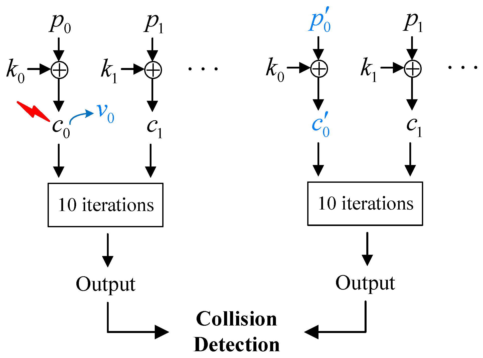
3.2. CFA Model Based on Instruction Skip

 |
3.2.1. Skiping the LD Instruction
| Algorithm 1: An algorithm of key calculation for LD skipping model. |
 |
3.2.2. Skippping EOR or ST Instruction
| Algorithm 2: An algorithm of key calculation for EOR or ST skipping model. |
 |
3.3. Summary
4. Experimental Setting
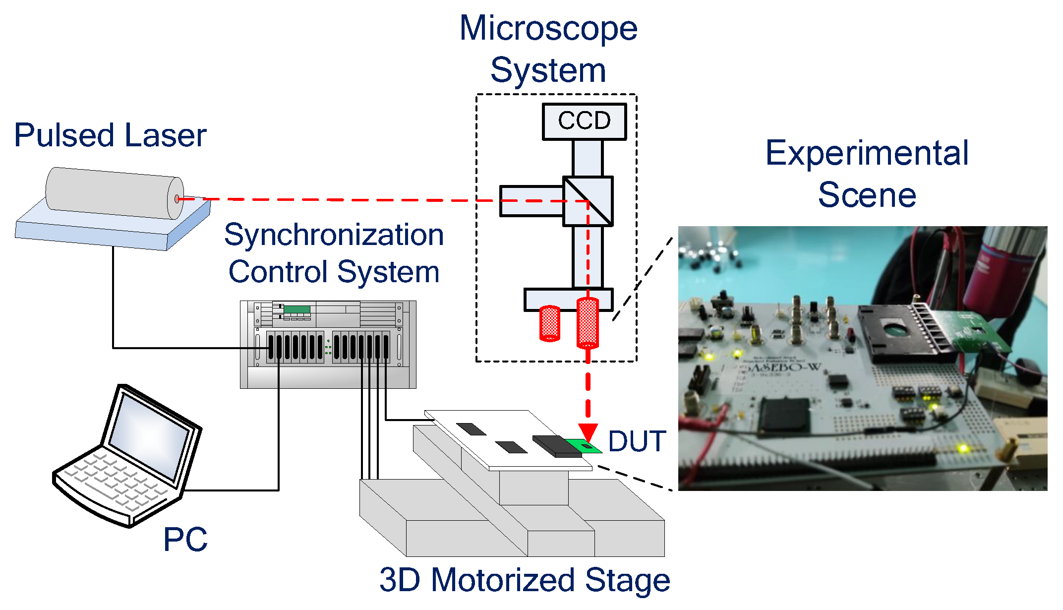
4.1. The Pulsed Laser Fault Injection Platform
- A pulsed laser and optical path system
- A 3D mobile station
- Synchronous control system (responsible for timing control of different elements)
- An oscilloscope
- A control PC
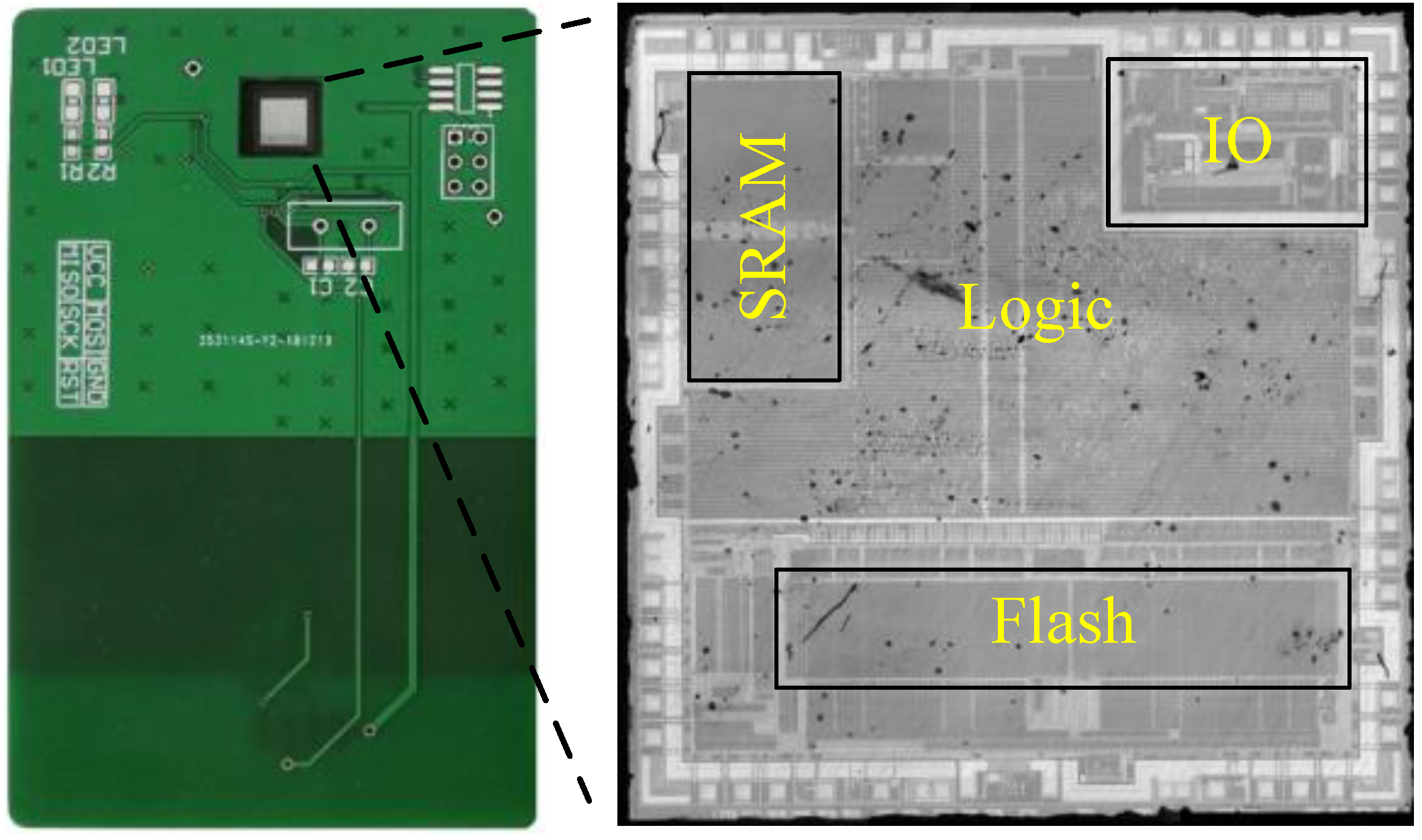
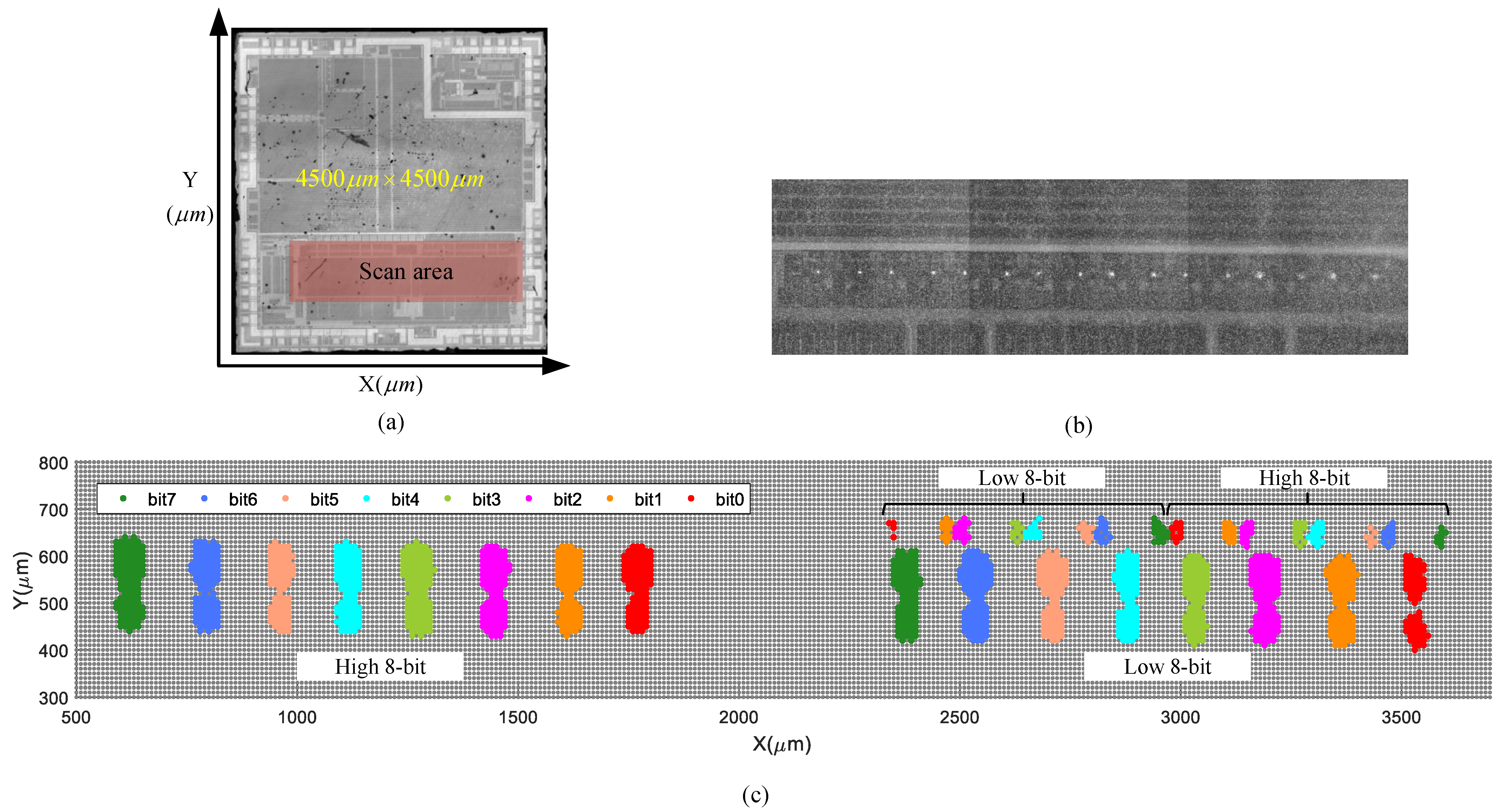
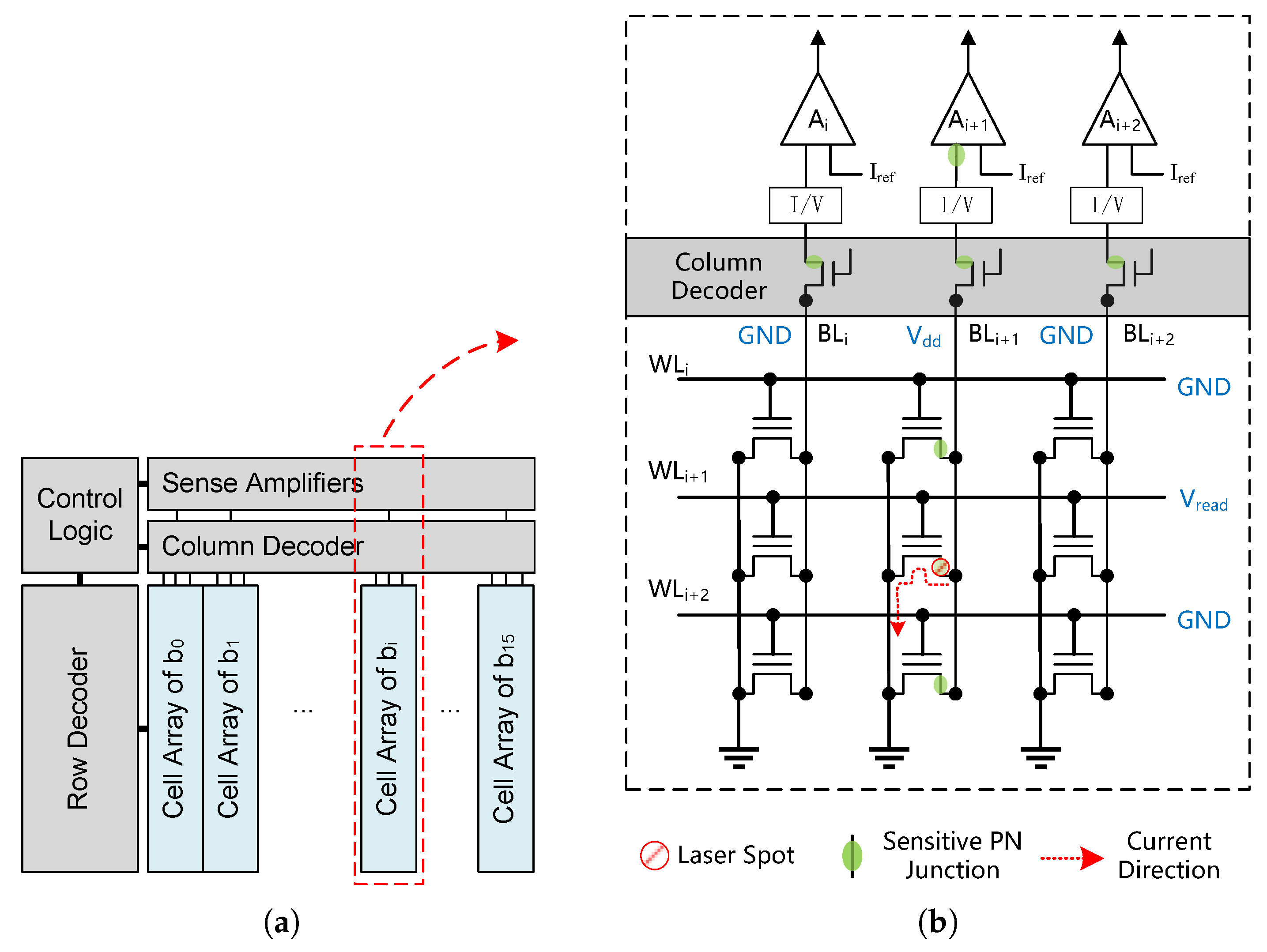
4.2. Test Chip
5. Experimental Result
5.1. Laser-Induced Flash-Data-Accessing Error
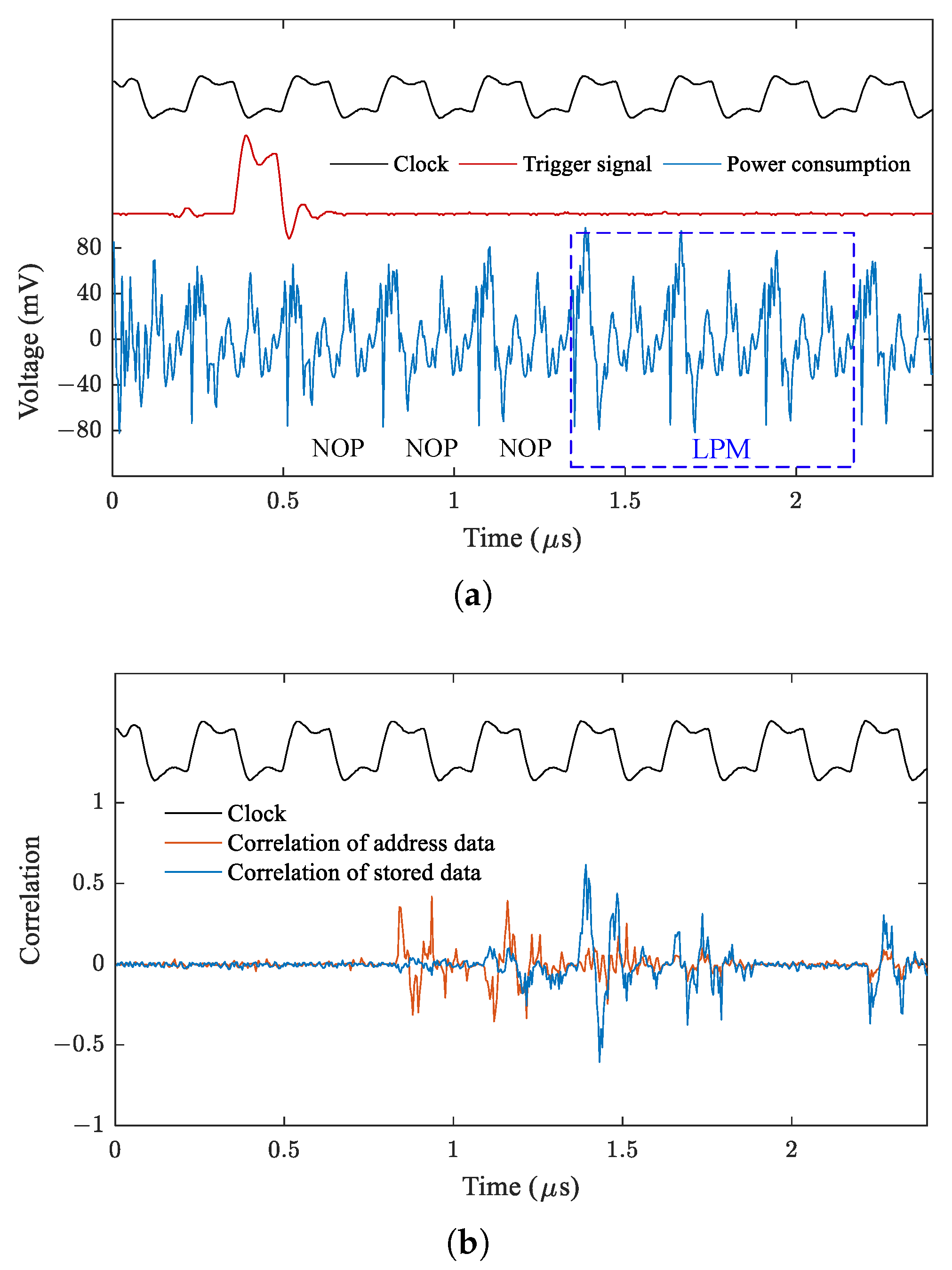
5.1.1. Target the LPM instruction
 |
5.1.2. Sensitive Areas of Laser Injection
- Sensitive areas of laser injection of the same bit of all words are distributed in clusters in the same area.
- There are 16 highlighted areas in the upper right corner of the Flash, which also correspond to 16-bit sensitive areas, respectively. The attack effect against these areas is consistent with the above. We further track the photon radiation of the Flash region and find 16 conspicuous photon leakage points in the upper right corner, as shown in Figure 6b, which indicates that there are frequent transistor switching operations in this area. These areas may indicate the control register location in the Flash read–write control circuit.
- These faults are not permanent. These faults only correspond to the error of read-out data and do not change data stored in Flash cells.
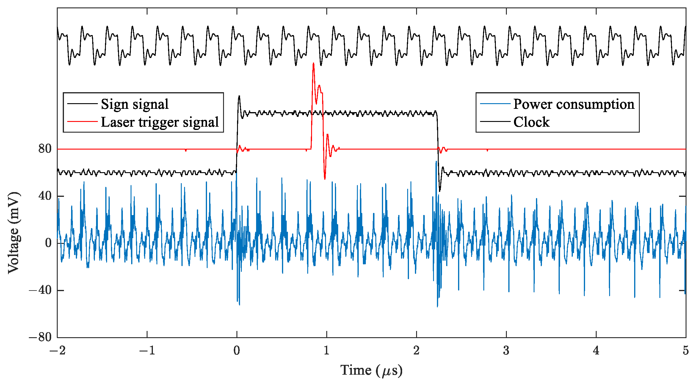
- There is a large effective time window for triggering the laser, which is about 840ns. This may be due to the long duration of Flash data access.
5.2. Attacks on LD, EOR and ST Instructions
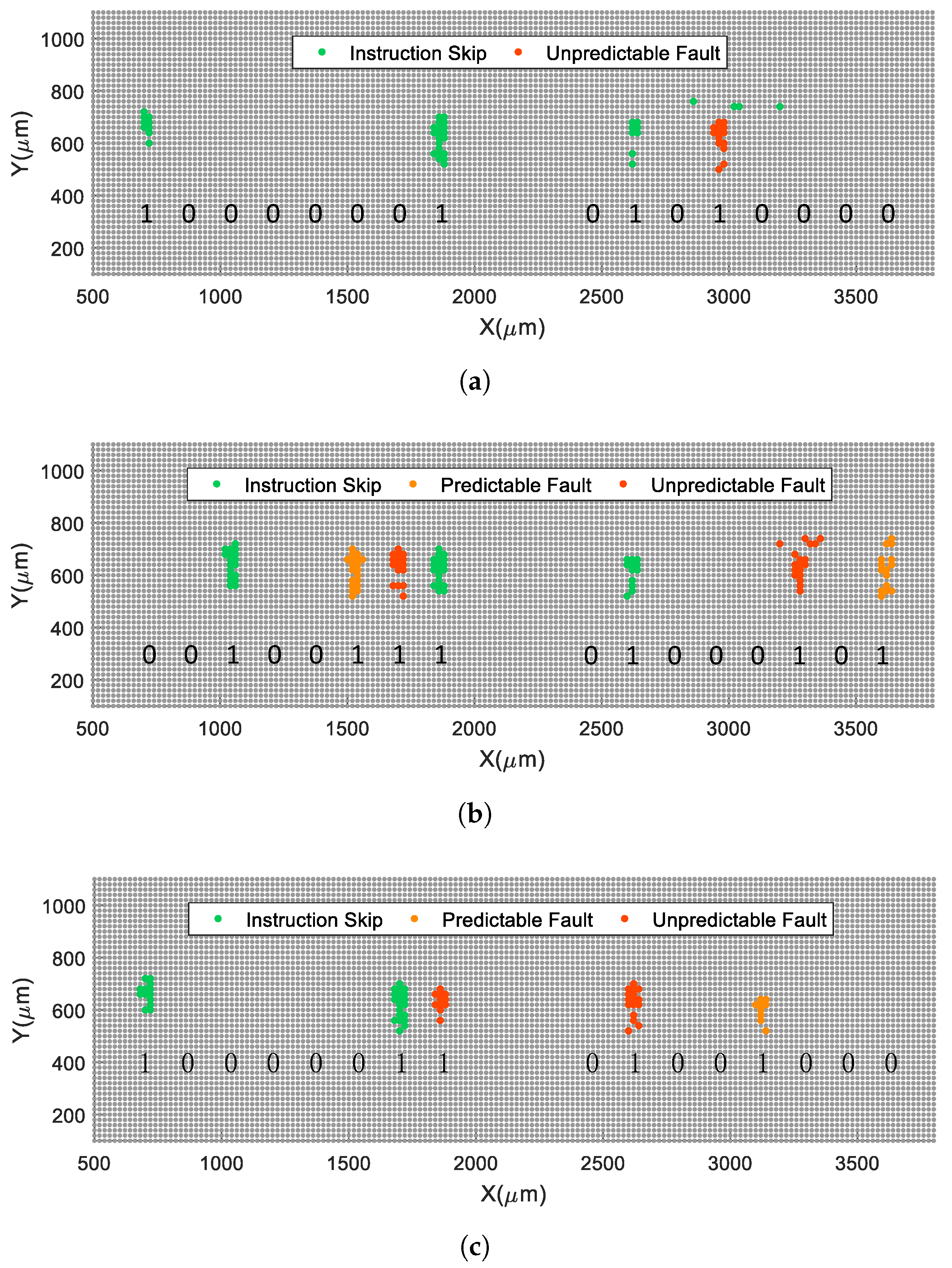
5.2.1. Instruction Skip
5.2.2. Unpredictable Fault
5.2.3. Predictable Fault
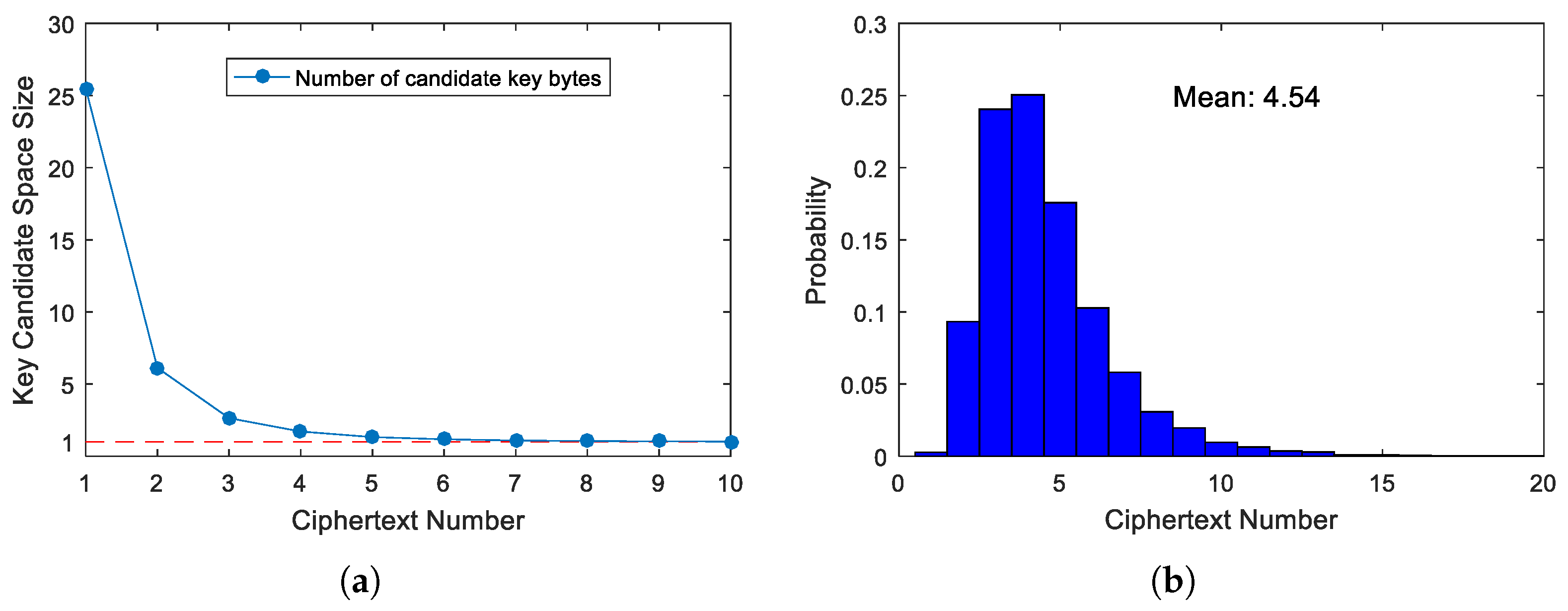
5.3. Key Recovery for the Predictable Fault
5.3.1. EOR R20, R21 → AND R20, R21
| Algorithm 3: Key recovery algorithm for the fault instruction AND R20, R21. |
 |
5.3.2. EOR R20, R21 → EOR R20, R20
5.3.3. ST Y, R20 → ST Z, R20
6. Discussion on the Fault Model of Flash
7. Conclusions
Author Contributions
Funding
Data Availability Statement
Conflicts of Interest
References
- Kocher, P.C. Timing attacks on implementations of Diffie-Hellman, RSA, DSS, and other systems. In Proceedings of the Annual International Cryptology Conference, Santa Barbara, CA, USA, 18–22 August 1996; Springer: Berlin/Heidelberg, Germany, 1996; pp. 104–113. [Google Scholar]
- Gandolfi, K.; Mourtel, C.; Olivier, F. Electromagnetic analysis: Concrete results. In Proceedings of the International Workshop on Cryptographic Hardware and Embedded Systems, Paris, France, 14–16 May 2001; Springer: Berlin/Heidelberg, Germany, 2001; pp. 251–261. [Google Scholar]
- Kocher, P.; Jaffe, J.; Jun, B. Differential power analysis. In Proceedings of the Annual International Cryptology Conference, Santa Barbara, CA, USA, 15–19 August 1999; Springer: Berlin/Heidelberg, Germany, 1999; pp. 388–397. [Google Scholar]
- Boneh, D.; DeMillo, R.A.; Lipton, R.J. On the importance of checking cryptographic protocols for faults. In Proceedings of the International Conference on the Theory and Applications of Cryptographic Techniques, Konstanz, Germany, 11–15 May 1997; Springer: Berlin/Heidelberg, Germany, 1997; pp. 37–51. [Google Scholar]
- Schmidt, J.M.; Herbst, C. A practical fault attack on square and multiply. In Proceedings of the 2008 5th Workshop on Fault Diagnosis and Tolerance in Cryptography, Washington, DC, USA, 10–10 August 2008; pp. 53–58. [Google Scholar]
- Choukri, H.; Tunstall, M. Round reduction using faults. FDTC 2005, 5, 13–24. [Google Scholar]
- Schmidt, J.M.; Hutter, M. Optical and em Fault-Attacks on Crt-Based Rsa: Concrete Results. In Proceedings of the Austrochip 2007, 15th Austrian Workhop on Microelectronics, Graz, Austria, 11 October 2007; pp. 61–67. [Google Scholar]
- Skorobogatov, S.P.; Anderson, R.J. Optical fault induction attacks. In Proceedings of the International Workshop on Cryptographic Hardware and Embedded Systems, Redwood Shores, CA, USA, 13–15 August 2002; Springer: Berlin/Heidelberg, Germany, 2002; pp. 2–12. [Google Scholar]
- Balasch, J.; Gierlichs, B.; Verbauwhede, I. An In-depth and Black-box Characterization of the Effects of Clock Glitches on 8-bit MCUs. In Proceedings of the 2011 Workshop on Fault Diagnosis and Tolerance in Cryptography, Nara, Japan, 28 September 2011; pp. 105–114. [Google Scholar]
- Moro, N.; Dehbaoui, A.; Heydemann, K.; Robisson, B.; Encrenaz, E. Electromagnetic fault injection: Towards a fault model on a 32-bit microcontroller. In Proceedings of the 2013 Workshop on Fault Diagnosis and Tolerance in Cryptography, Los Alamitos, CA, USA, 20 August 2013; pp. 77–88. [Google Scholar]
- Trabelsi, O.; Sauvage, L.; Danger, J.L. Characterization of electromagnetic fault injection on a 32-bit microcontroller instruction buffer. In Proceedings of the 2020 Asian Hardware Oriented Security and Trust Symposium (AsianHOST), Kolkata, India, 15–17 December 2020; pp. 1–6. [Google Scholar]
- Sakamoto, J.; Fujimoto, D.; Matsumoto, T. Laser-induced controllable instruction replacement fault attack. IEICE Trans. Fundam. Electron. Commun. Comput. Sci. 2020, 103, 11–20. [Google Scholar] [CrossRef]
- Colombier, B.; Menu, A.; Dutertre, J.M.; Moëllic, P.A.; Rigaud, J.B.; Danger, J.L. Laser-induced single-bit faults in flash memory: Instructions corruption on a 32-bit microcontroller. In Proceedings of the 2019 IEEE International Symposium on Hardware Oriented Security and Trust (HOST), McLean, VA, USA, 5–10 May 2019; pp. 1–10. [Google Scholar]
- Khuat, V.; Danger, J.L.; Dutertre, J.M. Laser Fault Injection in a 32-bit Microcontroller: From the Flash Interface to the Execution Pipeline. In Proceedings of the 2021 Workshop on Fault Detection and Tolerance in Cryptography (FDTC), Milan, Italy, 17 September 2021; pp. 74–85. [Google Scholar]
- Menu, A.; Dutertre, J.M.; Rigaud, J.B.; Colombier, B.; Moellic, P.A.; Danger, J.L. Single-bit laser fault model in NOR flash memories: Analysis and exploitation. In Proceedings of the 2020 Workshop on Fault Detection and Tolerance in Cryptography (FDTC), Milan, Italy, 13 September 2020; pp. 41–48. [Google Scholar]
- Biham, E.; Shamir, A. Differential fault analysis of secret key cryptosystems. In Proceedings of the Annual International Cryptology Conference, Santa Barbara, CA, USA, 17–21 August 1997; Springer: Berlin/Heidelberg, Germany, 1997; pp. 513–525. [Google Scholar]
- Kim, C.H.; Quisquater, J.J. New differential fault analysis on AES key schedule: Two faults are enough. In Proceedings of the International Conference on Smart Card Research and Advanced Applications, London, UK, 8–11 September 2008; Springer: Berlin/Heidelberg, Germany, 2008; pp. 48–60. [Google Scholar]
- Blömer, J.; Seifert, J.P. Fault based cryptanalysis of the advanced encryption standard (AES). In Proceedings of the International Conference on Financial Cryptography, Guadeloupe, French West Indies, 27–30 January 2003; Springer: Berlin/Heidelberg, Germany, 2003; pp. 162–181. [Google Scholar]
- Zhang, F.; Zhang, Y.; Jiang, H.; Zhu, X.; Bhasin, S.; Zhao, X.; Liu, Z.; Gu, D.; Ren, K. Persistent fault attack in practice. IACR Trans. Cryptogr. Hardw. Embed. Syst. 2020, 2020, 172–195. [Google Scholar] [CrossRef]
- Hemme, L. A differential fault attack against early rounds of (triple-) DES. In Proceedings of the International Workshop on Cryptographic Hardware and Embedded Systems, Cambridge, MA, USA, 11–13 August 2004; Springer: Berlin/Heidelberg, Germany, 2004; pp. 254–267. [Google Scholar]
- Blömer, J.; Krummel, V. Fault based collision attacks on AES. In Proceedings of the International Workshop on Fault Diagnosis and Tolerance in Cryptography, Yokohama, Japan, 10 October 2006; Springer: Berlin/Heidelberg, Germany, 2006; pp. 106–120. [Google Scholar]
- Tunstall, M.; Mukhopadhyay, D.; Ali, S. Differential fault analysis of the advanced encryption standard using a single fault. In Proceedings of the IFIP International Workshop on Information Security Theory and Practices, Heraklion, Crete, Greece, 1–3 June 2011; Springer: Berlin/Heidelberg, Germany, 2011; pp. 224–233. [Google Scholar]
- Selmane, N.; Guilley, S.; Danger, J.L. Practical setup time violation attacks on AES. In Proceedings of the 2008 Seventh European Dependable Computing Conference, Kaunas, Lithuania, 7–9 May 2008; pp. 91–96. [Google Scholar]
- Bhasin, S.; Selmane, N.; Guilley, S.; Danger, J.L. Security evaluation of different AES implementations against practical setup time violation attacks in FPGAs. In Proceedings of the 2009 IEEE International Workshop on Hardware-Oriented Security and Trust, San Francisco, CA, USA, 27 July 2009; pp. 15–21. [Google Scholar]
- Yuce, B.; Ghalaty, N.F.; Santapuri, H.; Deshpande, C.; Patrick, C.; Schaumont, P. Software fault resistance is futile: Effective single-glitch attacks. In Proceedings of the 2016 Workshop on Fault Diagnosis and Tolerance in Cryptography (FDTC); IEEE: Toulouse, France, 2016; pp. 47–58. [Google Scholar]
- Dutertre, J.M.; Riom, T.; Potin, O.; Rigaud, J.B. Experimental analysis of the laser-induced instruction skip fault model. In Proceedings of the Nordic Conference on Secure IT Systems, Santa Barbara, CA, USA, 16 August 2016; Springer: Berlin/Heidelberg, Germany, 2019; pp. 221–237. [Google Scholar]
- Elmohr, M.A.; Liao, H.; Gebotys, C.H. EM fault injection on ARM and RISC-V. In Proceedings of the 2020 21st International Symposium on Quality Electronic Design (ISQED), Santa Clara, CA, USA, 25–26 March 2020; pp. 206–212. [Google Scholar]
- Kumar, D.S.; Beckers, A.; Balasch, J.; Gierlichs, B.; Verbauwhede, I. An in-depth and black-box characterization of the effects of laser pulses on atmega328p. In Proceedings of the International Conference on Smart Card Research and Advanced Applications, Montpellier, France, 12–14 November 2018; Springer: Berlin/Heidelberg, Germany, 2018; pp. 156–170. [Google Scholar]
- Khuat, V.; Dutertre, J.M.; Danger, J.L. Analysis of a laser-induced instructions replay fault model in a 32-bit microcontroller. In Proceedings of the 2021 24th Euromicro Conference on Digital System Design (DSD), Palermo, Italy, 1–3 September 2021; pp. 363–370. [Google Scholar]
- Vasselle, A.; Thiebeauld, H.; Maouhoub, Q.; Morisset, A.; Ermeneux, S. Laser-induced fault injection on smartphone bypassing the secure boot. In Proceedings of the 2017 Workshop on Fault Diagnosis and Tolerance in Cryptography (FDTC), Taipei, Taiwan, 25 September 2017; pp. 41–48. [Google Scholar]
- Gaine, C.; Aboulkassimi, D.; Pontié, S.; Nikolovski, J.P.; Dutertre, J.M. Electromagnetic fault injection as a new forensic approach for SoCs. In Proceedings of the 2020 IEEE International Workshop on Information Forensics and Security (WIFS), New York, NY, USA, 6–11 December 2020; pp. 1–6. [Google Scholar]
- Daemen, J.; Rijmen, V. Reijndael: The Advanced Encryption Standard. Dr. Dobb’s J. Softw. Tools Prof. Program. 2001, 26, 137–139. [Google Scholar]
- Roscian, C.; Sarafianos, A.; Dutertre, J.M.; Tria, A. Fault model analysis of laser-induced faults in sram memory cells. In Proceedings of the 2013 Workshop on Fault Diagnosis and Tolerance in Cryptography, Los Alamitos, CA, USA, 20 August 2013; pp. 89–98. [Google Scholar]
- Richter, D. Fundamentals of non-volatile memories. In Flash Memories; Springer: Berlin/Heidelberg, Germany, 2014; pp. 5–110. [Google Scholar]
- Amiel, F.; Villegas, K.; Feix, B.; Marcel, L. Passive and active combined attacks: Combining fault attacks and side channel analysis. In Proceedings of the Workshop on Fault Diagnosis and Tolerance in Cryptography (FDTC 2007), Vienna, Austria, 10 September 2007; pp. 92–102. [Google Scholar]


| Methods | Temporal & Spatial Accuracy | Performance of Instruction Tampering |
|---|---|---|
| Voltage glitch | High & Low | Not controllable [6] |
| Clock glitch | High & Low | Not controllable [9] |
| Electromagnetic pulse | High & Ordinary | Ordinary [10,11] |
| Laser injection | High & High | Controllable [12], ours |
| Index of the Key Byte | Register | Instruction Skip | LD | EOR | ST |
|---|---|---|---|---|---|
| 1st | R20 | Before After | |||
| R21 | Before After | ||||
| 2nd | R20 | Before After | |||
| R21 | Before After | ||||
| . . . | . . . | . . . | . . . | . . . | . . . |
| 15th | R20 | Before After | |||
| R21 | Before After |
| Format | Opcodes |
|---|---|
| LPM | 1001 0101 1100 1000 |
| LPM Rd *, Z | 1001 000d dddd 0100 |
| LPM Rd, Z+ | 1001 000d dddd 0101 |
| Modified Bit-1 Position | Opcodes | Operation Instruction | Effect |
|---|---|---|---|
| None | 1000 0001 0101 0000 | LD R21, Z | Normal |
| 1st | 0000 0001 0101 0000 | MOVW R10, R0 | Skipping |
| 2nd | 1000 0000 0101 0000 | LD R5, Z | Skipping |
| 3rd | 1000 0001 0001 0000 | LD R17, Z | Skipping |
| 4th | 1000 0001 0100 0000 | LD R20, Z | Unpredictable |
| Modified Bit-1 Position | Opcodes | Operation Instruction | Effect |
|---|---|---|---|
| None | 0010 0111 0100 0101 | EOR R20, R21 | Normal |
| 1st | 0000 0111 0100 0101 | CPC R20, R21 | Skipping |
| 2nd | 0010 0011 0100 0101 | AND R20, R21 | Predictable |
| 3rd | 0010 0101 0100 0101 | EOR R20, R5 | Unpredictable |
| 4th | 0010 0110 0100 0101 | EOR R4, R21 | Skipping |
| 5th | 0010 0111 0000 0101 | EOR R16, R21 | Skipping |
| 6th | 0010 0111 0100 0001 | EOR R20, R17 | Unpredictable |
| 7th | 0010 0111 0100 0100 | EOR R20, R20 | Predictable |
| Modified Bit-1 Position | Opcodes | Operation Instruction | Effect |
|---|---|---|---|
| None | 1000 0011 0100 1000 | ST Y, R20 | Normal |
| 1st | 0000 0011 0100 1000 | FMUL R20, R16 | Skipping |
| 2nd | 1000 0001 0100 1000 | LD R20, Y | Skipping |
| 3rd | 1000 0010 0100 1000 | ST Y, R4 | Unpredictable |
| 4th | 1000 0011 0000 1000 | ST Y, R16 | Unpredictable |
| 5th | 1000 0011 0100 0000 | ST Z, R20 | Predictable |
Publisher’s Note: MDPI stays neutral with regard to jurisdictional claims in published maps and institutional affiliations. |
© 2022 by the authors. Licensee MDPI, Basel, Switzerland. This article is an open access article distributed under the terms and conditions of the Creative Commons Attribution (CC BY) license (https://creativecommons.org/licenses/by/4.0/).
Share and Cite
Jiang, H.; Zhu, X.; Han, J. Instruction-Fetching Attack and Practice in Collision Fault Attack on AES. Symmetry 2022, 14, 2201. https://doi.org/10.3390/sym14102201
Jiang H, Zhu X, Han J. Instruction-Fetching Attack and Practice in Collision Fault Attack on AES. Symmetry. 2022; 14(10):2201. https://doi.org/10.3390/sym14102201
Chicago/Turabian StyleJiang, Huilong, Xiang Zhu, and Jianwei Han. 2022. "Instruction-Fetching Attack and Practice in Collision Fault Attack on AES" Symmetry 14, no. 10: 2201. https://doi.org/10.3390/sym14102201
APA StyleJiang, H., Zhu, X., & Han, J. (2022). Instruction-Fetching Attack and Practice in Collision Fault Attack on AES. Symmetry, 14(10), 2201. https://doi.org/10.3390/sym14102201