Article

Design and Robustness Evaluation of Valley Topological Elastic Wave Propagation in a Thin Plate with Phononic Structure

Department of Electrical and Electronic Engineering, Okayama University, Okayama 700-8530, Japan
*
Author to whom correspondence should be addressed.
Symmetry 2022, 14(10), 2133; https://doi.org/10.3390/sym14102133
Submission received: 22 September 2022 / Revised: 7 October 2022 / Accepted: 8 October 2022 / Published: 13 October 2022
(This article belongs to the Section Physics)

Abstract

:
Based on the concept of band topology in phonon dispersion, we designed a topological phononic crystal in a thin plate for developing an efficient elastic waveguide. Despite that various topological phononic structures have been actively proposed, a quantitative design strategy of the phononic band and its robustness assessment in an elastic regime are still missing, hampering the realization of topological acoustic devices. We adopted a snowflake-like structure for the crystal unit cell and determined the optimal structure that exhibited the topological phase transition of the planar phononic crystal by changing the unit cell structure. The bandgap width could be adjusted by varying the length of the snow-side branch, and a topological phase transition occurred in the unit cell structure with threefold rotational symmetry. Elastic waveguides based on edge modes appearing at interfaces between crystals with different band topologies were designed, and their transmission efficiencies were evaluated numerically and experimentally. The results demonstrate the robustness of the elastic wave propagation in thin plates. Moreover, we experimentally estimated the backscattering length, which measures the robustness of the topologically protected propagating states against structural inhomogeneities. The results quantitatively indicated that degradation of the immunization against the backscattering occurs predominantly at the corners in the waveguides, indicating that the edge mode observed is a relatively weak topological state.

1. Introduction

Acoustic waveguides based on phononic crystals [1,2,3,4,5,6,7,8,9,10] have been attracting increasing attention for controlling wave transmission along designed paths at desired operating frequencies [11,12,13,14] using a band-engineering scheme similar to the electronic structure design in semiconductors. However, the practical application of acoustic waveguides using phononic crystals has been hindered by inevitable transmission loss owing to the scattering of sound waves at defects and bending in the waveguide [13,14]. In this study, we adopt the concept of a topological insulator (TI) for a phononic band design. In recent years, considerable attention has been paid to topological insulators, materials that are insulators inside objects but exhibit metallic properties at surfaces [15,16]. The electronic energy dispersion in the material can be devised to design highly efficient conduction at the surface/interface based on bulk-edge correspondence [17]. A TI undergoes a topological transition in the electronic wavefunction via a continuous change in the structure/phase. Such topological phase transitions can also occur in classical wave propagation modes in periodic structures [18]. Consequently, the topologically protected edge state that appears at the interface enables highly robust sound wave control against defects and bending in the waveguide [18,19,20,21,22,23,24,25,26,27].
We have previously studied the valley topological phase transition in two-dimensional phononic structures with C3v symmetric unit cells [27] embedded in water. Wave propagation in such systems is inherently limited to longitudinal modes. In view of further applications by implementing functionality in on-chip systems, phononic systems must be designed in three-dimensional solid-state media. Recently, studies on such on-chip phononic topological insulators have been progressing rapidly [28,29,30,31]. In this study, a topological phononic structure in a thin plate and its interface mode (“edge mode”) was designed to develop an efficient elastic waveguide. The realization of next-generation mobile communication devices relies on the development of not only high-speed logic gates but also efficient signal-processing components, such as surface acoustic wave (SAW) filters. The design strategy based on topological phononics is a promising approach for a highly efficient SAW device operating at high frequencies. The use of the edge mode, which is immune to the backscattering and reflection of elastic waves at corners and bending, is key to such device applications. Although a variety of phononic structures exhibiting a topologically protected edge mode have been proposed, there are few reports on the quantitative analysis of the robustness of topological edge modes, especially in thin plates. In this paper, we discuss the relationship between robustness and edge mode characteristics with the effects of the associated band gaps from the results of the propagation efficiency in topological acoustic waveguides using finite-element numerical simulations and experimental measurements of the displacement field distribution in the samples.

2. Design of Valley-Type Topological Elastic Waveguides

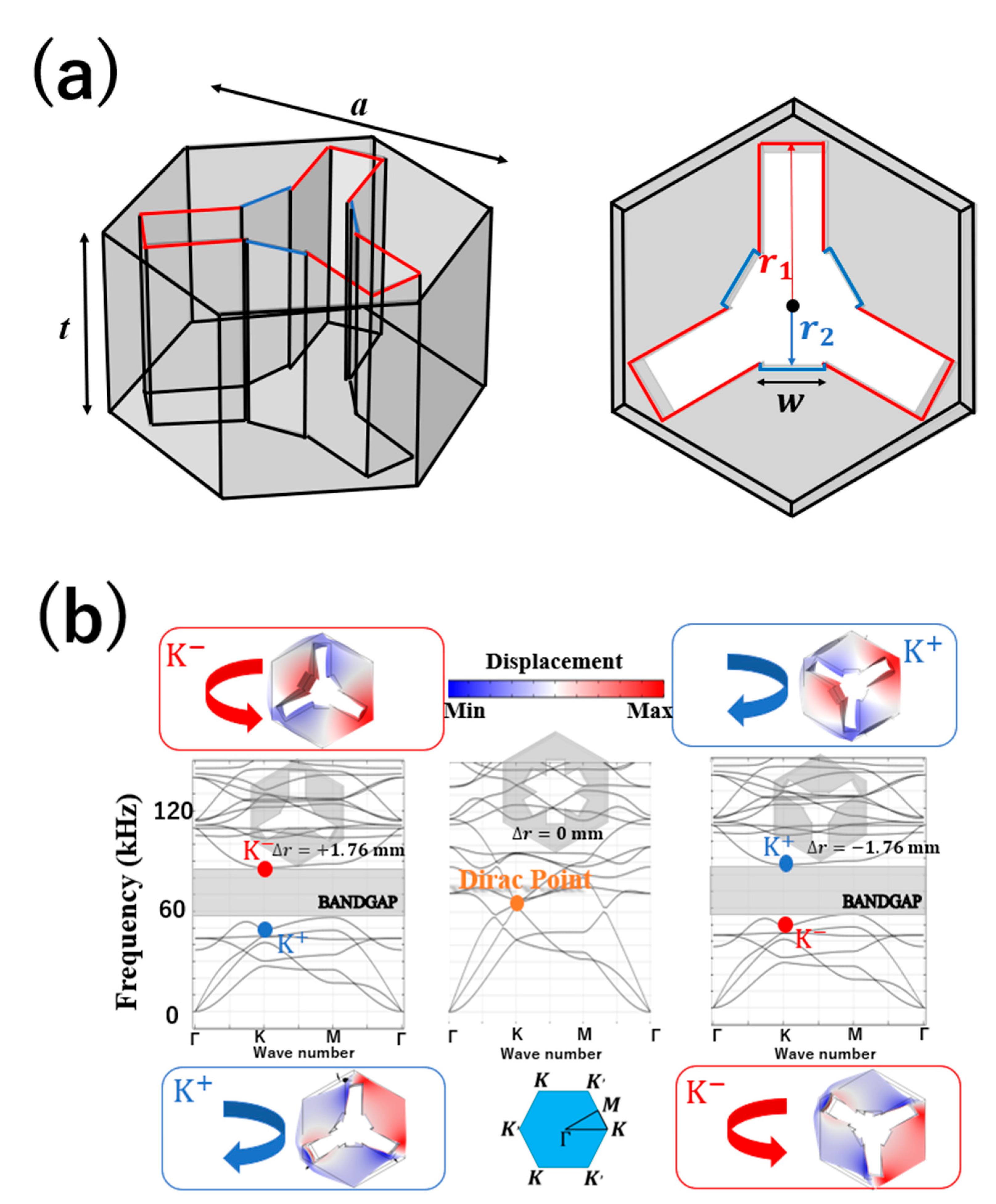
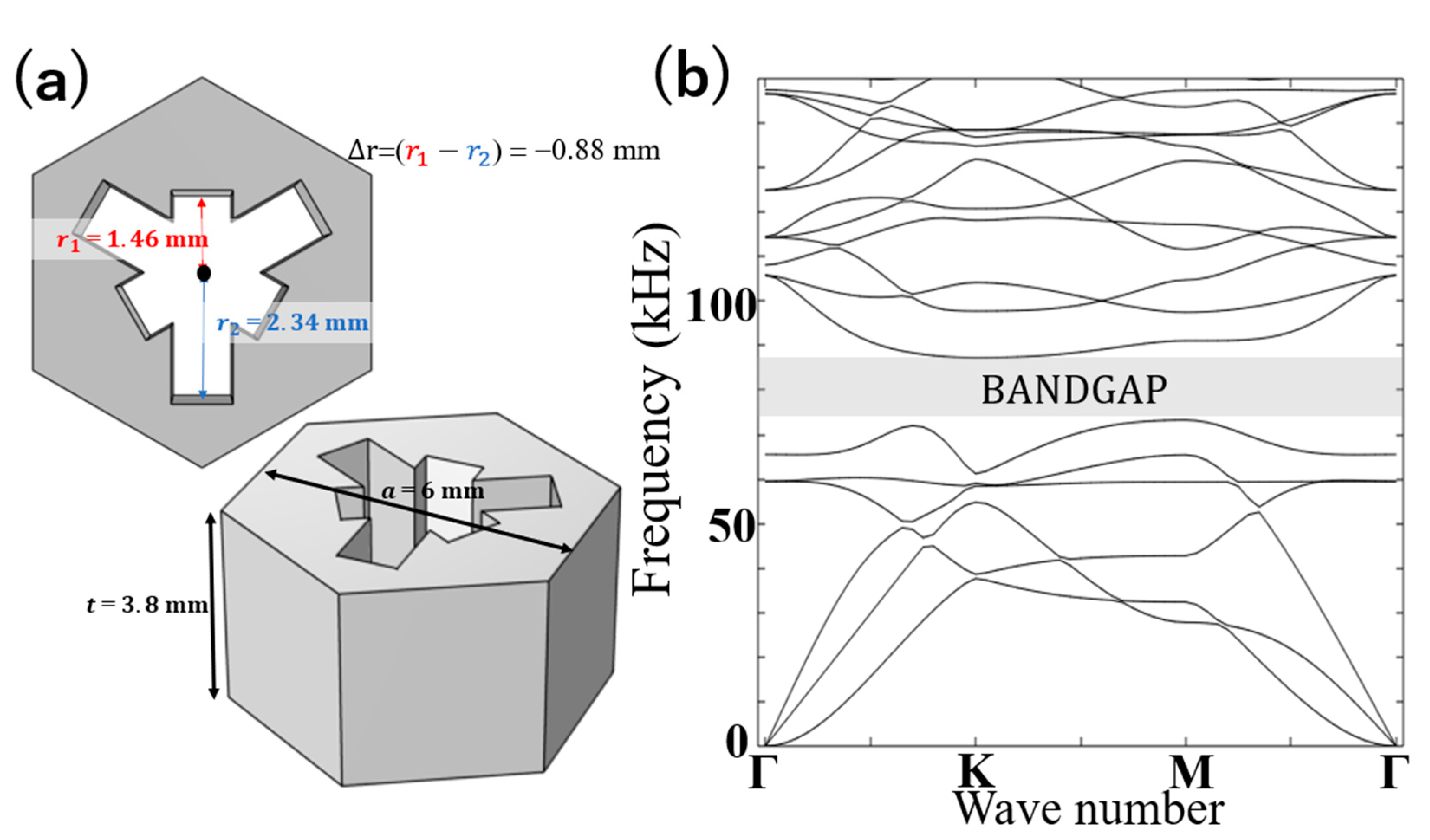
2.1. Optimization of Band Structure in Snowflake-like Phononic Crystal

The phononic structure adopted in this study consists of a three-dimensional unit cell with snowflake-shaped holes in a hexagonal grid. The valley-shaped band structure can be varied by changing the length of the six legs of the snowflake. Snowflake-like unit cells have been adopted in a variety of studies on phononic crystals as simple but highly controllable structural units for designing phonon band structures [32,33,34,35,36,37,38]. For example, D. Hatanaka et al. [37] suggest that a wide range of full bandgap appears around 0.3 GHz by optimizing snowflake-type phononic crystals in a GaAs membrane. Additionally, they fabricated a defect linear waveguide based on the designed phononic crystal and confirmed the presence or absence of the propagation modes. Furthermore, the phonons can be highly controllable by coupling them with a resonator adjacent to the waveguide. Masrura et al. [38] designed a snowflake-type phononic crystal that can control thermal phonons, which propagate at a much higher frequency than acoustic phonons. In this study, the authors reported that the size and position of the bandgap could be easily adjusted by changing the width of the branches of the snowflake structure. Furthermore, the transmission in the phononic crystals was indeed small within a wide bandgap frequency, whereas thermal phonons were conducted only in the frequency range outside the bandgap. Snowflake-type phononic crystals with high versatility have been actively used to control phonons in various frequency domains.
As shown in Figure 1a, the hexagonal lattice has dimensions with a lattice constant of a = 6 mm and a thickness of t = 3.8 mm. The snowflake-like scatterer has six legs with a width w = 1.1 mm, and the legs with lengths r1 (center-to-red outline) and r2 (center-to-blue outline) are alternatively arranged. The mirror symmetry of the unit cell can be broken by changing the difference between r1 and r2r = r2r1) while maintaining the total length constant. (We chose r1 + r2 = 3.8 mm so that each leg is precisely fabricated without touching/coalescing with each other.) In our design, the plate was made of polypropylene (PP), and the mass density, Young’s modulus, and Poisson’s ratio of PP were 900 kg/m3, 1.47 GPa, and 0.4, respectively. Numerical calculations on eigenmode analyses and elastic wave propagations were performed by solving the linear elastic wave equation for isotropic materials using the COMSOL Multiphysics software package [39] based on the finite element method (FEM).
First, the band structure was optimized by varying Δr. This is a novel choice of parameter for the structural change in contrast to the previous works that were based on structural change by rotation of the holes around the central axis normal to the plate [27,31]. A continuous decrease in Δr leads to the gap closing at Δr = 0 mm, forming a Dirac point, whereas a further decrease in Δr opens the gap again. Moreover, both K+ and K pseudo-spin modes appear above and below the gap between the K and K′ points in the Brillouin zone, respectively. Furthermore, by optimizing the crystal band diagram by varying Δr, the optimal structure with the widest bandgap topological phase transition was identified as Δr = ±1.76 mm. Figure 1b shows the band diagram of a phononic structure with a snowflake-shaped unit cell, revealing that the bandgap opens at Δr = +1.76 mm. Although the two eigenmodes have similar shapes, the vortex directions of the mechanical energy flow are opposite. Furthermore, the direction of the vortices changes above and below the band at Δr = 0. As this indicates a topological phase transition, valley chiral edge states might appear around this frequency [21]. From Figure 1b, the phonon-band topological phase transition was confirmed to occur in the reciprocal space and could be easily controlled using a single parameter Δr. In addition, the unit cell structure with an intermediate value of Δr (= −0.88 mm) demonstrated a bandgap (Figure 2a,b) ranging from 71.993 to 88.378 kHz. This gap width (16.385 kHz) was approximately 40% narrower than that in the unit cell with Δr = ±1.76 mm, and the gap width decreased as the value of Δr decreased. Furthermore, in supercells formed with intermediate values of Δr (±0.88 mm), the distance between the edge and bulk bands decreased as the gap width reduced. Consequently, the edge and bulk modes coexist at certain frequencies, preventing the efficient propagation of elastic waves through the edge mode. Therefore, a unit cell with Δr = +1.76 mm possessing the wider bandgap is required to design topological waveguides without degradation by a mixture of edge and bulk modes. As the bandgap increases, however, the Berry phases may not be well concentrated in the valleys [31,40]. This limits the gap size to an appropriate value for optimal design.

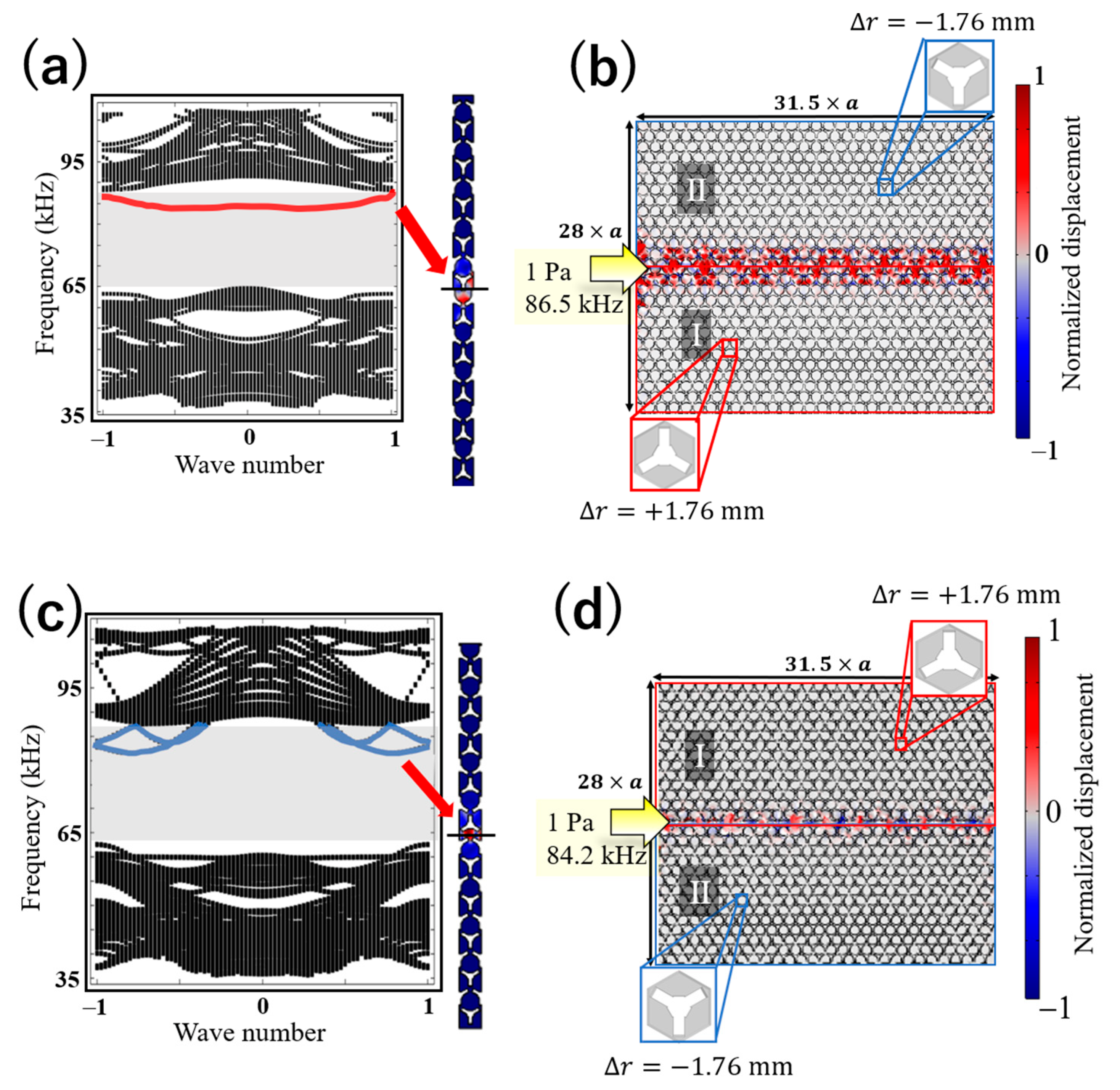
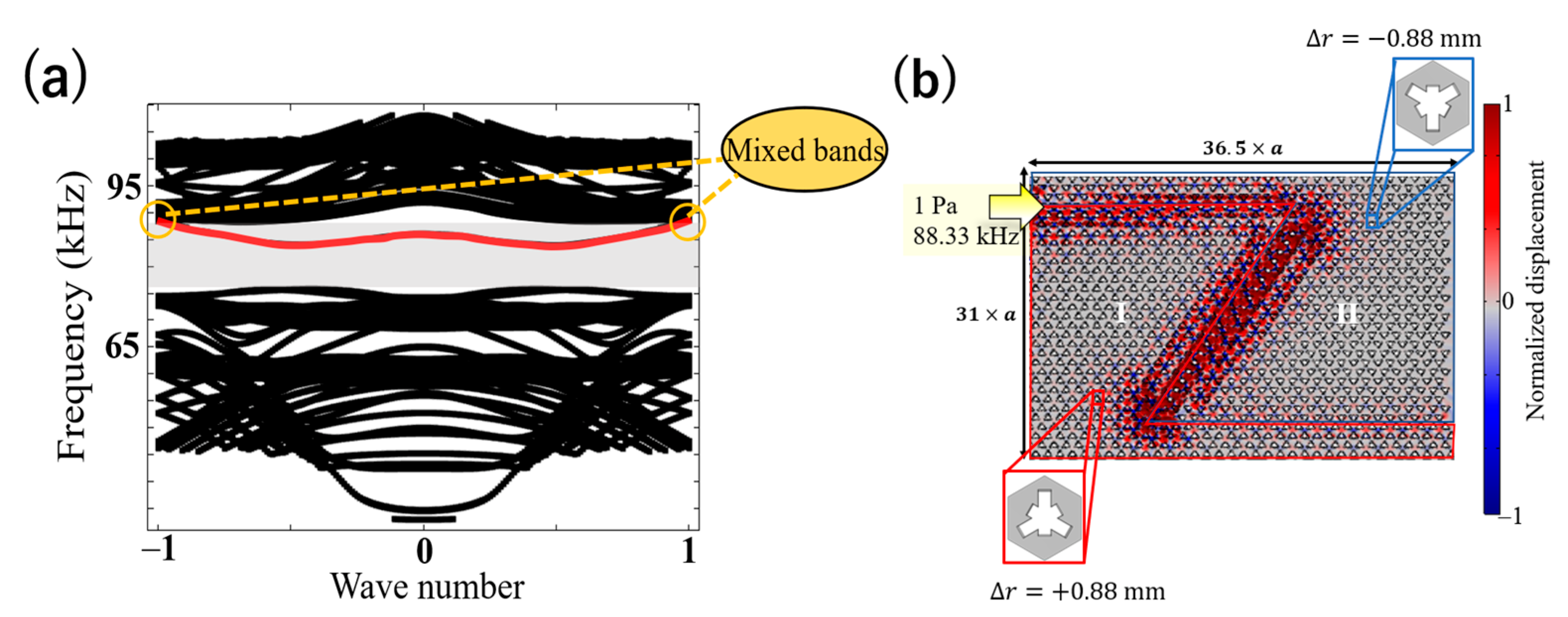
2.2. Excitation of Topological Edge Mode and Transmittance Analysis

Based on the above analysis, we calculated the phononic band structures and simulated the elastic wave propagations in a linear waveguide and a Z-shaped waveguide designed with a valley topological phononic structure. Figure 3 depicts the band diagrams for supercells of two topological phononic crystals along the kx direction and the out-of-plane displacement distribution in elastic wave propagation for an incident wave in linear waveguides. Figure 3a,b shows a band diagram for the supercell with Δr = +1.76 mm at the top (designated as “I”) and Δr = −1.76 mm at the bottom (“II”) and a linear waveguide designed with an array of the supercell (31(W) × 28(H) unit cells). Similarly, Figure 3c,d shows the band diagram for the supercell constructed with vertically exchanged unit cells and a linear waveguide designed with an array of supercells (31 × 28 unit cells). In Figure 3a, an edge mode, in which elastic waves propagate at the interfaces of the cells with different Δr (designated as “I–II”), appears between 85.838 and 86.774 kHz, as shown by the red lines. Similarly, in Figure 3c (for the interface “II–I”), an edge mode appears between 81.746 and 87.605 kHz, as indicated by the blue line. The displacement field in elastic waves with an incident pressure of 1 Pa is shown in Figure 3b,d. The incident frequencies for these simulations are 86.5 kHz in Figure 3b and 84.2 kHz in Figure 3d. Thus, the edge state of the topological acoustic was confirmed to be excited at the frequency estimated from the band diagrams in Figure 3a,c. The transmittances of the waveguides were measured by using a domain probe with a diameter of 1 mm. It was calculated from the absolute value of the amplitude of the maximum out-of-plane displacement among 10 points near the antinode in the wave profile for both the input and output ports. As a result, the transmittance was as high as 93% for the waveguide in Figure 3b and 92% for that in Figure 3d. In these simulations, as depicted in Figure 3b,d, the perfect match layer (PML) algorithm [41] was applied to eliminate reflection by the upper, lower, left, and right boundaries of the structures.
We further designed and examined a Z-shaped waveguide and its transmission properties for incident waves. As the interface along the oblique line in the Z shape has the same type of symmetry as that along the horizontal lines, these waveguides were used to assess the robustness of wave propagation against backscattering by the corners of the paths. Figure 4 illustrates the designed waveguides (36 × 31 unit cells) along the interfaces between a phononic structure with different Δr, Δr = +1.76 and −1.76 mm (I–II) in Figure 4a and inverted interface (II–I) in Figure 4b. The transmittance in these waveguides was also evaluated in a manner similar to the analysis of linear waveguides. As a result, the transmittance was as high as 90% in Figure 4a and 89% in Figure 4b. Thus, we confirmed that highly efficient elastic-wave transmission can be achieved even in a waveguide with corners, proving that the edge mode designed through the analysis of the topological phase transition in the phonon band diagram is topologically protected.
To demonstrate that the current numerical design also optimizes robustness, we performed a transmission analysis of the intermediate parameters Δr. Figure 5a shows the supercell band diagram with Δr = +0.88 mm at the top and Δr = −0.88 mm (I–II) at the bottom. Figure 5b shows the transmission analysis results of the Z-shaped waveguide excited with the 88.33 kHz edge mode shown in red, which appeared in the supercell analysis. It can be observed that the displacement near the end of the waveguide is smaller and blurred owing to the leakage of the wave into the bulk despite the edge mode. This can be attributed to the coupling of the edge mode with the bulk mode in the band (Figure 5a), as described in Section 2.1.

3. Fabrication and Wave-Transmission Measurement of Topological Phononic Waveguide in a Thin Plate

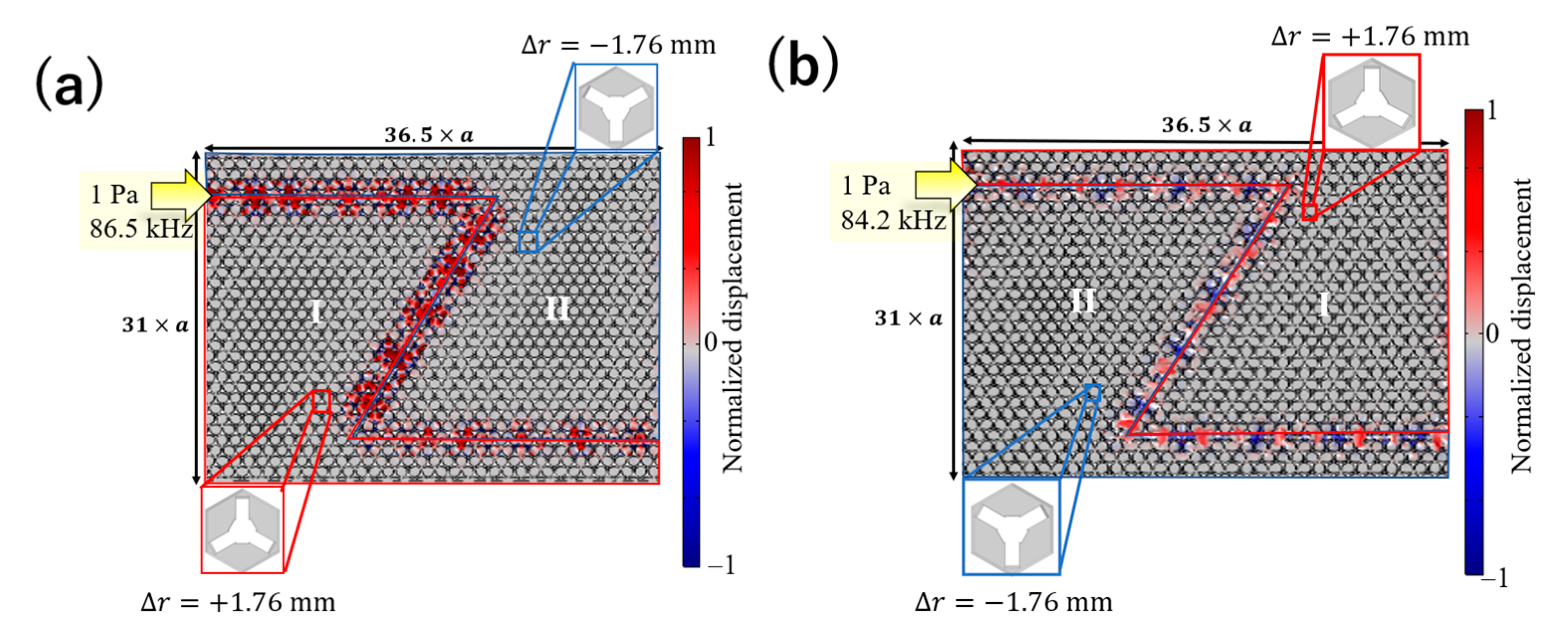
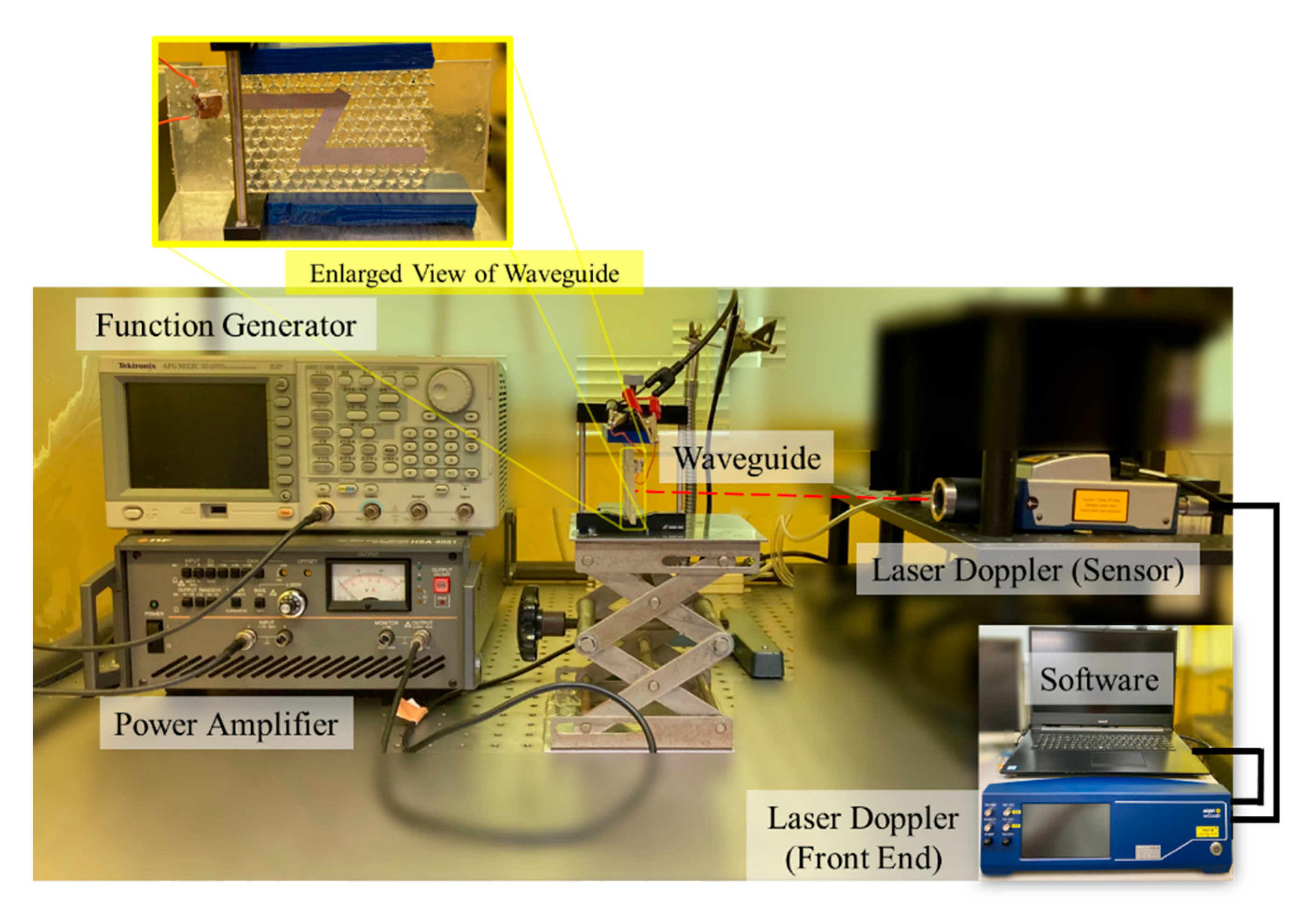
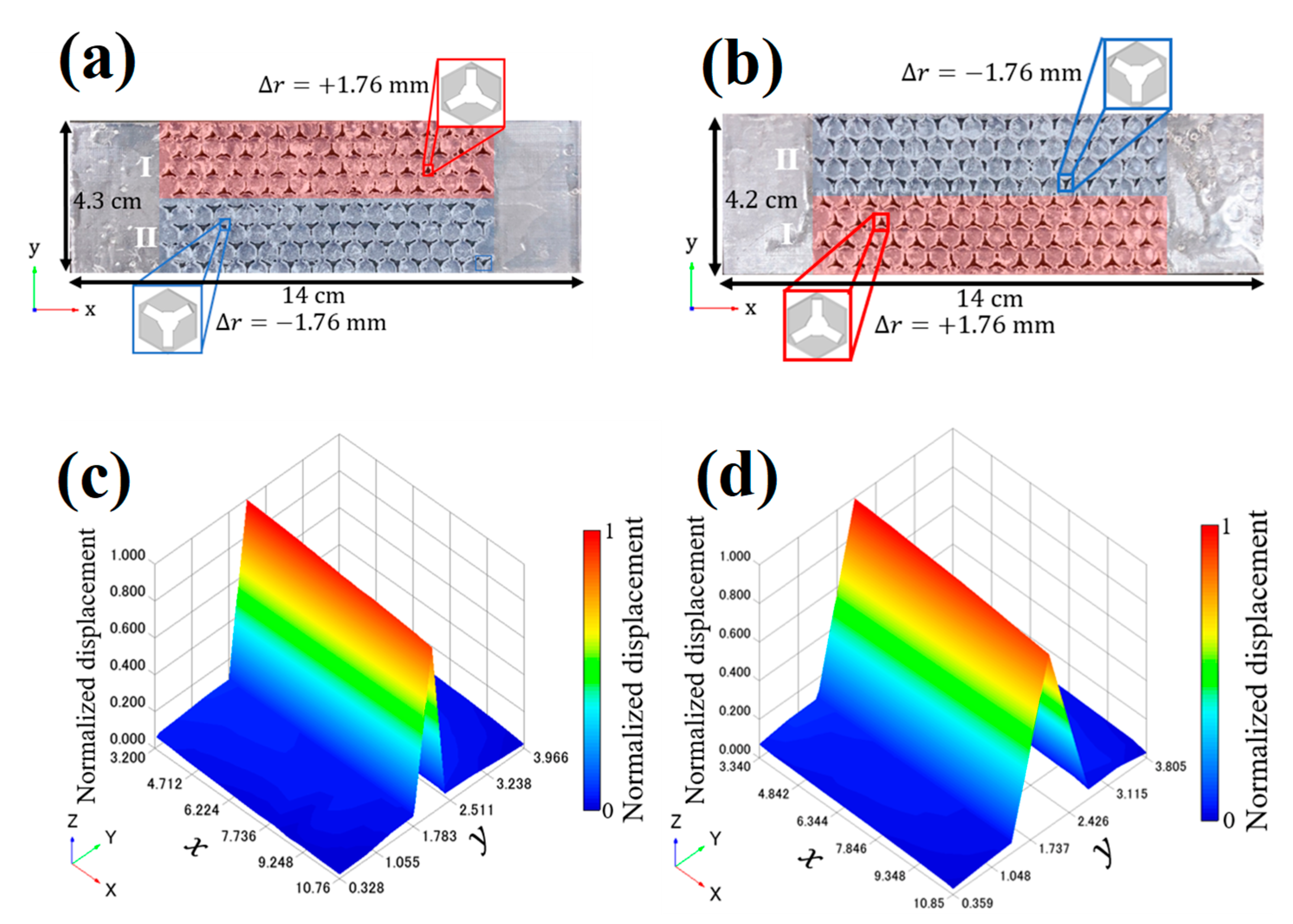
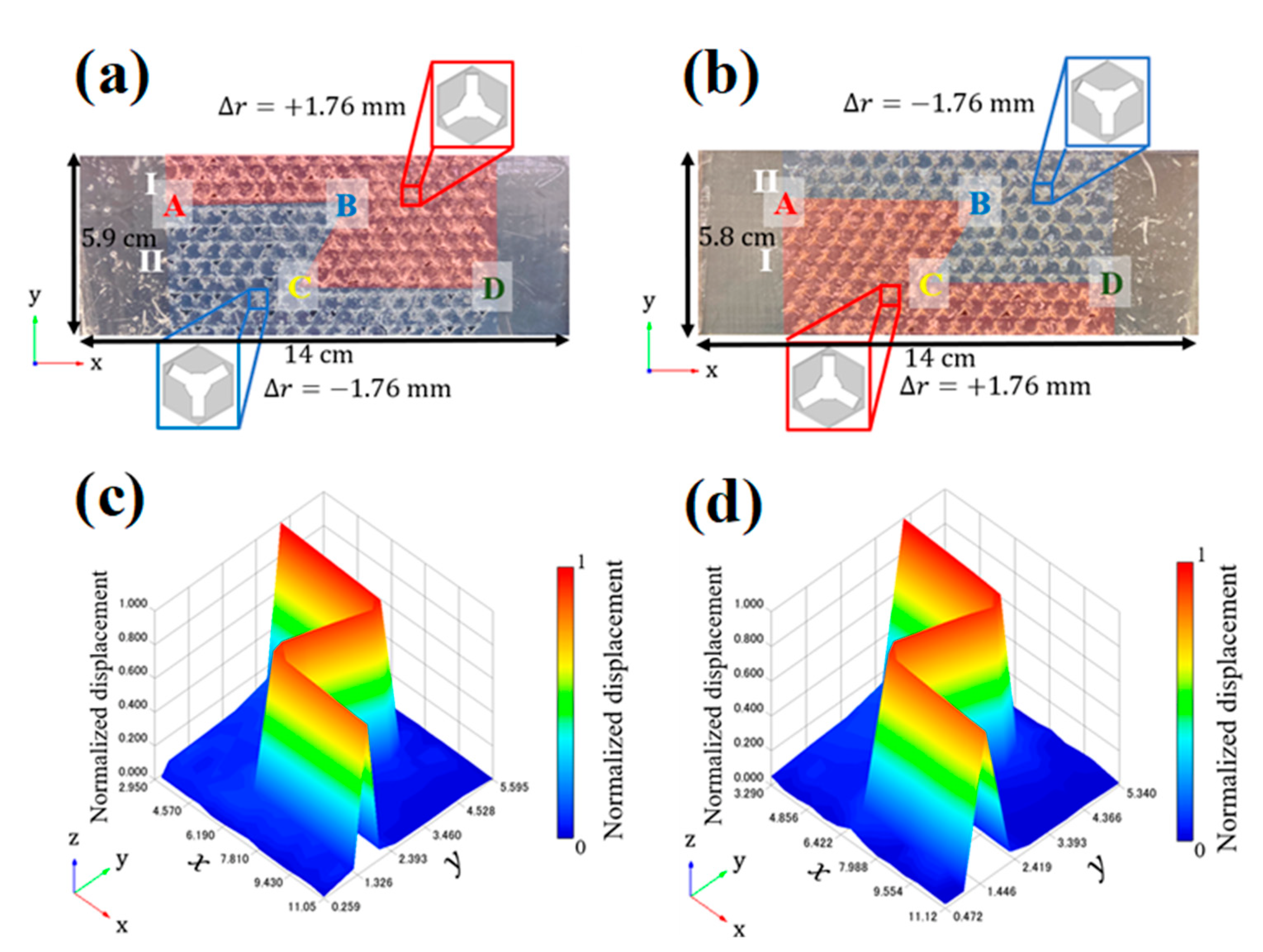
3.1. Fabricated Topological Linear and Z-Shaped Waveguides and Measurement of Out-of-Plane Displacement

Figure 6 shows the experimental setup for the measurement of elastic wave propagation. In the experiment, a continuous wave of 4.7 Vpp (peak-to-peak voltage) obtained from a function generator on the transmitting side was amplified to 188 Vpp using a power amplifier and converted into an elastic wave through a transducer. The induced elastic waves were measured and mapped using a laser-Doppler vibrometer. Unnecessary waves due to reflection from the edge of the plate were removed by attaching a sound-absorbing material to the sides. Figure 7 and Figure 8 include photographs of waveguide fabricated using a 3D printer (Form 3+ manufactured by Formlabs Co.) [42]. For a topological linear waveguide with a boundary between two phases (I–II), the displacement was measured at 140 points (Figure 7a), and for another type of interface (II-I), it was measured at 113 points (Figure 7b). The results are presented in Figure 7c,d. The values on the vertical axis in Figure 7c,d are the amplitudes of the out-of-plane displacement normalized by the amplitude at the points near the incident wave. Similar to the numerical simulations in Figure 3b,d, a large displacement can be observed only along the interfaces.
Next, topological Z-shaped waveguides were fabricated in the same manner as the straight waveguide. The dimensions of the samples were 15 × 11 unit cells. The boundary between the two phases (I–II) exists in a Z-shaped path, as shown by the boundary between the differently colored regions in Figure 8a. Similarly, another type of interface (II–I) was fabricated, as shown in Figure 8b. The displacement at 187 points was measured in the topological Z-guide with a boundary between the two phases (I–II), and that at 155 points in another type of interface (II–I). Figure 8c,d depicts the spatial distribution of the displacement. In interface types, a large displacement was observed only along the interface regions, indicating that highly efficient wave propagation was realized, as predicted by the numerical simulations shown in Figure 4a,b. These results reveal that the possible frequency of the edge mode excitation is 86.5 kHz for the I–II interface and 84.2 kHz for the II–I interface. Furthermore, transmittance was calculated based on the results obtained from the displacements measured using the laser Doppler vibrometer. Here, transmittance is defined as the ratio of the measured out-of-plane displacement (absolute values) at the end of the waveguide to that near the point where the incident wave is emitted.

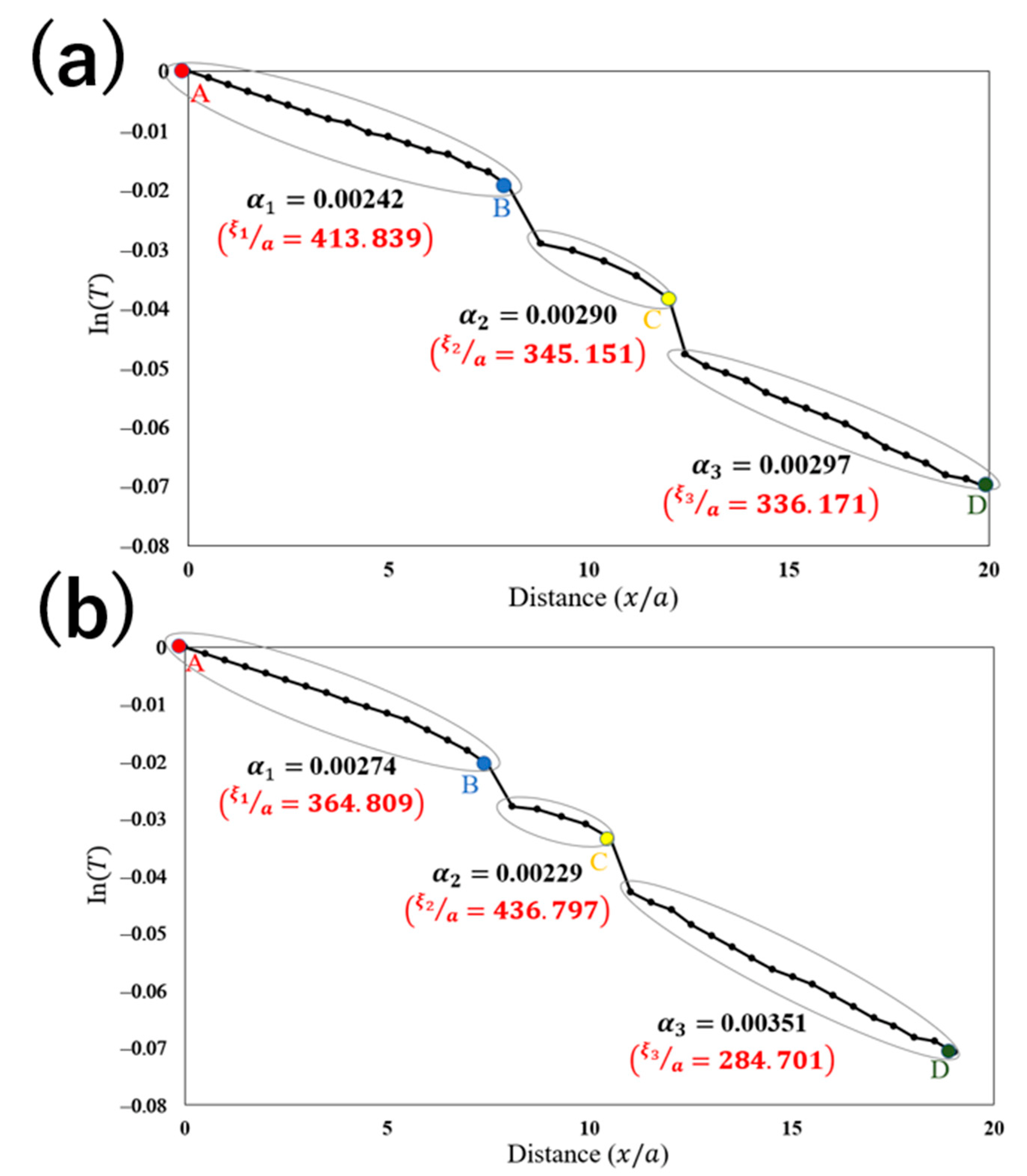
3.2. Analyses on Transmittance and Backscattering Length

Table 1 summarizes the results of transmittance for each topological elastic waveguide obtained by experimental measurements and FEM analysis. It can be seen from the table that the experimentally obtained transmittances of all waveguides were slightly smaller than those obtained from the numerical results. One of the reasons for this systematic degradation in the transmittance obtained in the experiment is that the FEM analysis assumed no material loss owing to the elastic vibration in this frequency range. For comparison, we confirmed this effect by performing an additional simulation of the edge-mode propagation in a topological straight waveguide with an isotropic loss of 0.005, which is the typical value of the material. We found that the transmittance decreased by approximately 2% owing to this effect. The remaining discrepancy between the experiments and simulations may be attributed to the unknown frequency dependence of the loss factor, particularly at high frequencies. We also observed that the transmission of the Z-shaped waveguide was approximately 5% lower than that of a straight waveguide. Recently, such degradation of robustness in the presence of corners and/or structural randomness has been quantitatively evaluated in terms of the “backscattering length” ξ in valley topological photonic waveguides [43,44,45]. The same evaluation is valid in terms of ξ for the valley topological phononic waveguide. Figure 9a,b shows logarithmic plots of the transmittance (T) along the paths of the Z-shaped waveguides in the experiment. The points designated by A, B, C, and D in Figure 9a,b correspond to the points in Figure 8a,b. The negative inverse of the slope of the graphs defines the backscattering length ξ. The values of ξ were evaluated for each segment AB and CD to provide approximately 414a and 336a (a = 3.8 mm is the lattice constant), respectively, at the II–I interface and 437a and 285a, respectively, at the I–II interface. However, at B and C (corners in the waveguides), a smaller ξ (~100) than the former was observed. This indicates that the effect of backscattering in the corner sections is more pronounced than the structural randomness in the straight sections. The reason for the lower values of the Z-shaped topological waveguide than those of the straight topological waveguide was thereby identified quantitatively.
The origin of the larger loss at corners may reflect the characteristics of the edge state in the present structures. As mentioned in Section 2.1, the valley topological phase in wide bandgap can be less localized, which weakens the robustness. Additionally, the edge bands depicted in Figure 3 are rather nondispersive (not crossing over the gap). Hence, these cases may be classified as weak topological states [40,46]. The immunization of backscattering was thereby degraded. Nevertheless, the present values of approximately 400a in straight waveguides prove eminent efficiency compared with the reported values (~100a) in valley-topological photonic systems [44,45].

4. Conclusions

We designed valley-type topological phononic crystals in plastic plates, in which the topological phase transition of the phonon band occurs by changing the structural parameters. A snowflake-type unit cell structure was employed as a simple but highly controllable structural unit for designing the phonon band structure. By varying Δr, we optimized the band structure and designed linear and Z-shaped topological waveguides with topological interfaces using two types of unit cells with Δr = ± 1.76 mm. The appearance of edge states for efficient elastic wave propagation was demonstrated using 3D finite element method (FEM) simulations. Observation of the out-of-plane displacement distribution at the interface and the transmission analysis of the designed waveguides with linear and Z-shaped paths proved highly efficient and robust elastic wave propagation via topologically protected edge modes. On the other hand, the intermediate structures with Δr = ± 0.88 mm showed that the propagation loss became significant owing to the appearance of a narrow bandgap and the mixing of the edge mode with the bulk ones, revealing that the precise design of the gap width is important for realizing edge mode propagation. On the basis of these numerical analyses, both linear and Z-shaped topological waveguides (Δr = ± 1.76 mm) were fabricated using a 3D printer. Transmission measurements were performed to show that the fabricated topological waveguide has high efficiency and robustness in elastic wave propagation at approximately 85 kHz. In addition, we quantitatively identified the magnitude and sources of the transmission loss in terms of the backscattering length estimated from the decaying behavior of the displacement field distributions along the paths. The results revealed that predominant loss was observed at the corners, whereas an extremely low loss (large values of the backscattering length) was estimated in the other straight segments in the topological interfaces. This can be attributed to the fact that the edge modes depicted in Figure 3 have appeared without crossing over the gap, implying the edge states weakly topological [46]. Nevertheless, the backscattering lengths estimated here give promises for practical device applications.
In summary, the present study showed that the structural design based on the band topology of snowflake-type topological phononic crystals can be applied to highly efficient elastic-wave devices as alternative and/or complementary components for information carriers in next-generation communication platforms.

Author Contributions

Conceptualization, M.K. and K.T.; computation and experiment, M.K.; validation, M.M. and K.T.; writing—original draft preparation, M.K.; writing—review and editing, M.K., M.M. and K.T.; visualization, M.K.; project administration, K.T.; funding acquisition, K.T. All authors have read and agreed to the published version of the manuscript.

Funding

This research was funded by Japan Society for the Promotion of Science grant number JP21H05020 and JP21K18877.

Institutional Review Board Statement

Not applicable.

Informed Consent Statement

Not applicable.

Data Availability Statement

Not applicable.

Conflicts of Interest

The authors declare no conflict of interest.

References

  1. Kushwaha, M.S.; Halevi, P.; Dobrzynski, L.; Djafari-Rouhani, B. Acoustic Band Structure of Periodic Elastic Composites. Phys. Rev. Lett. 1993, 71, 2022–2025. [Google Scholar] [CrossRef]
  2. Khelif, A.; Choujaa, A.; Benchabane, S.; Djafari-Rouhani, B.; Laude, V. Guiding and bending of acoustic waves in highly confined phononic crystal waveguides. Appl. Phys. Lett. 2004, 84, 4400–4402. [Google Scholar] [CrossRef]
  3. Pennec, Y.; Djafari-Rouhani, B.; Vasseur, J.O.; Khelif, A.; Deymier, P.A. Tunable filtering and demultiplexing in phononic crystals with hollow cylinders. Phys. Rev. E 2004, 69, 046608. [Google Scholar] [CrossRef] [PubMed] [Green Version]
  4. Sun, J.-H.; Wu, T.-T. Analyses of mode coupling in joined parallel phononic crystal waveguides. Phys. Rev. B 2005, 71, 174303. [Google Scholar] [CrossRef]
  5. Matsuda, O.; Wright, O.B. Phononic Crystals; Khelif, A., Adibi, A., Eds.; Springer: New York, NY, USA, 2016; p. 191. [Google Scholar]
  6. Wu, L.-Y.; Chen, L.-W.; Liu, C.-M. Acoustic energy harvesting using resonant cavity of a sonic crystal. Appl. Phys. Lett. 2009, 96, 013506. [Google Scholar] [CrossRef]
  7. Liu, Z.; Zhang, X.; Mao, Y.; Zhu, Y.Y.; Yang, Z.; Chan, C.T.; Sheng, P. Locally resonant sonic materials. Science 2000, 289, 1734–1736. [Google Scholar] [CrossRef] [PubMed]
  8. Zhao, D.; Ye, Y.; Xu, S.; Zhu, X.; Yi, L. Broadband and wide-angle negative reflection at a phononic crystal boundary. Appl. Phys. Lett. 2014, 104, 043503. [Google Scholar] [CrossRef]
  9. Hatanaka, D.; Yamaguchi, H. Mode-sensitive magnetoelastic coupling in phononic-crystal magnomechanics. APL Mater. 2021, 9, 071110. [Google Scholar] [CrossRef]
  10. Workie, T.B.; Wu, T.; Bao, J.-F.; Hashimoto, K. Design for high-quality factor of piezoelectric-on-silicon MEMS resonators using resonant plate shape and phononic crystals. Jpn. J. Appl. Phys. 2021, 60, SDDA03. [Google Scholar] [CrossRef]
  11. Hikata, R.; Tsuruta, K.; Ishikawa, A.; Fujimori, K. Terahertz acoustic wave on piezoelectric semiconductor film via large-scale molecular dynamics simulation. Jpn. J. Appl. Phys. 2015, 54, 07HB07. [Google Scholar] [CrossRef]
  12. Li, X.; Liu, Z. Bending and branching of acoustic waves in two-dimensional phononic crystals with linear defects. Phys. Lett. A 2005, 338, 413–419. [Google Scholar] [CrossRef]
  13. Manabe, K.; Ishikawa, A.; Yamamoto, K.; Kanda, T.; Tsuruta, K. Design and Assessment of Phononic Crystals for Controlling Ultrasonic Wave via Optical Measurement Method. In Proceedings of the 2018 IEEE International Ultrasonics Symposium (IUS), Kobe, Japan, 22–25 October 2018; p. 8580129. [Google Scholar]
  14. Deng, Y.; Ge, H.; Tian, Y.; Lu, M.; Jing, Y. Observation of zone folding induced acoustic topological insulators and the role of spin-mixing defects. Phys. Rev. B 2017, 96, 184305. [Google Scholar] [CrossRef] [Green Version]
  15. Ma, G.; Xiao, M.; Chan, C.T. Topological phases in acoustic and mechanical systems. Nat. Rev. Phys. 2019, 1, 281. [Google Scholar] [CrossRef]
  16. Moore, J.E. The birth of topological insulators. Nature 2010, 464, 194–198. [Google Scholar] [CrossRef]
  17. Hatsugai, Y. Chem Number and Edge States in the Integer Quantum Hall Effect. Phys. Rev. Lett. 1993, 71, 3697–3700. [Google Scholar] [CrossRef]
  18. Jia, D.; Sun, H.-X.; Xia, J.-P.; Yuan, S.-Q.; Liu, X.-J.; Zhang, C. Acoustic topological insulator by honeycomb sonic crystals with direct and indirect band gaps. New J. Phys. 2018, 20, 093027. [Google Scholar] [CrossRef] [Green Version]
  19. Mei, J.; Chen, Z.; Wu, Y. Pseudo-time-reversal symmetry and topological edge states in two dimensional acoustic crystals. Sci. Rep. 2016, 6, 32752. [Google Scholar] [CrossRef] [PubMed] [Green Version]
  20. Yu, S.-Y.; He, C.; Wang, Z.; Liu, F.-K.; Sun, X.-C.; Li, Z.; Lu, H.-Z.; Lu, M.-H.; Liu, X.-P.; Chen, Y.-F. Elastic pseudospin transport for integratable topological phononic circuits. Nat. Commun. 2018, 9, 3072. [Google Scholar] [CrossRef] [PubMed] [Green Version]
  21. Lu, J.; Qiu, C.; Ye, L.; Fan, X.; Ke, M.; Zhang, F.; Liu, Z. Observation of topological valley transport of sound in sonic crystals. Nat. Phys. 2017, 13, 369. [Google Scholar] [CrossRef] [Green Version]
  22. Yan, M.; Lu, J.; Li, F.; Deng, W.; Huang, X.; Ma, J.; Liu, Z. On-chip valley topological materials for elastic wave manipulation. Nat. Mater. 2018, 17, 993. [Google Scholar] [CrossRef]
  23. Zhang, Z.; Tian, Y.; Cheng, Y.; Wei, Q.; Liu, X.; Christensen, J. Topological Acoustic Delay Line. Phys. Rev. Appl. 2018, 9, 034032. [Google Scholar] [CrossRef] [Green Version]
  24. Han, X.; Peng, Y.-G.; Li, L.; Hu, Y.; Mei, C.; Zhao, D.-G.; Zhu, X.-F.; Wang, X. Experimental Demonstration of Acoustic Valley Hall Topological Insulators with the Robust Selection of C3v-Symmetric Scatterers. Phys. Rev. Appl. 2019, 12, 014046. [Google Scholar] [CrossRef]
  25. Huo, S.-Y.; Chen, J.-J.; Huang, H.-B.; Huang, G.-L. Pseudospins and topological edge states in elastic shear waves. Sci. Rep. 2017, 7, 10335. [Google Scholar] [CrossRef] [PubMed]
  26. Song, A.; Li, J.; Shen, C.; Chen, T.; Cummer, S.A. Switchable directional sound emission with improved field confinement based on topological insulations. Appl. Phys. Lett. 2020, 117, 043503. [Google Scholar] [CrossRef]
  27. Okuno, K.; Tsuruta, K. Topologically robust sound wave transport in two-dimensional phononic crystal with a circular rod arrangement in water. Jpn. J. Appl. Phys. 2020, 59, SKKA05. [Google Scholar] [CrossRef]
  28. Cha, I.; Kim, K.W.; Daraio, C. Experimental realization of on-chip topological nanoelectromechanical metamaterials. Nature 2018, 564, 229. [Google Scholar] [CrossRef]
  29. Ma, J.; Xi, X.; Sun, X. Experimental Demonstration of Dual-Band Nano-Electromechanical Valley-Hall Topological Metamaterials. Adv. Mater. 2021, 33, 2006521. [Google Scholar] [CrossRef] [PubMed]
  30. Zhang, Q.; Lee, D.; Zheng, L.; Ma, X.; Meyer, S.I.; He, L.; Ye, H.; Gong, Z.; Zhen, B.; Lai, K.; et al. Gigahertz topological valley Hall effect in nanoelectromechanical phononic crystals. Nat. Electron. 2022, 5, 157. [Google Scholar] [CrossRef]
  31. Kim, I.; Arakawa, Y.; Iwamoto, S. Design of GaAs-based valley phononic crystals with multiple complete phononic bandgaps at ultra-high frequency. Appl. Phys. Exp. 2019, 12, 047001. [Google Scholar] [CrossRef]
  32. Safavi-Naeini, A.H.; Hill, J.T.; Meenehan, S.; Chan, J.; Gröblacher, S.; Painter, O. Two-Dimensional Phononic-Photonic Band Gap Optomechanical Crystal Cavity. Appl. Phys. Lett. 2014, 112, 153603. [Google Scholar] [CrossRef] [PubMed]
  33. Baboly, M.G.; Reinke, C.M.; Griffin, B.A.; El-Kady, I.; Leseman, Z.C. Acoustic waveguiding in a silicon carbide phononic crystals at microwave frequencies. Appl. Phys. Lett. 2018, 112, 103504. [Google Scholar] [CrossRef]
  34. Brendel, C.; Peano, V.; Painter, O.; Marquardt, F. Snowflake phononic topological insulator at the nanoscale. Phys. Rev. B. 2018, 97, 020102. [Google Scholar] [CrossRef] [Green Version]
  35. Luo, J.; Feng, L.; Huang, H.; Chen, J. Pseudomagnetic fields and Landau levels for out-of-plane elastic waves in gradient snowflake-shaped crystal. Phys. Lett. A 2019, 38, 125974. [Google Scholar] [CrossRef]
  36. Liu, S.; Tong, H.; Fang, K. Optomechanical crystal with bound states in the continuum. Nat. Commun. 2020, 13, 3187. [Google Scholar] [CrossRef] [PubMed]
  37. Hatanaka, D.; Yamaguchi, H. Real-Space Characterization of Cavity-Coupled Waveguide Systems in Hypersonic Phononic Crystals. Phys. Rev. Appl. 2020, 13, 024005. [Google Scholar] [CrossRef] [Green Version]
  38. Masrura, H.M.; Kareekunnan, A.; Liu, F.; Ramaraj, S.G.; Ellrott, G.; Hammam, A.M.M.; Muruganathan, M.; Mizuta, H. Design of Graphene Phononic Crystals for Heat Phonon Engineering. Micromachines 2020, 11, 655. [Google Scholar] [CrossRef] [PubMed]
  39. COMSOL Multiphysics® www.comsol.com. COMSOL AB: Stockholm, Sweden. Available online: https://www.comsol.jp/forum/thread/150662/Citing-COMSOL-in-publications (accessed on 21 September 2022).
  40. Zhang, F.; Allan, H.M.; Eugene, J.M. Valley Chern numbers and boundary modes in gapped bilayer graphene. Proc. Natl. Acad. Sci. USA 2013, 110, 1054. [Google Scholar] [CrossRef] [PubMed] [Green Version]
  41. Yuan, X.; Borup, D.; Wiskin, J.W.; Berggren, M.; Eidens, R.; Johnson, S.A. Formulation and Validation of Berenger’s PML Absorbing Boundary for the FDTD Simulation of Acoustic Scattering. IEEE Trans. Ultrason. Ferroelectr. Freq. Control 1997, 44, 816. [Google Scholar] [CrossRef]
  42. Kataoka, M.; Misawa, M.; Tsuruta, K. Design and measurement of topological elastic waveguide based on phononic crystal. Proc. Symp. Ultrason. Electron. 2021, 42, 1J1-1. [Google Scholar]
  43. Orazbayev, B.; Fleury, R. Quantitative robustness analysis of topological edge modes in C6 and valley-Hall metamaterial waveguides. Nanophotonics 2019, 8, 1433. [Google Scholar] [CrossRef]
  44. Arregui, G.; Gomis-Bresco, J.; Sotomayor-Torres, C.M.; Garcia, P.D. Quantifying the Robustness of Topological Slow Light. Phys. Rev. Lett. 2021, 126, 027493. [Google Scholar] [CrossRef] [PubMed]
  45. Patterson, M.; Hughes, S. Disorder-Induced Coherent Scattering in Slow-Light Photonic Crystal Waveguide. Phys. Rev. Lett. 2009, 102, 253903. [Google Scholar] [CrossRef] [PubMed] [Green Version]
  46. Qi, X.-L.; Zhang, S.-C. Topological insulators and superconductors. Rev. Mod. Phys. 2011, 83, 1057. [Google Scholar] [CrossRef]
Figure 1. (a) Snowflake-like unit-cell structure in a phononic crystal and (b) phonon band diagrams and eigenmodes at K points for three unit-cell structures with different Δr.
Symmetry 14 02133 g001
Figure 2. (a) Snowflake-like unit-cell structure in an intermediate phononic crystal and (b) its phonon band diagram.
Symmetry 14 02133 g002
Figure 3. (a) Band diagram of the supercell with the I–II interface and (b) a linear waveguide designed with an array (31 columns) of the supercell. (c,d): The same as in (a,b), respectively, but for the supercell with the II–I interface. (Wave numbers in (a,c) are in unit of π/a).
Symmetry 14 02133 g003
Figure 4. Structures and displacement fields for incident wave at 84.2 kHz in Z-shaped topological waveguides designed with (a) I–II and (b) II–I interfaces, respectively, between the unit cells of Δr = ± 1.76 mm.
Symmetry 14 02133 g004
Figure 5. (a) Band diagram of the intermediate supercell with the I–II interface and (b) Z-shaped waveguide designed with an array of the supercell. (Wave numbers in (a) are in unit of π/a).
Symmetry 14 02133 g005
Figure 6. Experimental system: The electrical signal output from the function generator is amplified by a power amplifier. The electrical signal is converted to elastic wave via a piezoelectric transducer attached to the fabricated waveguide. The out-of-plane displacement of the surface acoustic wave propagating through the waveguide is measured using a laser Doppler vibrometer (VIO-130 manufactured by Polytec GmbH).
Symmetry 14 02133 g006
Figure 7. Linear valley topological waveguides with (a) the II–I interface and (b) I–II interface. (c,d) depict distributions of normalized displacement.
Symmetry 14 02133 g007
Figure 8. Z-shaped valley topological waveguides with (a) the II–I interface and (b) I–II interface. (c,d) depict distributions of normalized displacement. (See text for what A–D in (a,b) denote).
Symmetry 14 02133 g008
Figure 9. Logarithmic plots of the transmittance (T) along the paths of the Z-shaped waveguides (a) with the II–I interface and (b) with the I–II interface.
Symmetry 14 02133 g009
Table 1. Transmittance of four types of topological elastic waveguide.
Type of WaveguideSimulationExperiment
Linear waveguide (I–II)93%89%
Linear waveguide (II–I)92%90%
Z-shaped waveguide (I–II)90%85%
Z-shaped waveguide (II–I)89%85%
Publisher’s Note: MDPI stays neutral with regard to jurisdictional claims in published maps and institutional affiliations.

