

Process Parameters and Geometry Effects on Piezoresistivity in Additively Manufactured Polymer Sensors


Abstract
1. Introduction
2. Materials and Methods
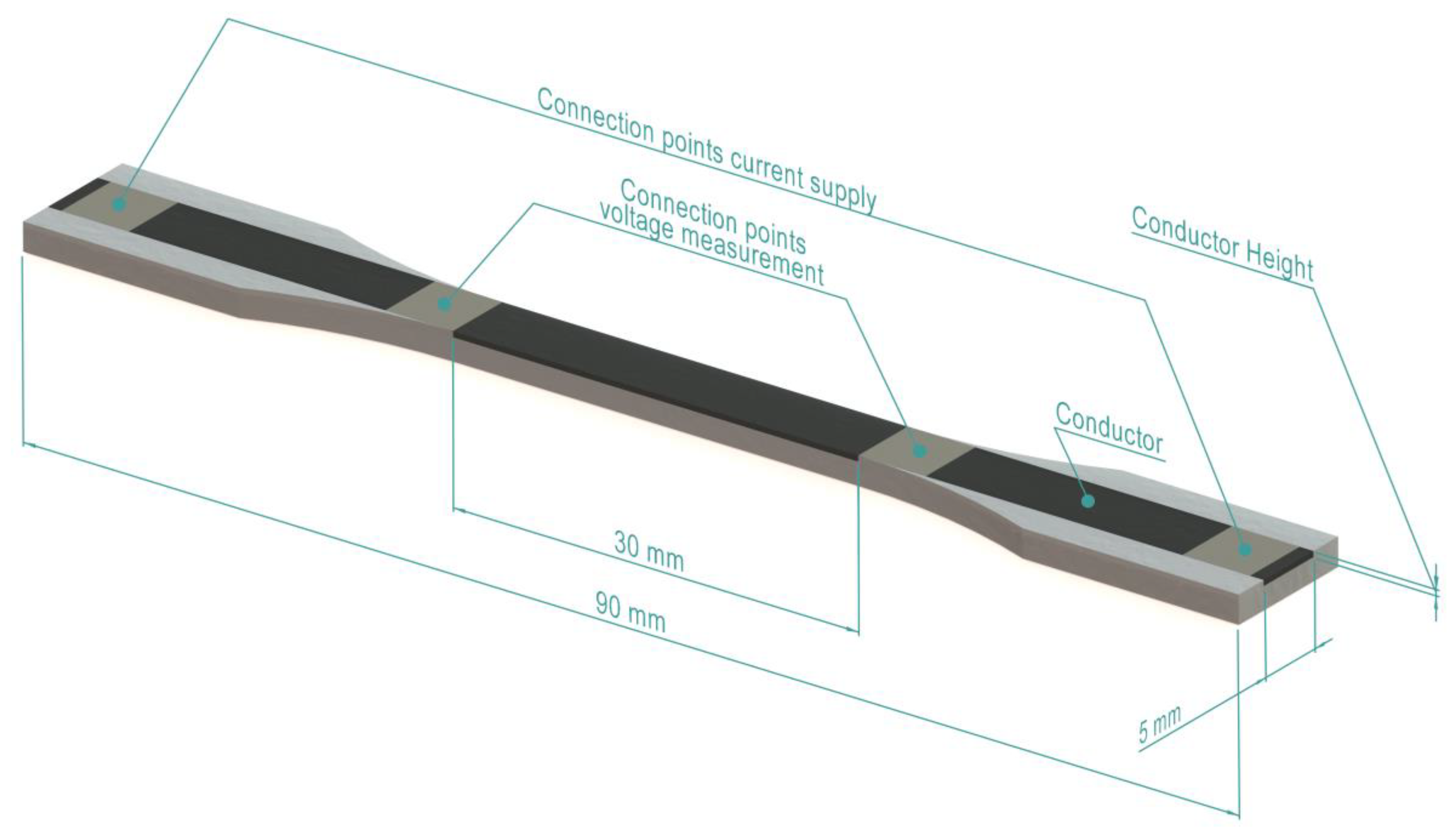
2.1. Sensor Design and AM Setup
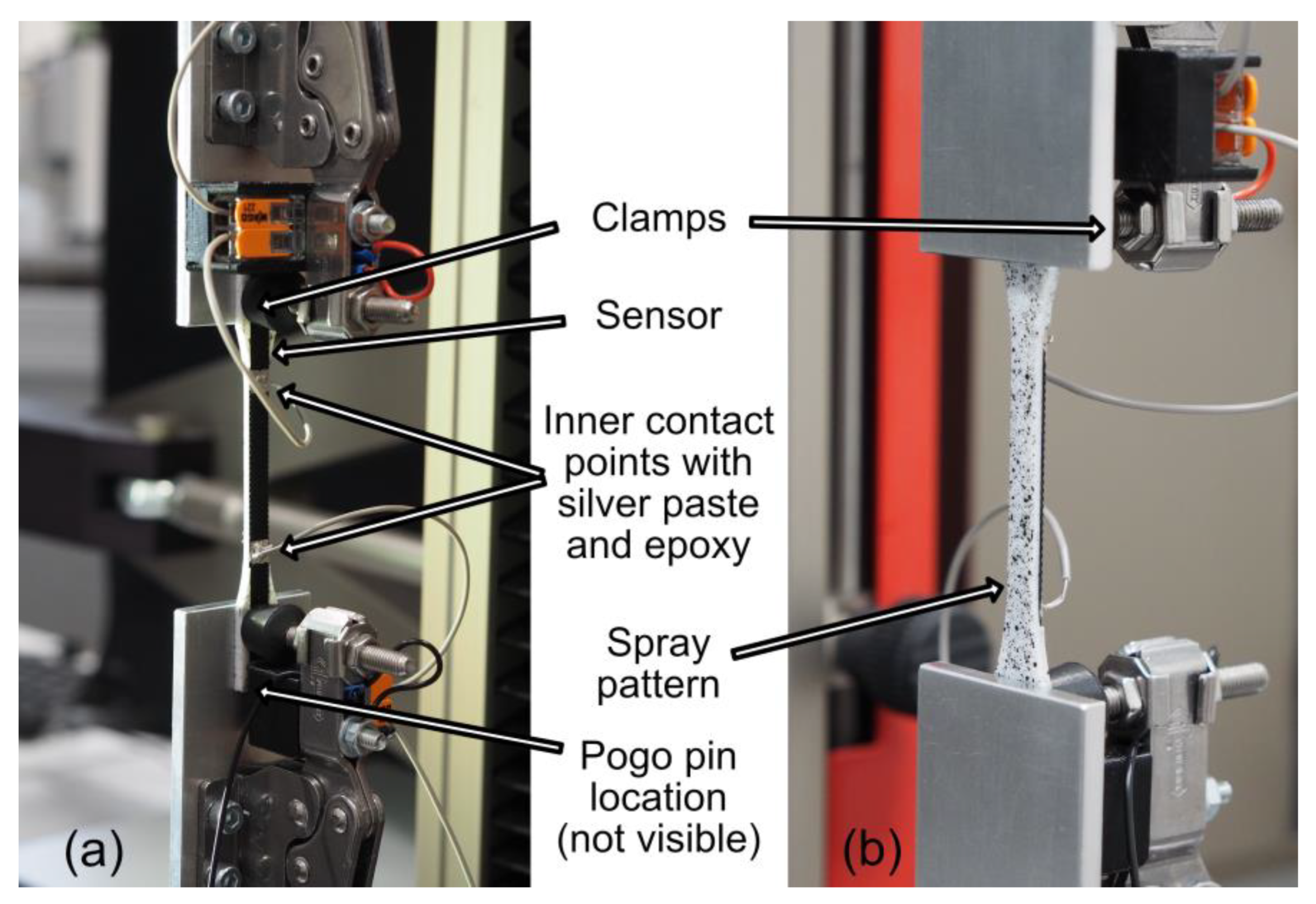
2.2. Measurement Setup
2.3. Data Analysis Method
- The initial resistance R0 for each sensor in the unloaded state.
- The sensor sensitivity, as expressed by the dimensionless gauge factor (GF), according to the following equation [46]:
3. Results
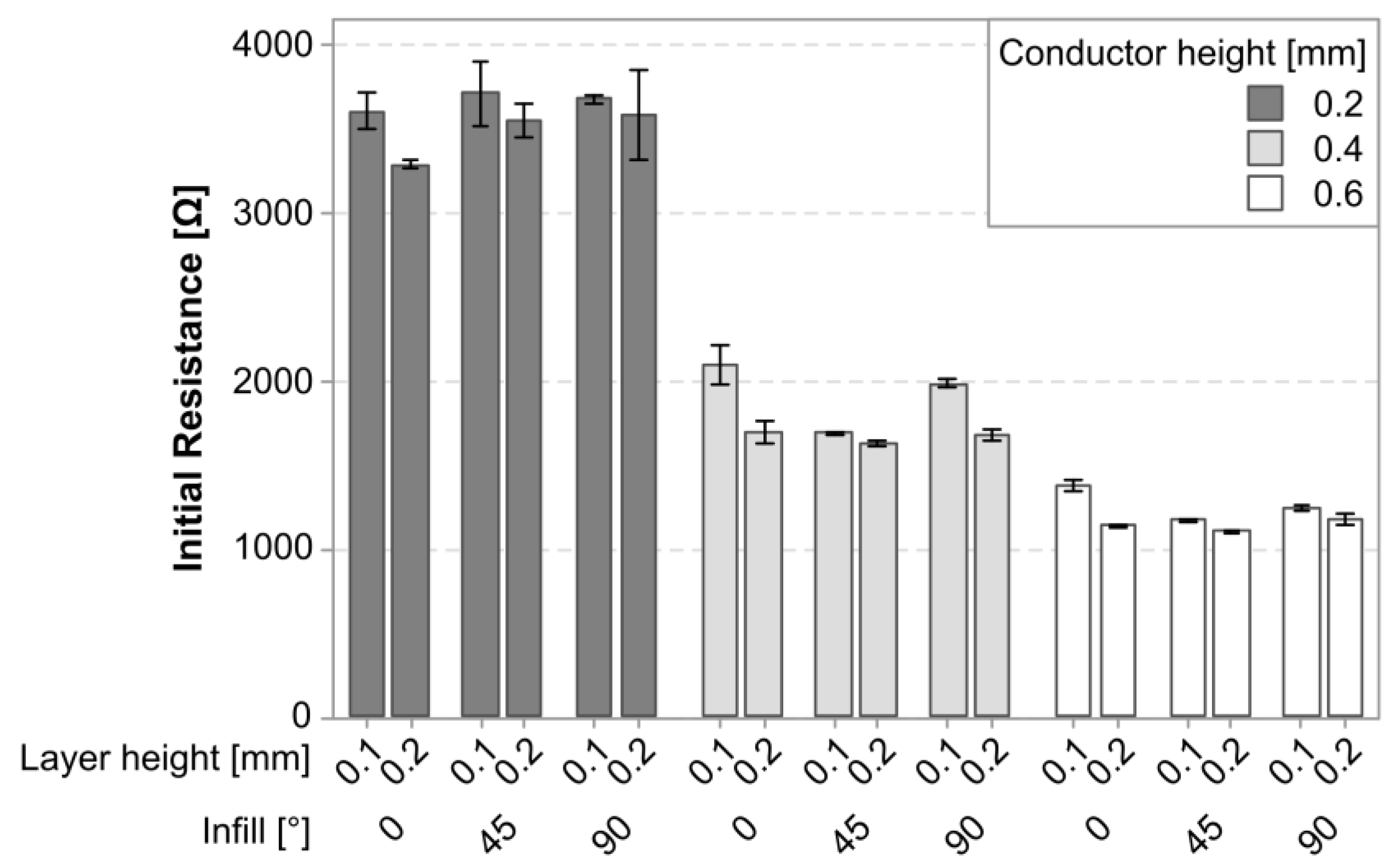
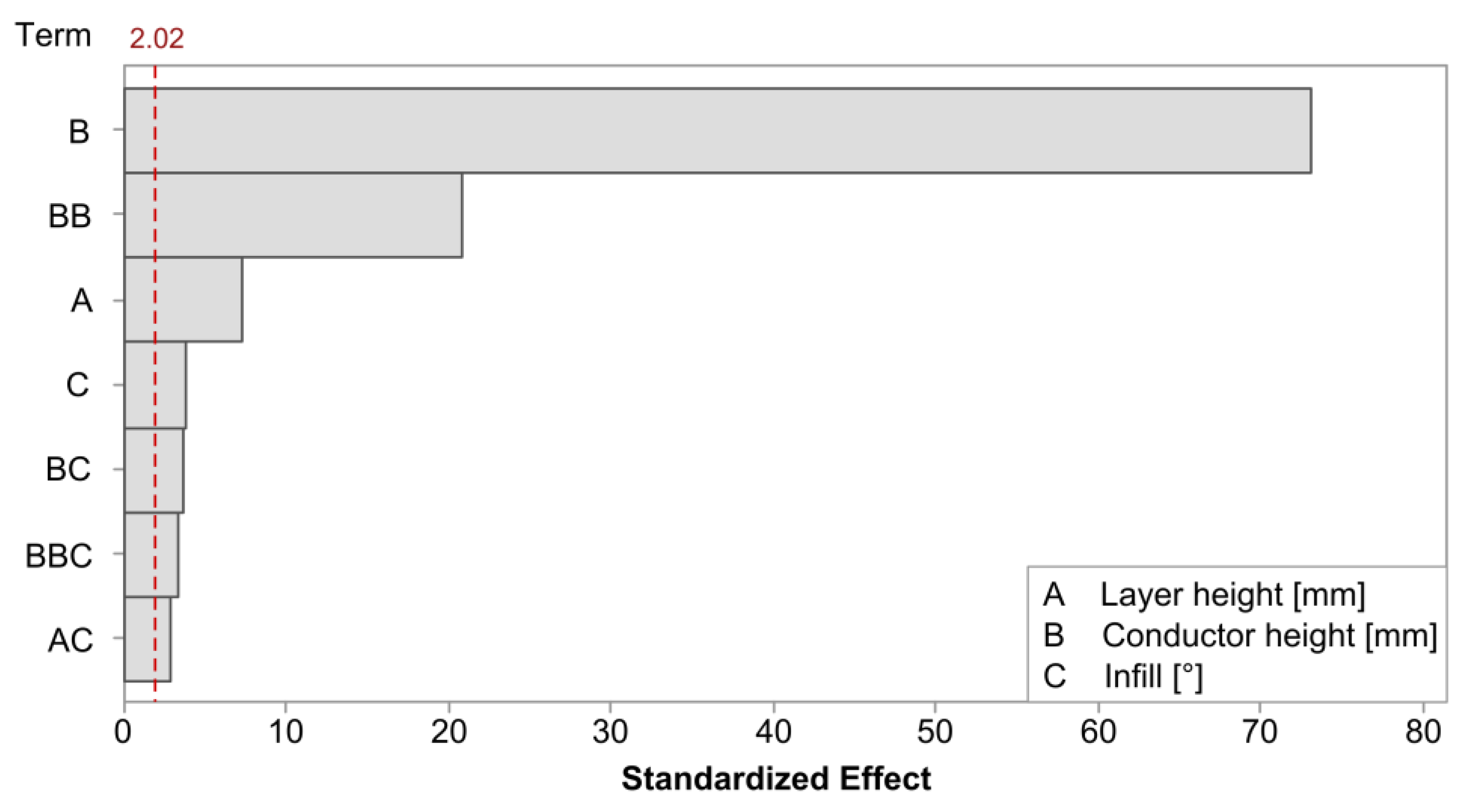
3.1. Initial Resistance
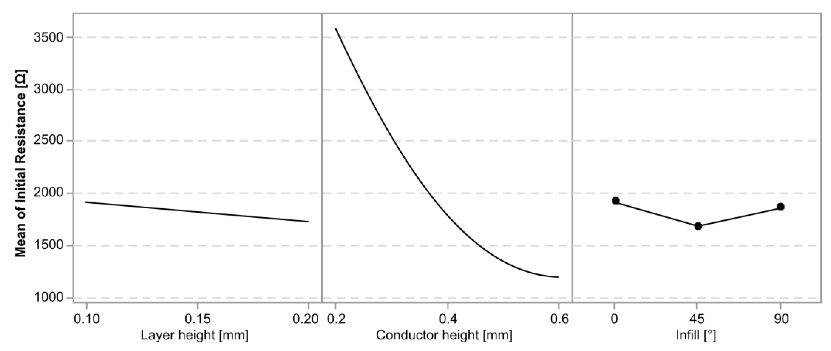
3.1.1. cPLA
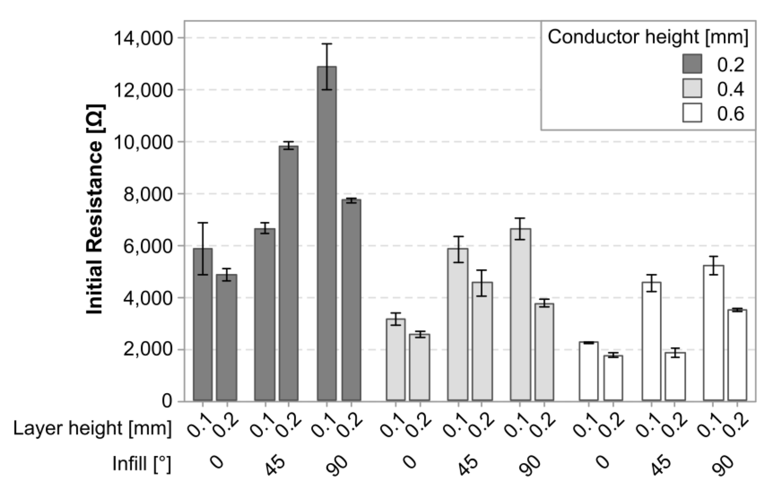
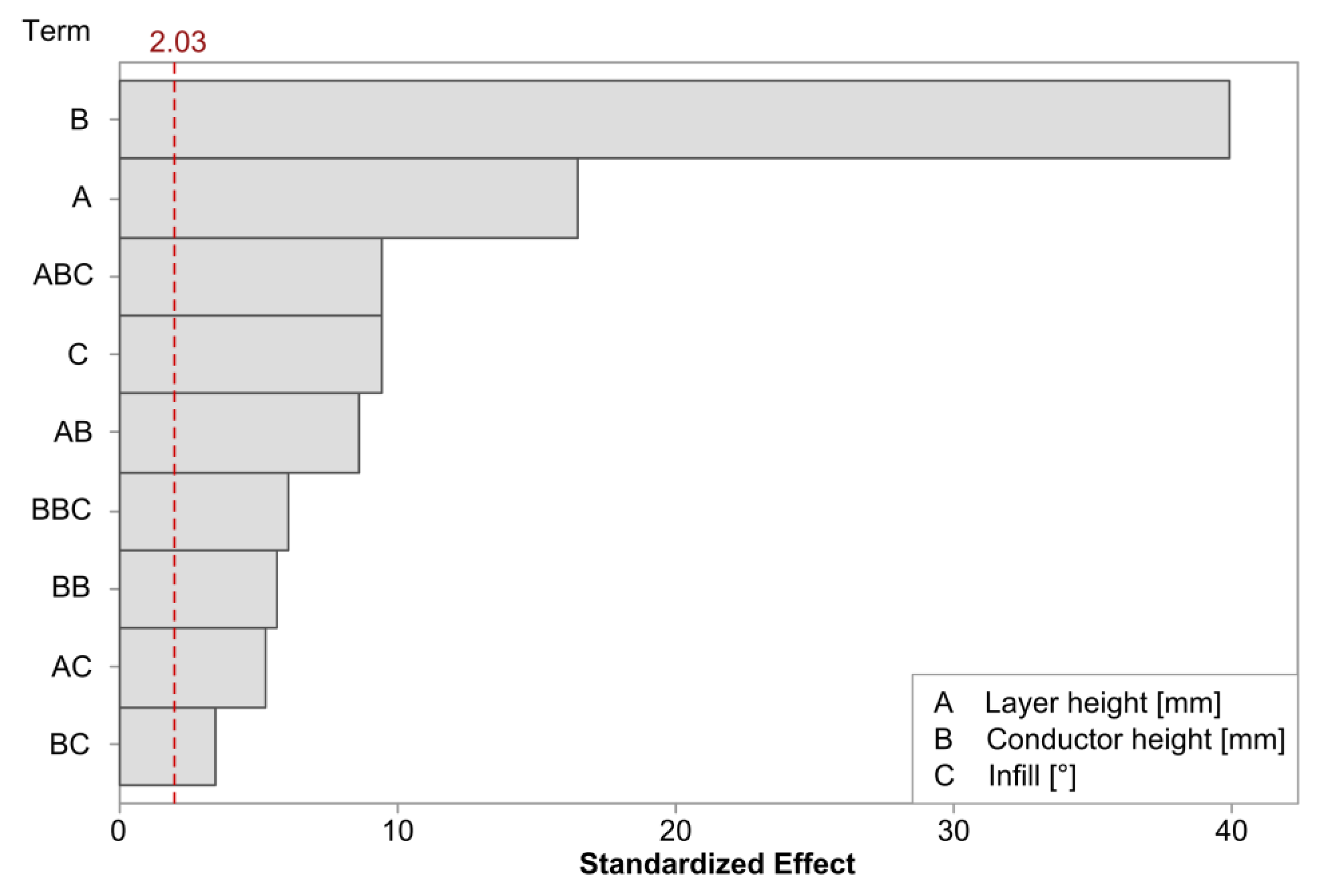
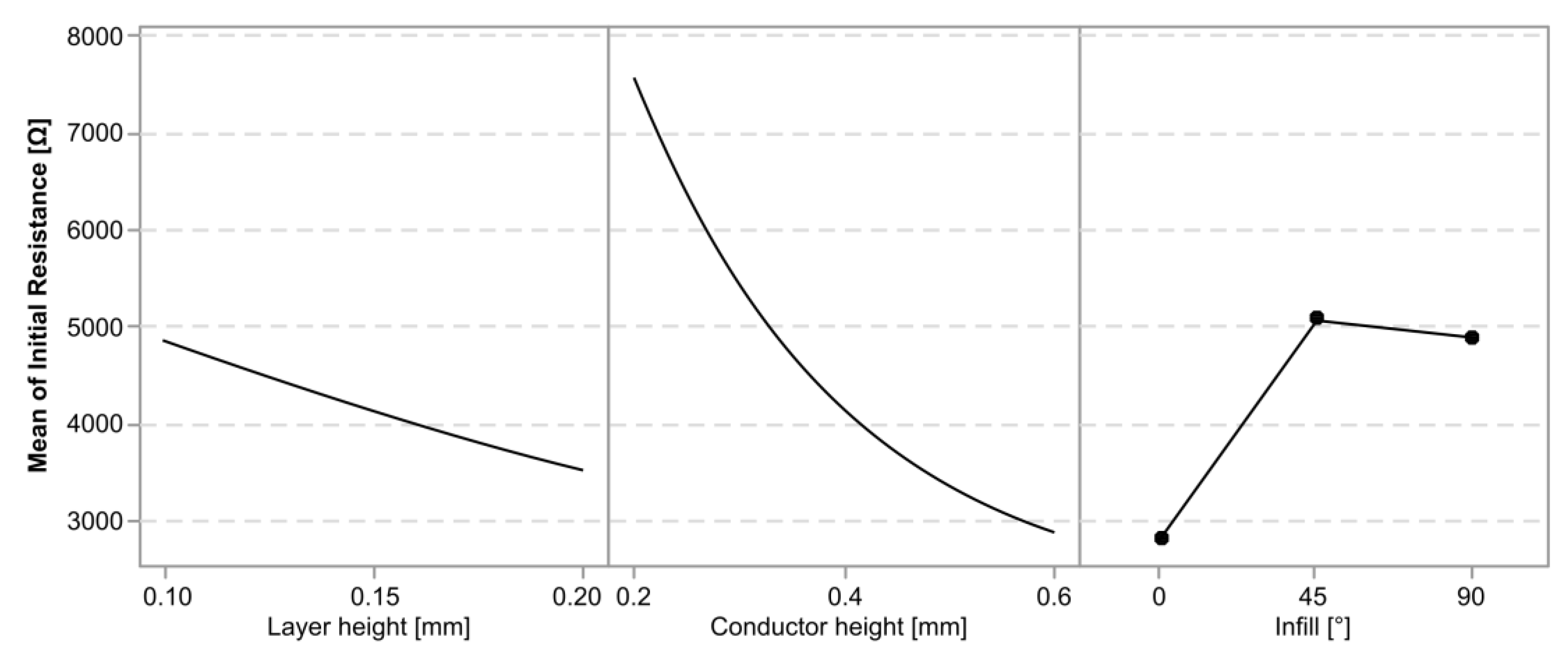
3.1.2. cTPU
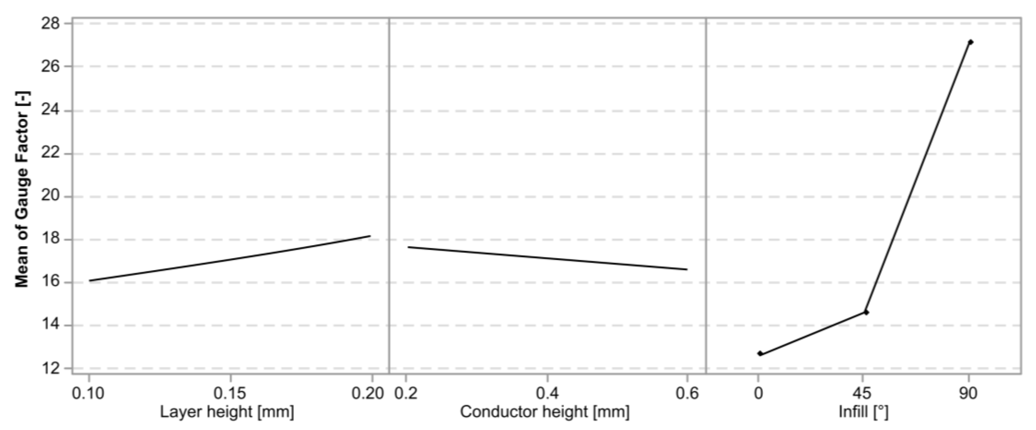
3.2. Gauge Factor
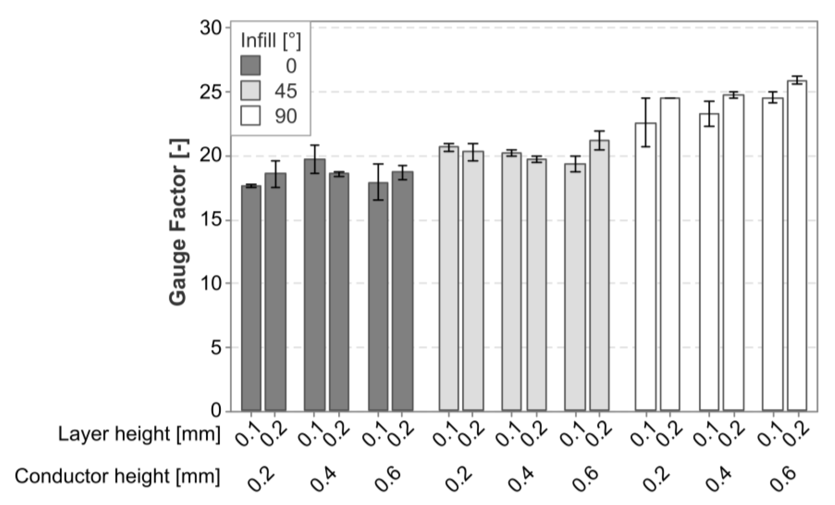
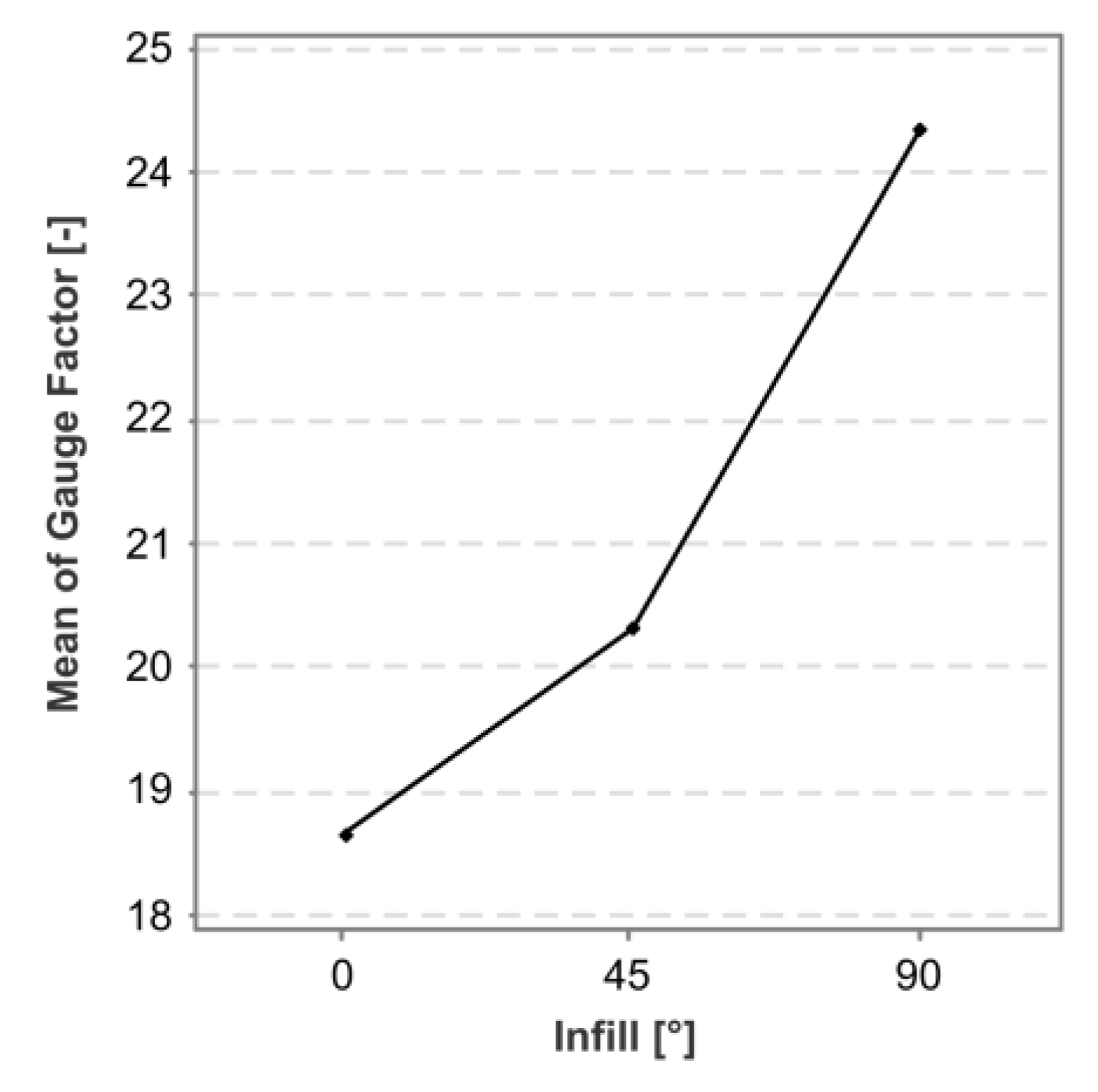
3.2.1. cPLA
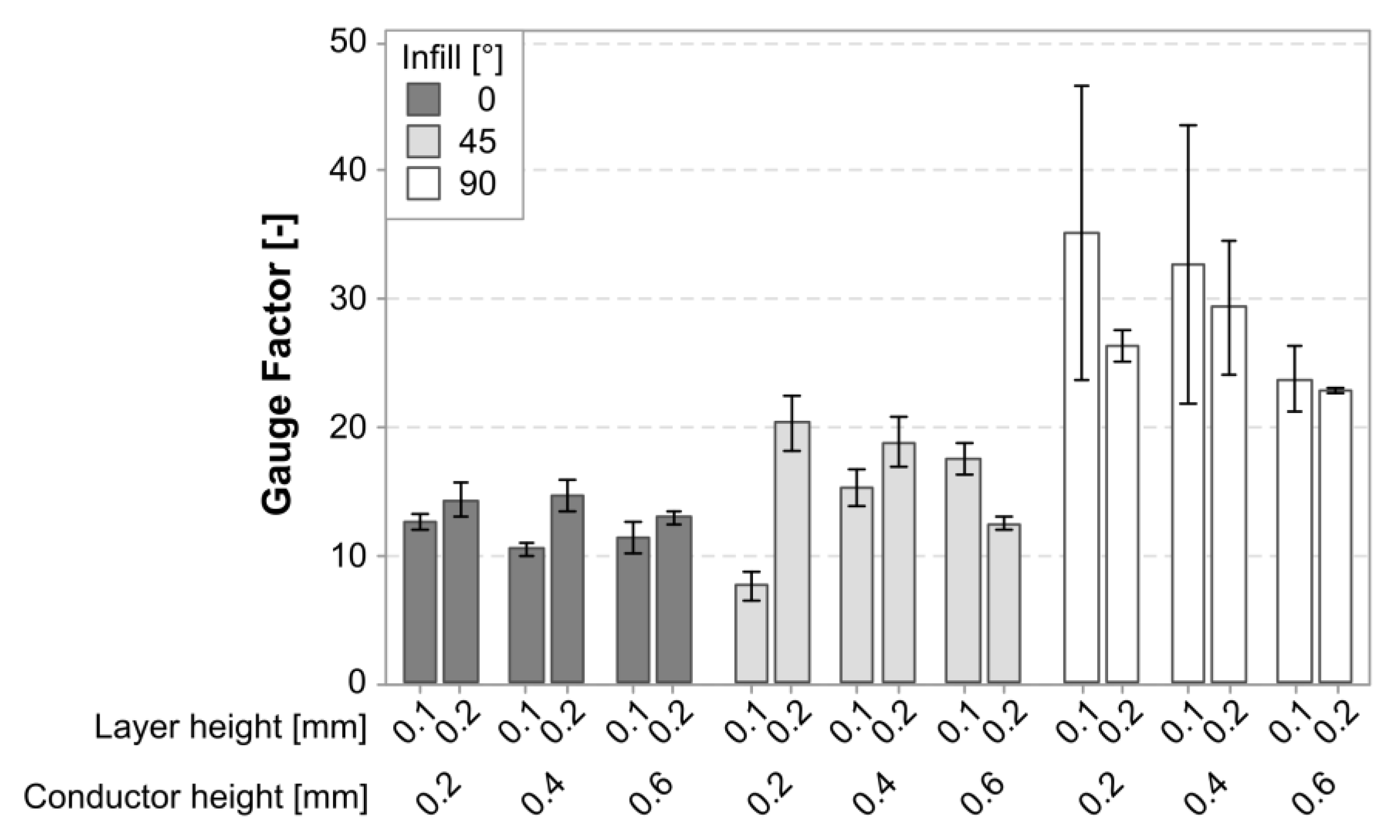
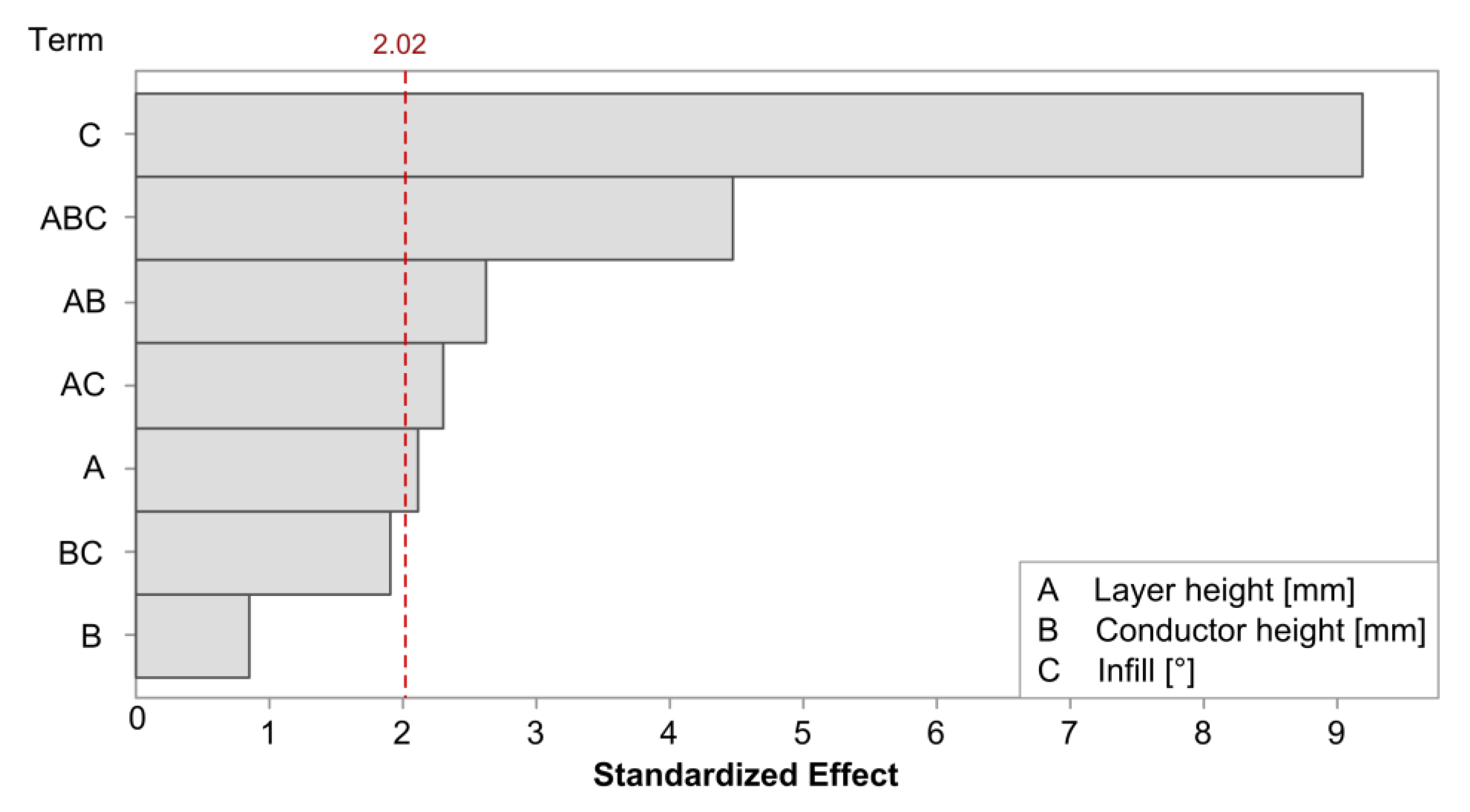
3.2.2. cTPU
4. Discussion
5. Conclusions
Supplementary Materials
Author Contributions
Funding
Data Availability Statement
Acknowledgments
Conflicts of Interest
References
- Gibson, I.; Rosen, D.; Stucker, B. Additive manufacturing technologies. In 3D Printing, Rapid Prototyping, and Direct Digital Manufacturing, 2nd ed.; Gibson, I., Rosen, D., Stucker, B., Eds.; Springer: New York, NY, USA, 2015; ISBN 9781493921133. [Google Scholar]
- Postiglione, G.; Natale, G.; Griffini, G.; Levi, M.; Turri, S. Conductive 3D microstructures by direct 3D printing of polymer/carbon nanotube nanocomposites via liquid deposition modeling. Compos. Part A Appl. Sci. Manuf. 2015, 76, 110–114. [Google Scholar] [CrossRef]
- ISO/ASTM 52900:2015; Additive Manufacturing—General Principles—Terminology. CEN European Committee for Standardization: Brussels, Belgium, 2018.
- Ghabezi, P.; Harrison, N.M.; Flanagan, T. Manufacture of Composite Filament for 3D Printing from Short Glass Fibres and Recycled High-Density Polypropylene. In Proceedings of the 8th World Congress on Mechanical, Chemical, and Material Engineering, Prague, Czech Republic, 31 July–2 August 2022. [Google Scholar]
- Cieślik, M.; Rodak, A.; Susik, A.; Wójcik, N.; Szociński, M.; Ryl, J.; Formela, K. Multiple Reprocessing of Conductive PLA 3D-Printing Filament: Rheology, Morphology, Thermal and Electrochemical Properties Assessment. Materials 2023, 16, 1307. [Google Scholar] [CrossRef] [PubMed]
- Sam-Daliri, O.; Ghabezi, P.; Flanagan, T.; Finnegan, W.; Mitchell, S.; Harrison, N. Recovery of Particle Reinforced Composite 3D Printing Filament from Recycled Industrial Polypropylene and Glass Fibre Waste. In Proceedings of the 8th World Congress on Mechanical, Chemical, and Material Engineering, Prague, Czech Republic, 31 July–2 August 2022. [Google Scholar]
- Leigh, S.J.; Bradley, R.J.; Purssell, C.P.; Billson, D.R.; Hutchins, D.A. A simple, low-cost conductive composite material for 3D printing of electronic sensors. PLoS ONE 2012, 7, e49365. [Google Scholar] [CrossRef] [PubMed]
- Shemelya, C.; Cedillos, F.; Aguilera, E.; Espalin, D.; Muse, D.; Wicker, R.; MacDonald, E. Encapsulated Copper Wire and Copper Mesh Capacitive Sensing for 3-D Printing Applications. IEEE Sens. J. 2015, 15, 1280–1286. [Google Scholar] [CrossRef]
- Agarwala, S.; Goh, G.L.; Yap, Y.L.; Goh, G.D.; Yu, H.; Yeong, W.Y.; Tran, T. Development of bendable strain sensor with embedded microchannels using 3D printing. Sens. Actuators A Phys. 2017, 263, 593–599. [Google Scholar] [CrossRef]
- Angel, K.; Tsang, H.H.; Bedair, S.S.; Smith, G.L.; Lazarus, N. Selective electroplating of 3D printed parts. Addit. Manuf. 2018, 20, 164–172. [Google Scholar] [CrossRef]
- Christ, J.F.; Aliheidari, N.; Ameli, A.; Pötschke, P. 3D printed highly elastic strain sensors of multiwalled carbon nanotube/thermoplastic polyurethane nanocomposites. Mater. Des. 2017, 131, 394–401. [Google Scholar] [CrossRef]
- Christ, J.F.; Aliheidari, N.; Pötschke, P.; Ameli, A. Bidirectional and Stretchable Piezoresistive Sensors Enabled by Multimaterial 3D Printing of Carbon Nanotube/Thermoplastic Polyurethane Nanocomposites. Polymers 2018, 11, 11. [Google Scholar] [CrossRef]
- Xiang, D.; Zhang, X.; Han, Z.; Zhang, Z.; Zhou, Z.; Harkin-Jones, E.; Zhang, J.; Luo, X.; Wang, P.; Zhao, C.; et al. 3D printed high-performance flexible strain sensors based on carbon nanotube and graphene nanoplatelet filled polymer composites. J. Mater. Sci. 2020, 55, 15769–15786. [Google Scholar] [CrossRef]
- Dijkshoorn, A.; Werkman, P.; Welleweerd, M.; Wolterink, G.; Eijking, B.; Delamare, J.; Sanders, R.; Krijnen, G.J.M. Embedded sensing: Integrating sensors in 3-D printed structures. J. Sens. Sens. Syst. 2018, 7, 169–181. [Google Scholar] [CrossRef]
- Watschke, H.; Hilbig, K.; Vietor, T. Design and Characterization of Electrically Conductive Structures Additively Manufactured by Material Extrusion. Appl. Sci. 2019, 9, 779. [Google Scholar] [CrossRef]
- Penumakala, P.K.; Santo, J.; Thomas, A. A critical review on the fused deposition modeling of thermoplastic polymer composites. Compos. Part B Eng. 2020, 201, 108336. [Google Scholar] [CrossRef]
- Mohan, V.B.; Krebs, B.J.; Bhattacharyya, D. Development of novel highly conductive 3D printable hybrid polymer-graphene composites. Mater. Today Commun. 2018, 17, 554–561. [Google Scholar] [CrossRef]
- Schouten, M.; Sanders, R.; Krijnen, G. 3D printed flexible capacitive force sensor with a simple micro-controller based readout. In Proceedings of the 2017 IEEE SENSORS, Glasgow, Scotland, 29 October–1 November 2017; IEEE: Piscataway, NJ, USA, 2017; pp. 1–3, ISBN 978-1-5090-1012-7. [Google Scholar]
- Burch, K.; Doshi, S.; Chaudhari, A.; Thostenson, E.; Higginson, J. Estimating ground reaction force with novel carbon nanotube-based textile insole pressure sensors. Wearable Technol. 2023, 4, e8. [Google Scholar] [CrossRef]
- Stetco, C.; Sam-Daliri, O.; Faller, L.-M.; Zangl, H. Piezocapacitive Sensing for Structural Health Monitoring in Adhesive Joints. In Proceedings of the 2019 IEEE International Instrumentation and Measurement Technology Conference (I2MTC), Auckland, New Zealand, 20–23 May 2019; IEEE: Piscataway, NJ, USA, 2019; pp. 1–5, ISBN 978-1-5386-3460-8. [Google Scholar]
- Ni, Y.; Ji, R.; Long, K.; Bu, T.; Chen, K.; Zhuang, S. A review of 3D-printed sensors. Appl. Spectrosc. Rev. 2017, 52, 623–652. [Google Scholar] [CrossRef]
- Watschke, H.; Goutier, M.; Heubach, J.; Vietor, T.; Leichsenring, K.; Böl, M. Novel Resistive Sensor Design Utilizing the Geometric Freedom of Additive Manufacturing. Appl. Sci. 2021, 11, 113. [Google Scholar] [CrossRef]
- Chung, D.D.L. A critical review of piezoresistivity and its application in electrical-resistance-based strain sensing. J. Mater. Sci. 2020, 55, 15367–15396. [Google Scholar] [CrossRef]
- Xiang, D.; Zhang, X.; Harkin-Jones, E.; Zhu, W.; Zhou, Z.; Shen, Y.; Li, Y.; Zhao, C.; Wang, P. Synergistic effects of hybrid conductive nanofillers on the performance of 3D printed highly elastic strain sensors. Compos. Part A Appl. Sci. Manuf. 2020, 129, 105730. [Google Scholar] [CrossRef]
- Georgopoulou, A.; Vanderborght, B.; Clemens, F. Multi-material 3D Printing of Thermoplastic Elastomers for Development of Soft Robotic Structures with Integrated Sensor Elements. In Industrializing Additive Manufacturing; Meboldt, M., Klahn, C., Eds.; Springer International Publishing: Cham, Switzerland, 2021; pp. 67–81. ISBN 978-3-030-54333-4. [Google Scholar]
- Arh, M.; Slavič, J.; Boltežar, M. Experimental identification of the dynamic piezoresistivity of fused-filament-fabricated structures. Addit. Manuf. 2020, 36, 101493. [Google Scholar] [CrossRef]
- Dul, S.; Pegoretti, A.; Fambri, L. Fused Filament Fabrication of Piezoresistive Carbon Nanotubes Nanocomposites for Strain Monitoring. Front. Mater. 2020, 7, 12. [Google Scholar] [CrossRef]
- Mousavi, S.; Howard, D.; Zhang, F.; Leng, J.; Wang, C.H. Direct 3D Printing of Highly Anisotropic, Flexible, Constriction-Resistive Sensors for Multidirectional Proprioception in Soft Robots. ACS Appl. Mater. Interfaces 2020, 12, 15631–15643. [Google Scholar] [CrossRef] [PubMed]
- Munasinghe, N.; Woods, M.; Miles, G.; Paul, G. 3-D Printed Strain Sensor for Structural Health Monitoring. In Proceedings of the 2019 IEEE International Conference on Cybernetics and Intelligent Systems (CIS) and IEEE Conference on Robotics, Automation and Mechatronics (RAM), Bangkok, Thailand, 18–20 November 2019; pp. 275–280, ISBN 2326-8239. [Google Scholar]
- Kim, K.; Park, J.; Suh, J.-h.; Kim, M.; Jeong, Y.; Park, I. 3D printing of multiaxial force sensors using carbon nanotube (CNT)/thermoplastic polyurethane (TPU) filaments. Sens. Actuators A Phys. 2017, 263, 493–500. [Google Scholar] [CrossRef]
- Hohimer, C.J.; Petrossian, G.; Ameli, A.; Mo, C.; Pötschke, P. 3D printed conductive thermoplastic polyurethane/carbon nanotube composites for capacitive and piezoresistive sensing in soft pneumatic actuators. Addit. Manuf. 2020, 34, 101281. [Google Scholar] [CrossRef]
- Stano, G.; Di Nisio, A.; Lanzolla, A.M.; Ragolia, M.; Percoco, G. Fused filament fabrication of commercial conductive filaments: Experimental study on the process parameters aimed at the minimization, repeatability and thermal characterization of electrical resistance. Int. J. Adv. Manuf. Technol. 2020, 111, 2971–2986. [Google Scholar] [CrossRef]
- Stano, G.; Di Nisio, A.; Lanzolla, A.; Percoco, G. Additive manufacturing and characterization of a load cell with embedded strain gauges. Precis. Eng. 2020, 62, 113–120. [Google Scholar] [CrossRef]
- Maurizi, M.; Slavič, J.; Cianetti, F.; Jerman, M.; Valentinčič, J.; Lebar, A.; Boltežar, M. Dynamic Measurements Using FDM 3D-Printed Embedded Strain Sensors. Sensors 2019, 19, 2661. [Google Scholar] [CrossRef]
- Schouten, M.; Prakken, B.; Sanders, R.; Krijnen, G. Linearisation of a 3D printed flexible tactile sensor based on piezoresistive sensing. In Proceedings of the 2019 IEEE SENSORS, Montreal, QC, Canada, 27–30 October 2019; IEEE: Piscataway, NJ, USA, 2019; pp. 1–4, ISBN 978-1-7281-1634-1. [Google Scholar]
- NinjaTek. Technical Data Sheet—NinjaFlex® 85A by NinjaTek. Available online: https://ninjatek.com/wp-content/uploads/2019/10/NinjaFlex-TDS.pdf (accessed on 3 November 2020).
- NinjaTek. Eel 3D Printing Filament Technical Datasheet. Available online: https://ninjatek.com/wp-content/uploads/Eel-TDS.pdf (accessed on 10 February 2023).
- Proto-Pasta. Proto-Pasta Conductive PLA Technical Data Sheet. Available online: https://cdn.shopify.com/s/files/1/0717/9095/files/TDS__Conductive_PLA_1.0.1.pdf (accessed on 11 April 2023).
- Proto-Pasta. Composite Conductive Fiber PLA Safety Data Sheet. Available online: https://cdn.shopify.com/s/files/1/0717/9095/files/CDP1xxxx_SDS.pdf (accessed on 3 May 2021).
- NinjaTek. EEL 3D Filament Safety Data Sheet. Available online: https://ninjatek.com/wp-content/uploads/SDS_EEL.pdf (accessed on 3 May 2021).
- ISO 20753:2018; Plastics—Test Specimens. CEN European Committee for Standardization: Brussels, Belgium, 2018.
- Hilbig, K.; Nowka, M.; Redeker, J.; Watschke, H.; Friesen, V.; Duden, A.; Vietor, T. Data-Driven Design Support for Additively Manufactured Heating Elements. Proc. Des. Soc. 2022, 2, 1391–1400. [Google Scholar] [CrossRef]
- Schouten, M.; Wolterink, G.; Dijkshoorn, A.; Kosmas, D.; Stramigioli, S.; Krijnen, G. A Review of Extrusion-Based 3D Printing for the Fabrication of Electro-and Biomechanical Sensors. IEEE Sens. J. 2020, 21, 12900–12912. [Google Scholar] [CrossRef]
- Gnanasekaran, K.; Heijmans, T.; van Bennekom, S.; Woldhuis, H.; Wijnia, S.; De With, G.; Friedrich, H. 3D printing of CNT- and graphene-based conductive polymer nanocomposites by fused deposition modeling. Appl. Mater. Today 2017, 9, 21–28. [Google Scholar] [CrossRef]
- ISO 527-1:2019; Plastics—Determination of tensile properties. Part 1: General Principles. CEN European Committee for Standardization: Brussels, Belgium, 2019.
- Regtien, P.P.L. Sensors for Mechatronics; Elsevier: London, UK, 2012; ISBN 9780123944092. [Google Scholar]
- Hampel, B.; Monshausen, S.; Schilling, M. Properties and applications of electrically conductive thermoplastics for additive manufacturing of sensors. Tm-Tech. Mess. 2017, 84, 593–599. [Google Scholar] [CrossRef]
- Dijkshoorn, A.; Schouten, M.; Stramigioli, S.; Krijnen, G. Modelling of Anisotropic Electrical Conduction in Layered Structures 3D-Printed with Fused Deposition Modelling. Sensors 2021, 21, 3710. [Google Scholar] [CrossRef] [PubMed]
- Stano, G.; Ovy, S.M.A.I.; Edwards, J.R.; Cianchetti, M.; Percoco, G.; Tadesse, Y. One-shot additive manufacturing of robotic finger with embedded sensing and actuation. Int. J. Adv. Manuf. Technol. 2023, 124, 467–485. [Google Scholar] [CrossRef]


| Load Case | Material Influences | Process Parameter Influences | Design/Geometry Influences |
|---|---|---|---|
| Tensile load | [11,13,24,25] | [14,26,27,28,29] | [12,28] |
| Compressive load | [7] | [26] | [22] |
| Flexural load | [7,25,30,31] | [31,32,33] | [30,34,35] |
| Abbreviation | Polymer Matrix | Manufacturer | Filament Name | Conductive Filler | Resistivity |
|---|---|---|---|---|---|
| cPLA | Polylactic acid (PLA) | Proto-Pasta | Conductive PLA Filament [38] | Carbon black, ≤21.5% wt. [39] | x/y axis: 30 Ω·cm z axis: 115 Ω·cm |
| cTPU | Thermoplastic polyurethane (TPU) | NinjaTek | Eel 3D Printing Filament [37] | Carbon black, ≤18% wt. [40] | 1.5 × 10³ Ω 1 |
| TPU | Thermoplastic polyurethane (TPU) | NinjaTek | NinjaFlex [36] | None | Non-conductive |
| Variable Name | Experimental Settings |
|---|---|
| Conductive material | cPLA, cTPU |
| Conductor height | 0.2, 0.4, 0.6 mm |
| Layer height | 0.1, 0.2 mm |
| Infill angle | 0°, ±45°, 90° |
| Setting | cPLA | cTPU | TPU |
|---|---|---|---|
| Temperature (°C) | 235 | 235 | 235 |
| Speed (mm/s) | 15 | 20 | 20 |
| Extrusion multiplier (-) | 0.94 | 1.05 | 1.02 |
| Trace width (mm) | 0.4 | 0.4 | 0.4 |
| Shells (-) | 0 | 0 | 2 |
| Sensor Property | Goal | Material | Sensor Height | Layer Height | Infill Angle [°] |
|---|---|---|---|---|---|
| Initial resistance | Minimize | cPLA | Maximize | Maximize | 45 > 0 > 90 |
| cTPU | Maximize | Maximize | 0 > 45 > 90 | ||
| Gauge factor | Maximize | cPLA | Insignificant | Insignificant | 90 > 45 > 0 |
| cTPU | Insignificant | Maximize | 90 > 45 > 0 |
Disclaimer/Publisher’s Note: The statements, opinions and data contained in all publications are solely those of the individual author(s) and contributor(s) and not of MDPI and/or the editor(s). MDPI and/or the editor(s) disclaim responsibility for any injury to people or property resulting from any ideas, methods, instructions or products referred to in the content. |
© 2023 by the authors. Licensee MDPI, Basel, Switzerland. This article is an open access article distributed under the terms and conditions of the Creative Commons Attribution (CC BY) license (https://creativecommons.org/licenses/by/4.0/).
Share and Cite
Goutier, M.; Hilbig, K.; Vietor, T.; Böl, M. Process Parameters and Geometry Effects on Piezoresistivity in Additively Manufactured Polymer Sensors. Polymers 2023, 15, 2159. https://doi.org/10.3390/polym15092159
Goutier M, Hilbig K, Vietor T, Böl M. Process Parameters and Geometry Effects on Piezoresistivity in Additively Manufactured Polymer Sensors. Polymers. 2023; 15(9):2159. https://doi.org/10.3390/polym15092159
Chicago/Turabian StyleGoutier, Marijn, Karl Hilbig, Thomas Vietor, and Markus Böl. 2023. "Process Parameters and Geometry Effects on Piezoresistivity in Additively Manufactured Polymer Sensors" Polymers 15, no. 9: 2159. https://doi.org/10.3390/polym15092159
APA StyleGoutier, M., Hilbig, K., Vietor, T., & Böl, M. (2023). Process Parameters and Geometry Effects on Piezoresistivity in Additively Manufactured Polymer Sensors. Polymers, 15(9), 2159. https://doi.org/10.3390/polym15092159