
Defect Passivation Scheme toward High-Performance Halide Perovskite Solar Cells


Abstract
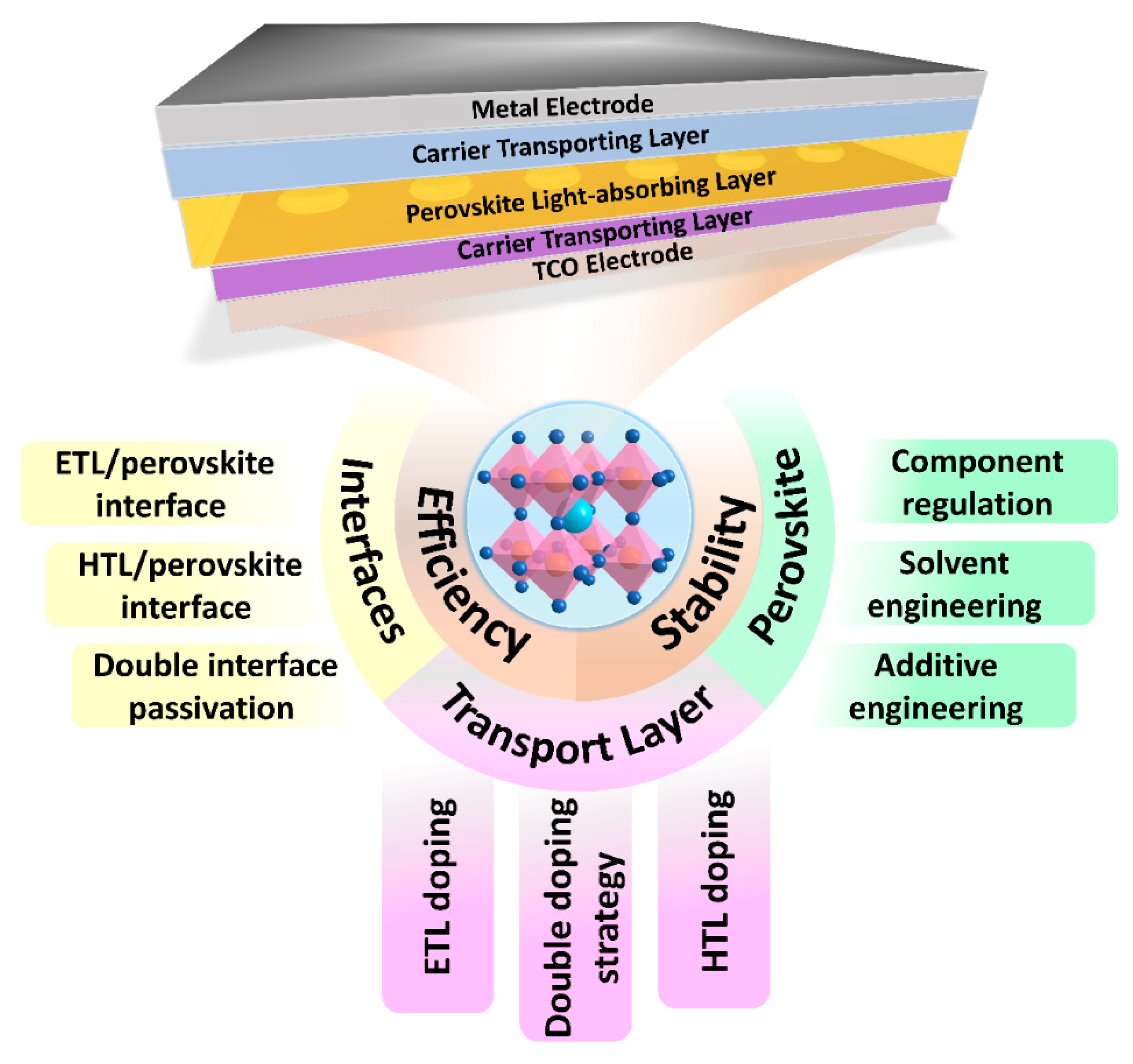
1. Introduction
2. Interface Engineering
2.1. ETL/Perovskite Interface Passivation
2.2. HTL/Perovskite Interface Passivation
3. Perovskite Surface Treatment
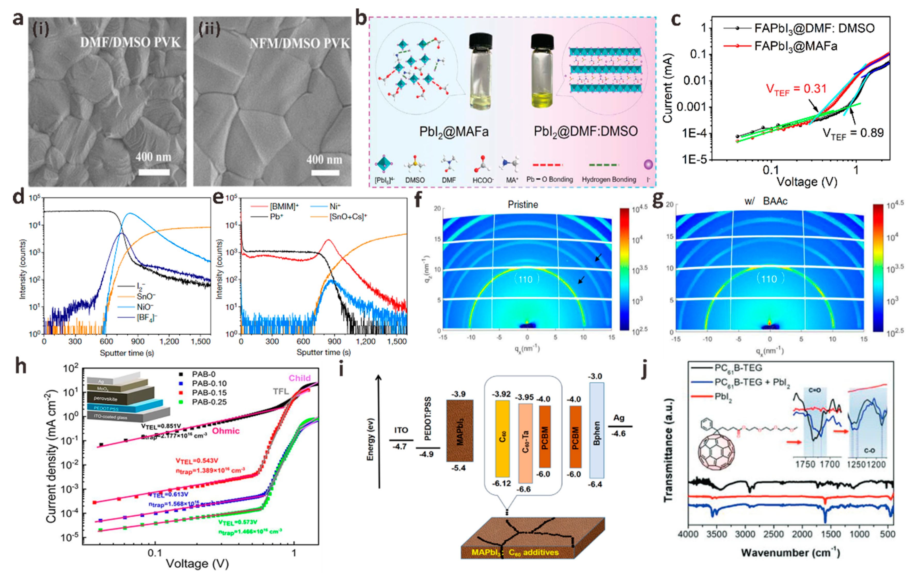
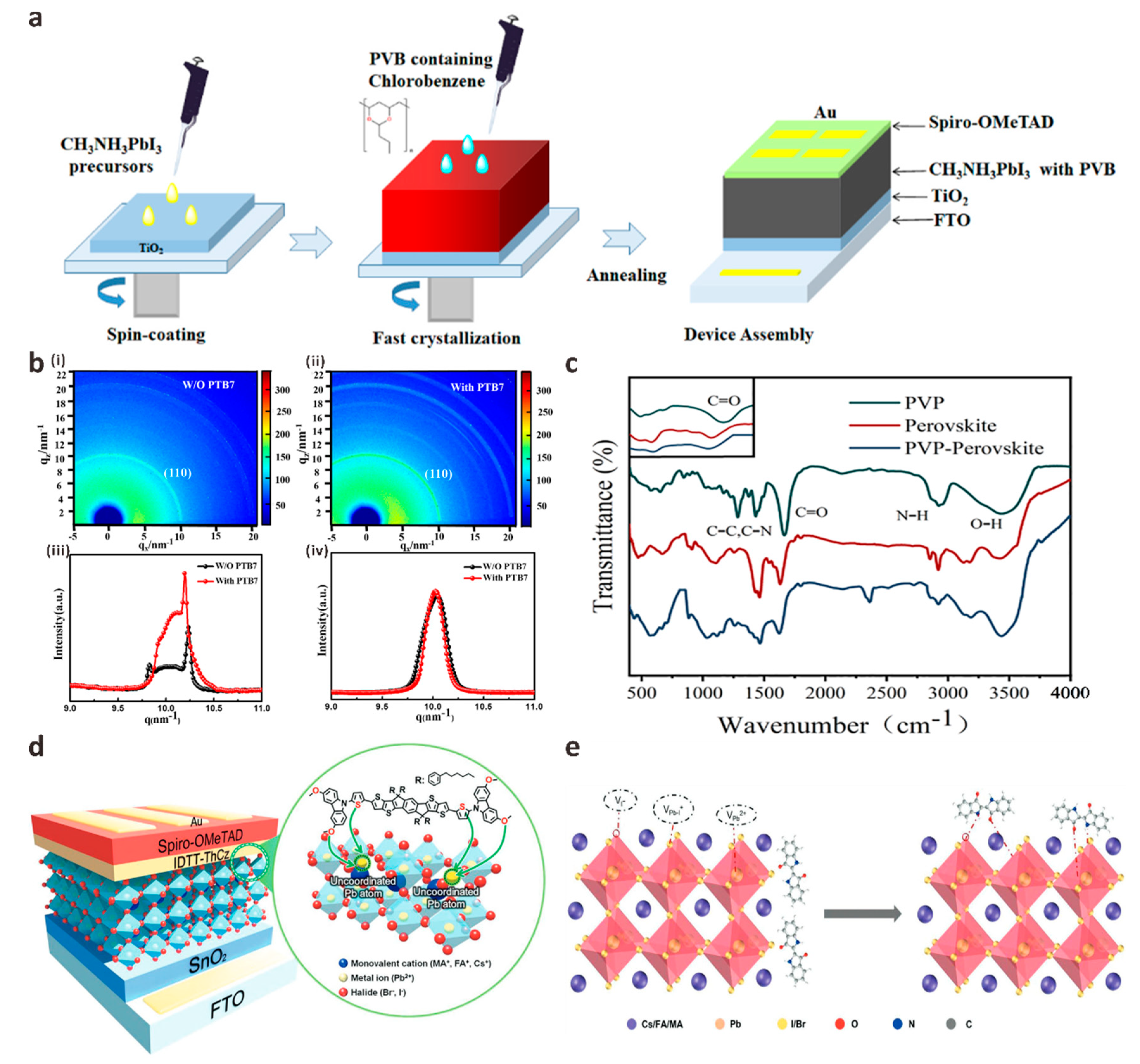
3.1. The Solvent Component
3.2. Precursor Additive Engineering
3.3. Anti-Solvent Engineering
4. Dopant Passivation
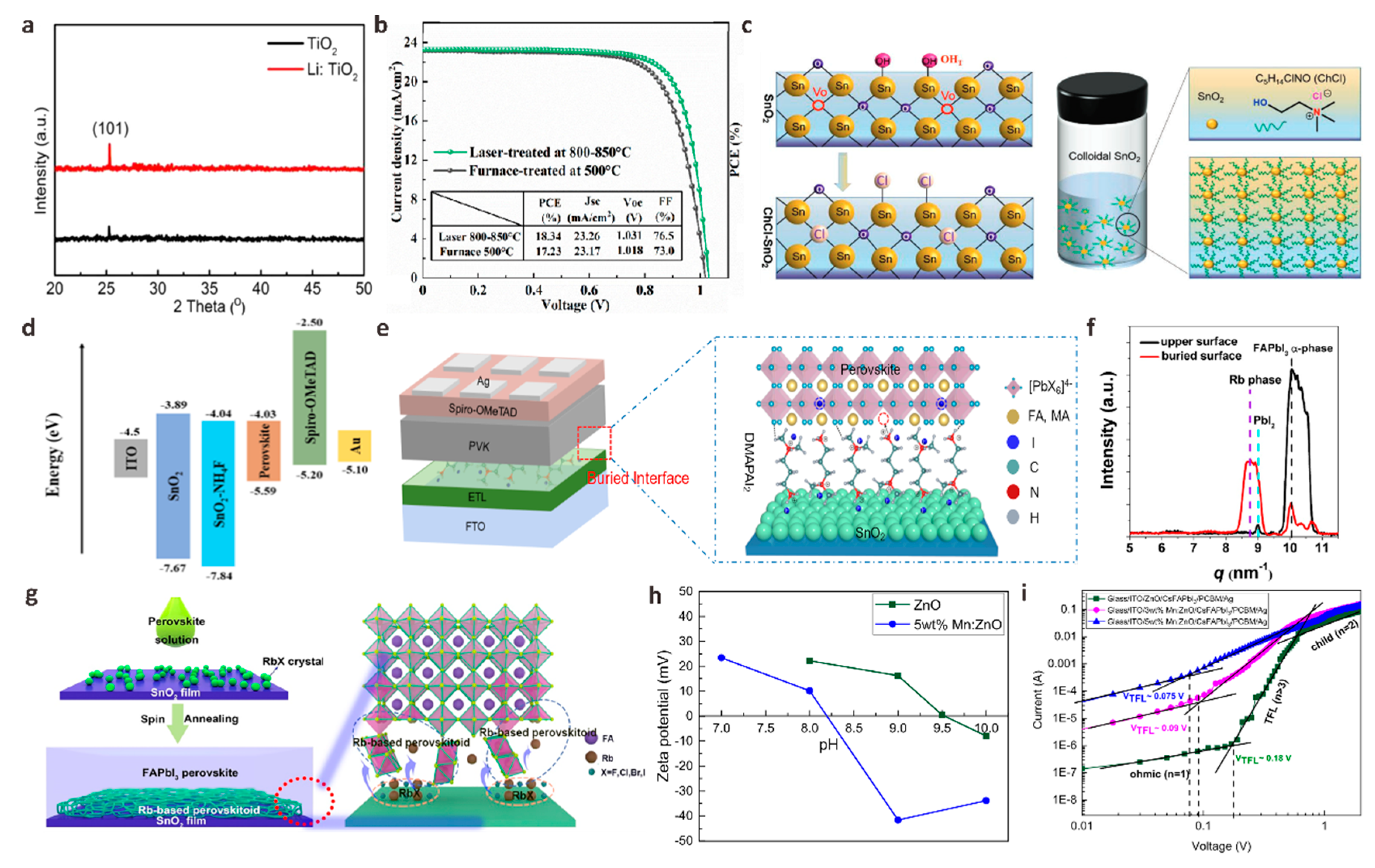
4.1. ETL Doping
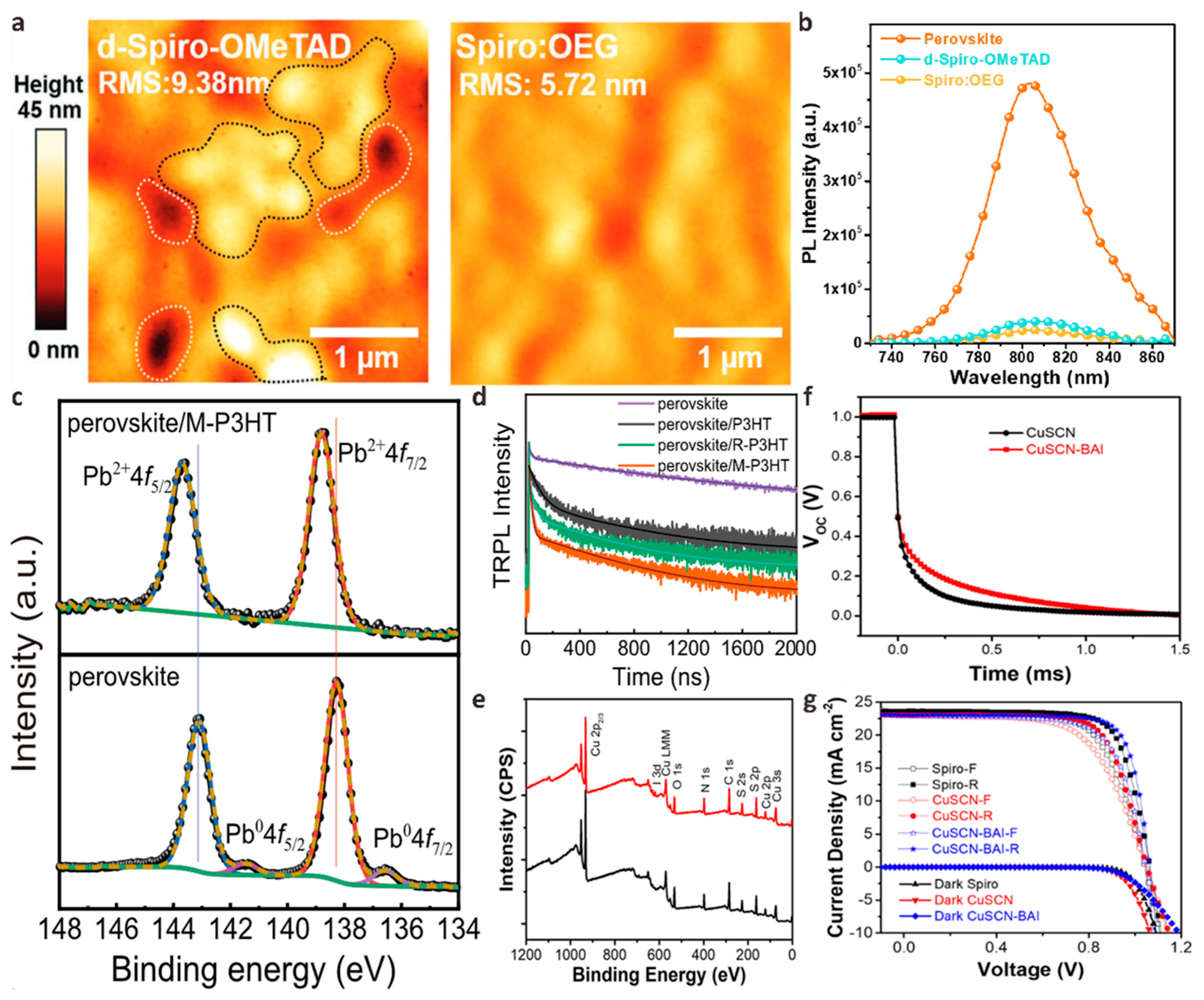
4.2. HTL Doping
5. Summary and Prospect
Author Contributions
Funding
Institutional Review Board Statement
Informed Consent Statement
Data Availability Statement
Conflicts of Interest
References
- Xiang, H.; Liu, P.; Wang, W.; Ran, R.; Zhou, W.; Shao, Z. Towards highly stable and efficient planar perovskite solar cells: Materials development, defect control and interfacial engineering. Chem. Eng. J. 2021, 420, 127599. [Google Scholar] [CrossRef]
- Kim, D.H.; Whitaker, J.B.; Li, Z.; van Hest, M.F.A.M.; Zhu, K. Outlook and Challenges of Perovskite Solar Cells toward Terawatt-Scale Photovoltaic Module Technology. Joule 2018, 2, 1437–1451. [Google Scholar] [CrossRef]
- Roy, P.; Kumar Sinha, N.; Tiwari, S.; Khare, A. A review on perovskite solar cells: Evolution of architecture, fabrication techniques, commercialization issues and status. Sol. Energy 2020, 198, 665–688. [Google Scholar] [CrossRef]
- Chapin, D.M.; Fuller, C.S.; Pearson, G.L. A New Silicon p-n Junction Photocell for Converting Solar Radiation into Electrical Power. J. Appl. Phys. 1954, 25, 676–677. [Google Scholar] [CrossRef]
- Green, M.A.; Dunlop, E.D.; Hohl-Ebinger, J.; Siefer, G.; Yoshita, M.; Kopidakis, N.; Bothe, K.; Hao, X. Solar cell efficiency tables (version 61). Prog. Photovolt. 2023, 31, 3–16. [Google Scholar] [CrossRef]
- Yoshikawa, K.; Kawasaki, H.; Yoshida, W.; Irie, T.; Konishi, K.; Nakano, K.; Uto, T.; Adachi, D.; Kanematsu, M.; Uzu, H.; et al. Silicon heterojunction solar cell with interdigitated back contacts for a photoconversion efficiency over 26%. Nat. Energy 2017, 2, 17032. [Google Scholar] [CrossRef]
- Liu, W.; Li, H.; Qiao, B.; Zhao, S.; Xu, Z.; Song, D. Highly efficient CIGS solar cells based on a new CIGS bandgap gradient design characterized by numerical simulation. Sol. Energy 2022, 233, 337–344. [Google Scholar] [CrossRef]
- NREL Efficiency Chart. Available online: https://www.nrel.gov/pv/cell-efficiency.html (accessed on 10 November 2022).
- Wu, P.; Wang, S.; Li, X.; Zhang, F. Advances in SnO2-based perovskite solar cells: From preparation to photovoltaic applications. J. Mater. Chem. A 2021, 9, 19554–19588. [Google Scholar] [CrossRef]
- Huang, J.; Yuan, Y.; Shao, Y.; Yan, Y. Understanding the physical properties of hybrid perovskites for photovoltaic applications. Nat. Rev. Mater. 2017, 2, 17042. [Google Scholar] [CrossRef]
- Huang, J.; Shao, Y.; Dong, Q. Organometal Trihalide Perovskite Single Crystals: A Next Wave of Materials for 25% Efficiency Photovoltaics and Applications Beyond? J. Phys. Chem. Lett. 2015, 6, 3218–3227. [Google Scholar] [CrossRef]
- Bush, K.A.; Palmstrom, A.F.; Yu, Z.J.; Boccard, M.; Cheacharoen, R.; Mailoa, J.P.; McMeekin, D.P.; Hoye, R.L.Z.; Bailie, C.D.; Leijtens, T.; et al. 23.6%-efficient monolithic perovskite/silicon tandem solar cells with improved stability. Nat. Energy 2017, 2, 17009. [Google Scholar] [CrossRef]
- Sahli, F.; Werner, J.; Kamino, B.A.; Brauninger, M.; Monnard, R.; Paviet-Salomon, B.; Barraud, L.; Ding, L.; Diaz Leon, J.J.; Sacchetto, D.; et al. Fully textured monolithic perovskite/silicon tandem solar cells with 25.2% power conversion efficiency. Nat. Mater. 2018, 17, 820–826. [Google Scholar] [CrossRef] [PubMed]
- Kojima, A.; Teshima, K.; Shirai, Y.; Miyasaka, T. Organometal Halide Perovskites as Visible-Light Sensitizers for Photovoltaic Cells. J. Am. Chem. Soc. 2009, 131, 6050–6051. [Google Scholar] [CrossRef] [PubMed]
- Kim, H.S.; Lee, C.R.; Im, J.H.; Lee, K.B.; Moehl, T.; Marchioro, A.; Moon, S.J.; Humphry-Baker, R.; Yum, J.H.; Moser, J.E.; et al. Lead iodide perovskite sensitized all-solid-state submicron thin film mesoscopic solar cell with efficiency exceeding 9%. Sci. Rep. 2012, 2, 591. [Google Scholar] [CrossRef] [PubMed]
- Min, H.; Kim, M.; Lee, S.-U.; Kim, H.; Kim, G.; Choi, K.; Lee, J.H.; Seok, S.I. Efficient, stable solar cells by using inherent bandgap of alpha-phase formamidinium lead iodide. Science 2019, 366, 749–753. [Google Scholar] [CrossRef]
- Jeong, M.; Choi, I.W.; Go, E.M.; Cho, Y.; Kim, M.; Lee, B.; Jeong, S.; Jo, Y.; Choi, H.W.; Lee, J.; et al. Stable perovskite solar cells with efficiency exceeding 24.8% and 0.3-V voltage loss. Science 2020, 369, 1615–1620. [Google Scholar] [CrossRef]
- Yoo, J.J.; Seo, G.; Chua, M.R.; Park, T.G.; Lu, Y.; Rotermund, F.; Kim, Y.K.; Moon, C.S.; Jeon, N.J.; Correa-Baena, J.P.; et al. Efficient perovskite solar cells via improved carrier management. Nature 2021, 590, 587–593. [Google Scholar] [CrossRef] [PubMed]
- Min, H.; Lee, D.Y.; Kim, J.; Kim, G.; Lee, K.S.; Kim, J.; Paik, M.J.; Kim, Y.K.; Kim, K.S.; Kim, M.G.; et al. Perovskite solar cells with atomically coherent interlayers on SnO2 electrodes. Nature 2021, 598, 444–450. [Google Scholar] [CrossRef]
- Zhao, Y.; Ma, F.; Qu, Z.; Yu, S.; Shen, T.; Deng, H.-X.; Chu, X.; Peng, X.; Yuan, Y.; Zhang, X.; et al. Inactive (PbI2)2 RbCl stabilizes perovskite films for efficient solar cells. Science 2022, 377, 531–534. [Google Scholar] [CrossRef]
- Tan, S.; Huang, T.; Yavuz, I.; Wang, R.; Yoon, T.W.; Xu, M.; Xing, Q.; Park, K.; Lee, D.K.; Chen, C.H.; et al. Stability-limiting heterointerfaces of perovskite photovoltaics. Nature 2022, 605, 268–273. [Google Scholar] [CrossRef]
- Chen, B.; Rudd, P.N.; Yang, S.; Yuan, Y.; Huang, J. Imperfections and their passivation in halide perovskite solar cells. Chem. Soc. Rev. 2019, 48, 3842–3867. [Google Scholar] [CrossRef]
- Shockley, W.; Read, W.T. Statistics of the Recombinations of Holes and Electrons. Phys. Rev. 1952, 87, 835–842. [Google Scholar] [CrossRef]
- Ono, L.K.; Liu, S.F.; Qi, Y. Reducing Detrimental Defects for High-Performance Metal Halide Perovskite Solar Cells. Angew. Chem. Int. Ed. 2020, 59, 6676–6698. [Google Scholar] [CrossRef] [PubMed]
- Chen, J.; Park, N.G. Causes and Solutions of Recombination in Perovskite Solar Cells. Adv. Mater. 2019, 31, 1803019. [Google Scholar] [CrossRef] [PubMed]
- Park, K.; Lee, J.-H.; Lee, J.-W. Surface Defect Engineering of Metal Halide Perovskites for Photovoltaic Applications. ACS Energy Lett. 2022, 7, 1230–1239. [Google Scholar] [CrossRef]
- Schulz, P.; Cahen, D.; Kahn, A. Halide Perovskites: Is It All about the Interfaces? Chem. Rev. 2019, 119, 3349–3417. [Google Scholar] [CrossRef]
- Ni, Z.; Bao, C.; Liu, Y.; Jiang, Q.; Wu, W.-Q.; Chen, S.; Dai, X.; Chen, B.; Hartweg, B.; Yu, Z.; et al. Resolving spatial and energetic distributions of trap states in metal halide perovskite solar cells. Science 2020, 367, 1352–1358. [Google Scholar] [CrossRef] [PubMed]
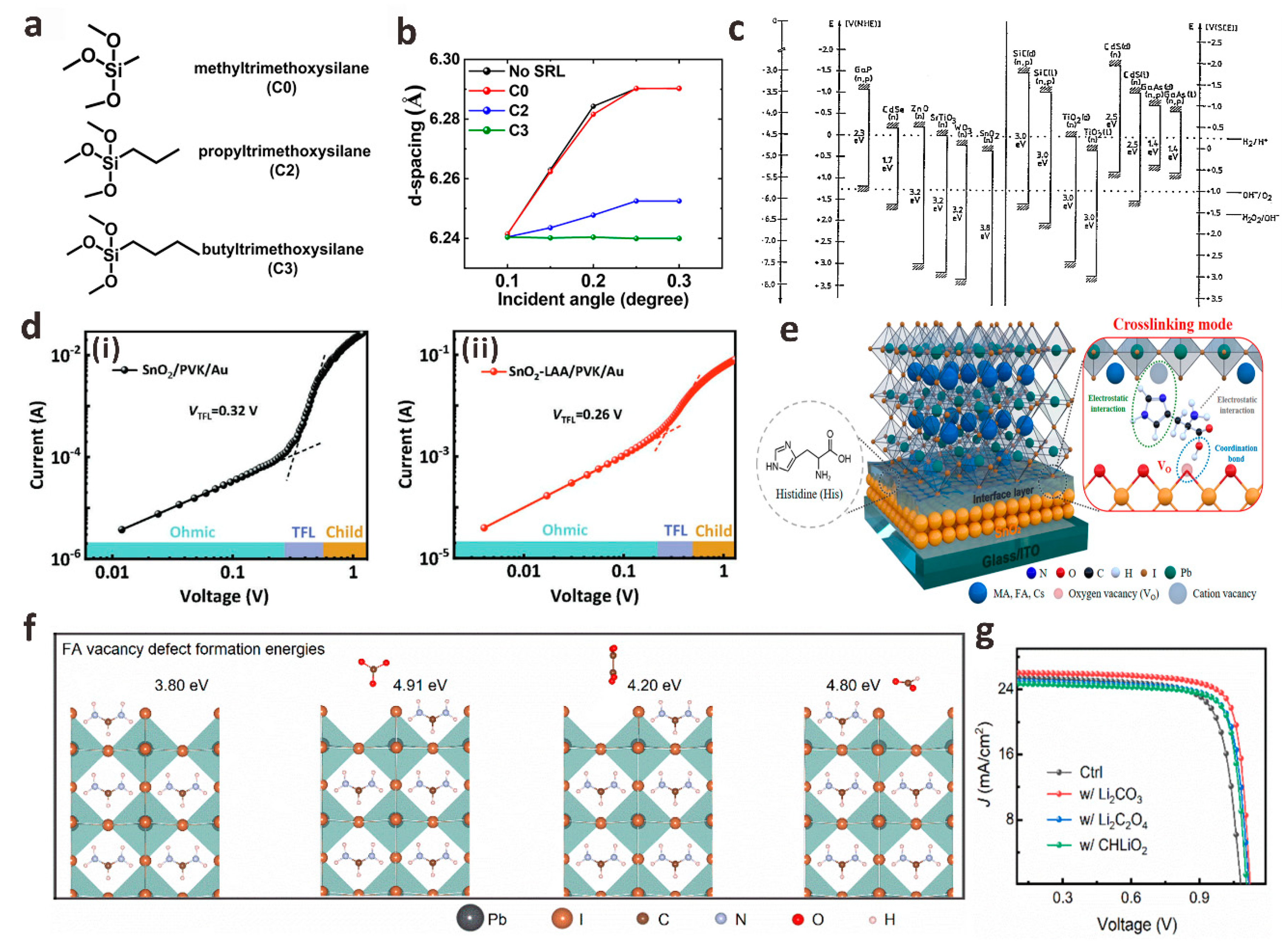
- Liu, T.; Zhao, X.; Zhong, X.; Burlingame, Q.C.; Kahn, A.; Loo, Y.-L. Improved Absorber Phase Stability, Performance, and Lifetime in Inorganic Perovskite Solar Cells with Alkyltrimethoxysilane Strain-Release Layers at the Perovskite/TiO2 Interface. ACS Energy Lett. 2022, 7, 3531–3538. [Google Scholar] [CrossRef]
- Wei, Y.; Rong, B.; Chen, X.; Chen, Y.; Liu, H.; Ye, X.; Huang, Y.; Fan, L.; Wu, J. Efficiency improvement of perovskite solar cell utilizing cystamine dihydrochloride for interface modification. Mater. Res. Bull. 2022, 155, 111949. [Google Scholar] [CrossRef]
- Nozik, A.J.; Memming, R. Physical Chemistry of Semiconductor−Liquid Interfaces. J. Phys. Chem. 1996, 100, 13061–13078. [Google Scholar] [CrossRef]
- Geng, Q.; Jia, X.; He, Z.; Hu, Y.; Gao, Y.; Yang, S.; Yao, C.; Zhang, S. Interface Engineering via Amino Acid for Efficient and Stable Perovskite Solar Cells. Adv. Mater. Interfaces 2022, 9, 2201641. [Google Scholar] [CrossRef]
- Li, Y.; Li, S.; Shen, Y.; Han, X.; Li, Y.; Yu, Y.; Huang, M.; Tao, X. Multifunctional Histidine Cross-Linked Interface toward Efficient Planar Perovskite Solar Cells. ACS Appl. Mater. Interfaces 2022, 14, 47872–47881. [Google Scholar] [CrossRef] [PubMed]
- Zhang, Y.; Kong, T.; Xie, H.; Song, J.; Li, Y.; Ai, Y.; Han, Y.; Bi, D. Molecularly Tailored SnO2/Perovskite Interface Enabling Efficient and Stable FAPbI3 Solar Cells. ACS Energy Lett. 2022, 7, 929–938. [Google Scholar] [CrossRef]
- Jiang, Q.; Zhang, X.; You, J. SnO2: A Wonderful Electron Transport Layer for Perovskite Solar Cells. Small 2018, 14, 1801154. [Google Scholar] [CrossRef]
- Park, S.Y.; Zhu, K. Advances in SnO2 for Efficient and Stable n-i-p Perovskite Solar Cells. Adv. Mater. 2022, 34, 2110438. [Google Scholar] [CrossRef] [PubMed]
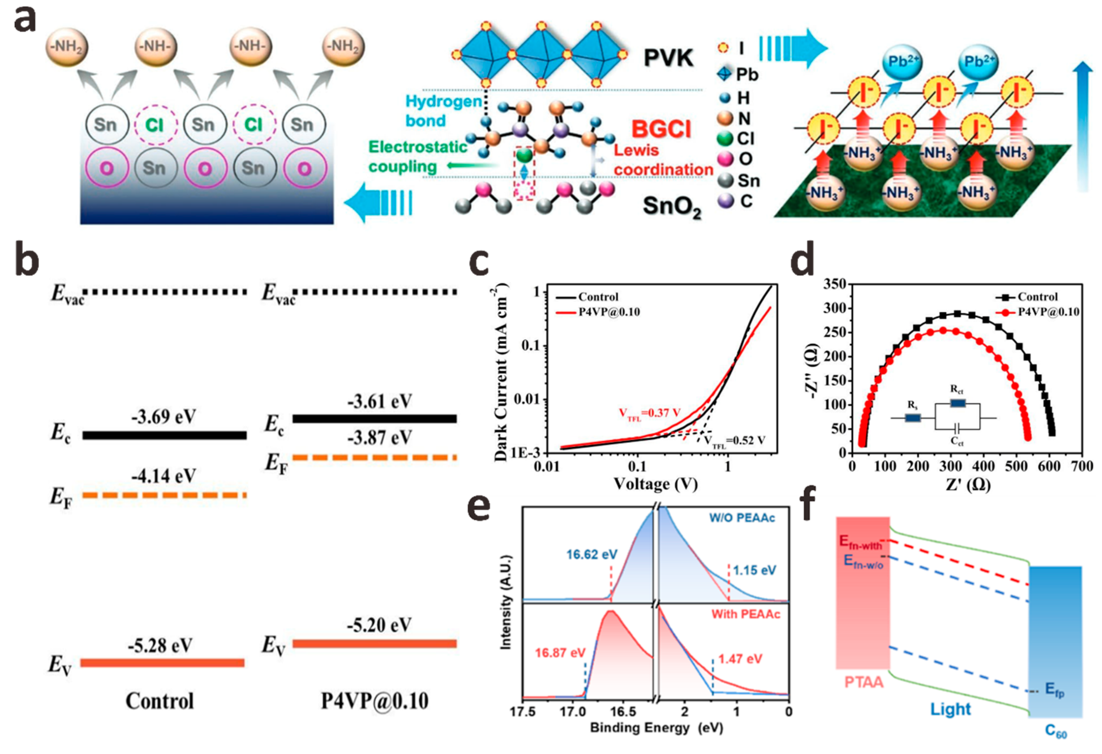
- Zhuang, Q.; Zhang, C.; Gong, C.; Li, H.; Li, H.; Zhang, Z.; Yang, H.; Chen, J.; Zang, Z. Tailoring multifunctional anion modifiers to modulate interfacial chemical interactions for efficient and stable perovskite solar cells. Nano Energy 2022, 102, 107747. [Google Scholar] [CrossRef]
- Xiong, Z.; Chen, X.; Zhang, B.; Odunmbaku, G.O.; Ou, Z.; Guo, B.; Yang, K.; Kan, Z.; Lu, S.; Chen, S.; et al. Simultaneous Interfacial Modification and Crystallization Control by Biguanide Hydrochloride for Stable Perovskite Solar Cells with PCE of 24.4%. Adv. Mater. 2022, 34, 2106118. [Google Scholar] [CrossRef]
- Zhang, Q.; Xiong, S.; Ali, J.; Qian, K.; Li, Y.; Feng, W.; Hu, H.; Song, J.; Liu, F. Polymer interface engineering enabling high-performance perovskite solar cells with improved fill factors of over 82%. J. Mater. Chem. C 2020, 8, 5467–5475. [Google Scholar] [CrossRef]
- Chen, J.; Wang, D.; Chen, S.; Hu, H.; Li, Y.; Huang, Y.; Zhang, Z.; Jiang, Z.; Xu, J.; Sun, X.; et al. Dually Modified Wide-Bandgap Perovskites by Phenylethylammonium Acetate toward Highly Efficient Solar Cells with Low Photovoltage Loss. ACS Appl. Mater. Interfaces 2022, 14, 43246–43256. [Google Scholar] [CrossRef]
- Wan, F.; Ke, L.; Yuan, Y.; Ding, L. Passivation with crosslinkable diamine yields 0.1 V non-radiative Voc loss in inverted perovskite solar cells. Sci. Bull. 2021, 66, 417–420. [Google Scholar] [CrossRef]
- Kamat, P.V. Evolution of Perovskite Photovoltaics and Decrease in Energy Payback Time. J. Phys. Chem. Lett. 2013, 4, 3733–3734. [Google Scholar] [CrossRef]
- Wang, H.; Ye, F.; Liang, J.; Liu, Y.; Hu, X.; Zhou, S.; Chen, C.; Ke, W.; Tao, C.; Fang, G. Pre-annealing treatment for high-efficiency perovskite solar cells via sequential deposition. Joule 2022, 6, 2869–2884. [Google Scholar] [CrossRef]
- Cai, W.; Wang, Y.; Shang, W.; Liu, J.; Wang, M.; Dong, Q.; Han, Y.; Li, W.; Ma, H.; Wang, P.; et al. Lewis base governing superfacial proton behavior of hybrid perovskite: Basicity dependent passivation strategy. Chem. Eng. J. 2022, 446, 137033. [Google Scholar] [CrossRef]
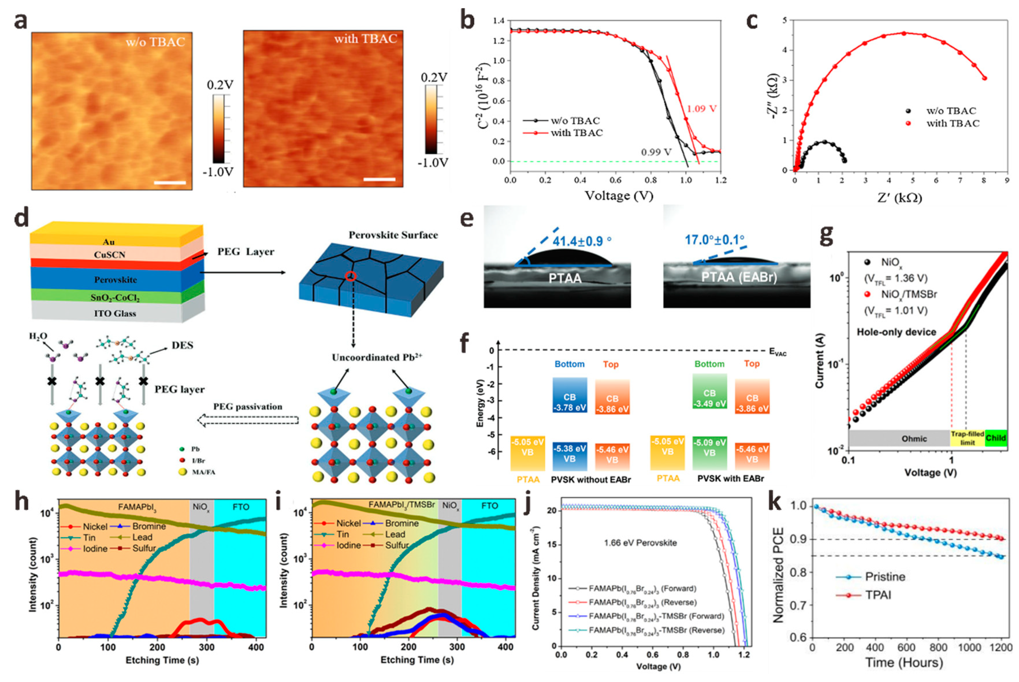
- Shini, F.; Thambidurai, M.; Dewi, H.A.; Jamaludin, N.F.; Bruno, A.; Kanwat, A.; Mathews, N.; Dang, C.; Nguyen, H.D. Interfacial passivation with 4-chlorobenzene sulfonyl chloride for stable and efficient planar perovskite solar cells. J. Mater. Chem. C 2022, 10, 9044–9051. [Google Scholar] [CrossRef]
- Zhong, H.; Jia, Z.; Shen, J.; Yu, Z.; Yin, S.; Liu, X.; Fu, G.; Chen, S.; Yang, S.; Kong, W. Surface treatment of the perovskite via self-assembled dipole layer enabling enhanced efficiency and stability for perovskite solar cells. Appl. Surf. Sci. 2022, 602, 154365. [Google Scholar] [CrossRef]
- Gu, W.-M.; Zhang, Y.; Jiang, K.-J.; Yu, G.; Xu, Y.; Huang, J.-H.; Zhang, Y.; Wang, F.; Li, Y.; Lin, Y.; et al. Surface fluoride management for enhanced stability and efficiency of halide perovskite solar cells via a thermal evaporation method. J. Mater. Chem. A 2022, 10, 12882–12889. [Google Scholar] [CrossRef]
- Xu, S.; Zhang, L.; Liu, B.; Liang, Z.; Xu, H.; Zhang, H.; Ye, J.; Ma, H.; Liu, G.; Pan, X. Constructing of superhydrophobic and intact crystal terminal: Interface sealing strategy for stable perovskite solar cells with efficiency over 23%. Chem. Eng. J. 2023, 453, 139808. [Google Scholar] [CrossRef]
- Wang, X.; Huang, H.; Du, S.; Cui, P.; Lan, Z.; Yang, Y.; Yan, L.; Ji, J.; Liu, B.; Qu, S.; et al. Facile Synthesized Acetamidine Thiocyanate with Synergistic Passivation and Crystallization for Efficient Perovskite Solar Cells. Sol. RRL 2022, 6, 2200717. [Google Scholar] [CrossRef]
- Liu, W.; Dong, H.; Li, X.; Xia, T.; Zheng, G.; Tian, N.; Mo, S.; Peng, Y.; Yang, Y.; Yao, D.; et al. Interfacial Engineering Based on Polyethylene Glycol and Cuprous Thiocyanate Layers for Efficient and Stable Perovskite Solar Cells. Adv. Mater. Interfaces 2022, 9, 2201437. [Google Scholar] [CrossRef]
- Ren, J.; Liu, T.; He, B.; Wu, G.; Gu, H.; Wang, B.; Li, J.; Mao, Y.; Chen, S.; Xing, G. Passivating Defects at the Bottom Interface of Perovskite by Ethylammonium to Improve the Performance of Perovskite Solar Cells. Small 2022, 18, 2203536. [Google Scholar] [CrossRef]
- Wu, T.; Ono, L.K.; Yoshioka, R.; Ding, C.; Zhang, C.; Mariotti, S.; Zhang, J.; Mitrofanov, K.; Liu, X.; Segawa, H.; et al. Elimination of light-induced degradation at the nickel oxide-perovskite heterojunction by aprotic sulfonium layers towards long-term operationally stable inverted perovskite solar cells. Energy Environ. Sci. 2022, 15, 4612–4624. [Google Scholar] [CrossRef]
- Liu, D.; Chen, M.; Wei, Z.; Zou, C.; Liu, X.; Xie, J.; Li, Q.; Yang, S.; Hou, Y.; Yang, H.G. Strain-free hybrid perovskite films based on a molecular buffer interface for efficient solar cells. J. Mater. Chem. A 2022, 10, 10865–10871. [Google Scholar] [CrossRef]
- Chen, J.; Seo, J.Y.; Park, N.G. Simultaneous Improvement of Photovoltaic Performance and Stability by In Situ Formation of 2D Perovskite at (FAPbI3)0.88(CsPbBr3)0.12/CuSCN Interface. Adv. Energy Mater. 2018, 8, 1702714. [Google Scholar] [CrossRef]
- Xu, J.; Dai, J.; Dong, H.; Li, P.; Chen, J.; Zhu, X.; Wang, Z.; Jiao, B.; Hou, X.; Li, J.; et al. Surface-tension release in PTAA-based inverted perovskite solar cells. Org. Electron. 2022, 100, 106378. [Google Scholar] [CrossRef]
- Li, Y.; Wang, B.; Liu, T.; Zeng, Q.; Cao, D.; Pan, H.; Xing, G. Interfacial Engineering of PTAA/Perovskites for Improved Crystallinity and Hole Extraction in Inverted Perovskite Solar Cells. ACS Appl. Mater. Interfaces 2022, 14, 3284–3292. [Google Scholar] [CrossRef]
- Boyd, C.C.; Shallcross, R.C.; Moot, T.; Kerner, R.; Bertoluzzi, L.; Onno, A.; Kavadiya, S.; Chosy, C.; Wolf, E.J.; Werner, J.; et al. Overcoming Redox Reactions at Perovskite-Nickel Oxide Interfaces to Boost Voltages in Perovskite Solar Cells. Joule 2020, 4, 1759–1775. [Google Scholar] [CrossRef]
- Mohd Yusoff, A.R.b.; Vasilopoulou, M.; Georgiadou, D.G.; Palilis, L.C.; Abate, A.; Nazeeruddin, M.K. Passivation and process engineering approaches of halide perovskite films for high efficiency and stability perovskite solar cells. Energy Environ. Sci. 2021, 14, 2906–2953. [Google Scholar] [CrossRef]
- Tang, Y.; Gu, Z.; Fu, C.; Xiao, Q.; Zhang, S.; Zhang, Y.; Song, Y. FAPbI3 Perovskite Solar Cells: From Film Morphology Regulation to Device Optimization. Sol. RRL 2022, 6, 2200120. [Google Scholar] [CrossRef]
- Tong, Y.; Najar, A.; Wang, L.; Liu, L.; Du, M.; Yang, J.; Li, J.; Wang, K.; Liu, S.F. Wide-Bandgap Organic-Inorganic Lead Halide Perovskite Solar Cells. Adv. Sci. 2022, 9, 2105085. [Google Scholar] [CrossRef]
- Huang, K.; Feng, X.; Li, H.; Long, C.; Liu, B.; Shi, J.; Meng, Q.; Weber, K.; Duong, T.; Yang, J. Manipulating the Migration of Iodine Ions via Reverse-Biasing for Boosting Photovoltaic Performance of Perovskite Solar Cells. Adv. Sci. 2022, 9, 2204163. [Google Scholar] [CrossRef] [PubMed]
- Zhao, Y.; Yavuz, I.; Wang, M.; Weber, M.H.; Xu, M.; Lee, J.H.; Tan, S.; Huang, T.; Meng, D.; Wang, R.; et al. Suppressing ion migration in metal halide perovskite via interstitial doping with a trace amount of multivalent cations. Nat. Mater. 2022, 21, 1396–1402. [Google Scholar] [CrossRef] [PubMed]
- Rezaee, E.; Zhang, W.; Silva, S.R.P. Solvent Engineering as a Vehicle for High Quality Thin Films of Perovskites and Their Device Fabrication. Small 2021, 17, 2008145. [Google Scholar] [CrossRef] [PubMed]
- Jung, M.; Ji, S.G.; Kim, G.; Seok, S.I. Perovskite precursor solution chemistry: From fundamentals to photovoltaic applications. Chem. Soc. Rev. 2019, 48, 2011–2038. [Google Scholar] [CrossRef] [PubMed]
- Im, J.H.; Lee, C.R.; Lee, J.W.; Park, S.W.; Park, N.G. 6.5% efficient perovskite quantum-dot-sensitized solar cell. Nanoscale 2011, 3, 4088–4093. [Google Scholar] [CrossRef]
- Lee, M.M.; Teuscher, J.; Miyasaka, T.; Murakami, T.N.; Snaith, H.J. Efficient Hybrid Solar Cells Based on Meso-Superstructured Organometal Halide Perovskites. Science 2012, 338, 643–647. [Google Scholar] [CrossRef]
- Wu, Y.; Islam, A.; Yang, X.; Qin, C.; Liu, J.; Zhang, K.; Peng, W.; Han, L. Retarding the crystallization of PbI2 for highly reproducible planar-structured perovskite solar cells via sequential deposition. Energy Environ. Sci. 2014, 7, 2934–2938. [Google Scholar] [CrossRef]
- Jeon, N.J.; Noh, J.H.; Kim, Y.C.; Yang, W.S.; Ryu, S.; Seok, S.I. Solvent engineering for high-performance inorganic-organic hybrid perovskite solar cells. Nat. Mater. 2014, 13, 897–903. [Google Scholar] [CrossRef]
- Hui, W.; Yang, Y.; Xu, Q.; Gu, H.; Feng, S.; Su, Z.; Zhang, M.; Wang, J.; Li, X.; Fang, J.; et al. Red-Carbon-Quantum-Dot-Doped SnO2 Composite with Enhanced Electron Mobility for Efficient and Stable Perovskite Solar Cells. Adv. Mater. 2020, 32, 1906374. [Google Scholar] [CrossRef]
- Yu, R.; Wu, G.; Shi, R.; Ma, Z.; Dang, Q.; Qing, Y.; Zhang, C.; Xu, K.; Tan, Z.A. Multidentate Coordination Induced Crystal Growth Regulation and Trap Passivation Enables over 24% Efficiency in Perovskite Solar Cells. Adv. Energy Mater. 2023, 13, 2203127. [Google Scholar] [CrossRef]
- Chao, L.; Niu, T.; Gao, W.; Ran, C.; Song, L.; Chen, Y.; Huang, W. Solvent Engineering of the Precursor Solution toward Large-Area Production of Perovskite Solar Cells. Adv. Mater. 2021, 33, 2005410. [Google Scholar] [CrossRef]
- Wu, X.; Zheng, Y.; Liang, J.; Zhang, Z.; Tian, C.; Zhang, Z.; Hu, Y.; Sun, A.; Wang, C.; Wang, J.; et al. Green-solvent-processed formamidinium-based perovskite solar cells with uniform grain growth and strengthened interfacial contact via a nanostructured tin oxide layer. Mater. Horiz. 2023, 10, 122–135. [Google Scholar] [CrossRef] [PubMed]
- Fang, Y.; Jiang, Y.; Yang, Z.; Xu, Z.; Wang, Z.; Lu, X.; Gao, X.; Zhou, G.; Liu, J.M.; Gao, J. A Nontoxic NFM Solvent for High-Efficiency Perovskite Solar Cells with a Widened Processing Window. ACS Appl. Mater. Interfaces 2022, 14, 47758–47764. [Google Scholar] [CrossRef] [PubMed]
- Hui, W.; Chao, L.; Lu, H.; Xia, F.; Wei, Q.; Su, Z.; Niu, T.; Tao, L.; Du, B.; Li, D.; et al. Stabilizing black-phase formamidinium perovskite formation at room temperature and high humidity. Science 2021, 371, 1359–1364. [Google Scholar] [CrossRef] [PubMed]
- Bai, S.; Da, P.; Li, C.; Wang, Z.; Yuan, Z.; Fu, F.; Kawecki, M.; Liu, X.; Sakai, N.; Wang, J.T.; et al. Planar perovskite solar cells with long-term stability using ionic liquid additives. Nature 2019, 571, 245–250. [Google Scholar] [CrossRef] [PubMed]
- Ran, J.; Wang, H.; Deng, W.; Xie, H.; Gao, Y.; Yuan, Y.; Yang, Y.; Ning, Z.; Yang, B. Ionic Liquid-Tuned Crystallization for Stable and Efficient Perovskite Solar Cells. Sol. RRL 2022, 6, 2200176. [Google Scholar] [CrossRef]
- Li, L.; Tu, S.; You, G.; Cao, J.; Wu, D.; Yao, L.; Zhou, Z.; Shi, W.; Wang, W.; Zhen, H.; et al. Enhancing performance and stability of perovskite solar cells through defect passivation with a polyamide derivative obtained from benzoxazine-isocyanide chemistry. Chem. Eng. J. 2022, 431, 133951. [Google Scholar] [CrossRef]
- Hu, L.; Li, S.; Zhang, L.; Liu, Y.; Zhang, C.; Wu, Y.; Sun, Q.; Cui, Y.; Zhu, F.; Hao, Y.; et al. Unravelling the role of C60 derivatives as additives into active layers for achieving high-efficiency planar perovskite solar cells. Carbon 2020, 167, 160–168. [Google Scholar] [CrossRef]
- Kim, K.; Wu, Z.; Han, J.; Ma, Y.; Lee, S.; Jung, S.K.; Lee, J.W.; Woo, H.Y.; Jeon, I. Homogeneously Miscible Fullerene inducing Vertical Gradient in Perovskite Thin-Film toward Highly Efficient Solar Cells. Adv. Energy Mater. 2022, 12, 2200877. [Google Scholar] [CrossRef]
- Ahmed, E.; Breternitz, J.; Groh, M.F.; Ruck, M. Ionic liquids as crystallisation media for inorganic materials. CrystEngComm 2012, 14, 4874. [Google Scholar] [CrossRef]
- Marsh, K.N.; Boxall, J.A.; Lichtenthaler, R. Room temperature ionic liquids and their mixtures—A review. Fluid Phase Equilib. 2004, 219, 93–98. [Google Scholar] [CrossRef]
- Shahiduzzaman, M.; Muslih, E.Y.; Hasan, A.K.M.; Wang, L.; Fukaya, S.; Nakano, M.; Karakawa, M.; Takahashi, K.; Akhtaruzzaman, M.; Nunzi, J.-M.; et al. The benefits of ionic liquids for the fabrication of efficient and stable perovskite photovoltaics. Chem. Eng. J. 2021, 411, 128461. [Google Scholar] [CrossRef]
- Niu, T.; Chao, L.; Gao, W.; Ran, C.; Song, L.; Chen, Y.; Fu, L.; Huang, W. Ionic Liquids-Enabled Efficient and Stable Perovskite Photovoltaics: Progress and Challenges. ACS Energy Lett. 2021, 6, 1453–1479. [Google Scholar] [CrossRef]
- Chao, L.; Niu, T.; Gu, H.; Yang, Y.; Wei, Q.; Xia, Y.; Hui, W.; Zuo, S.; Zhu, Z.; Pei, C.; et al. Origin of High Efficiency and Long-Term Stability in Ionic Liquid Perovskite Photovoltaic. Research 2020, 2020, 2616345. [Google Scholar] [CrossRef] [PubMed]
- He, Z.; Xu, C.; Li, L.; Liu, A.; Ma, T.; Gao, L. Highly efficient and stable perovskite solar cells induced by novel bulk organosulfur ammonium. Mater. Today Energy 2022, 26, 101004. [Google Scholar] [CrossRef]
- Tian, J.; Zhang, K.; Xie, Z.; Peng, Z.; Zhang, J.; Osvet, A.; Lüer, L.; Kirchartz, T.; Rau, U.; Li, N.; et al. Quantifying the Energy Losses in CsPbI2Br Perovskite Solar Cells with an Open-Circuit Voltage of up to 1.45 V. ACS Energy Lett. 2022, 7, 4071–4080. [Google Scholar] [CrossRef]
- Li, D.; Xia, T.; Liu, W.; Zheng, G.; Tian, N.; Yao, D.; Yang, Y.; Wang, H.; Long, F. Methylammonium thiocyanate seeds assisted heterogeneous nucleation for achieving high-performance perovskite solar cells. Appl. Surf. Sci. 2022, 592, 153206. [Google Scholar] [CrossRef]
- Shahiduzzaman, M.; Yamamoto, K.; Furumoto, Y.; Kuwabara, T.; Takahashi, K.; Taima, T. Ionic liquid-assisted growth of methylammonium lead iodide spherical nanoparticles by a simple spin-coating method and photovoltaic properties of perovskite solar cells. RSC Adv. 2015, 5, 77495–77500. [Google Scholar] [CrossRef]
- Wang, D.; Zhang, Z.; Huang, T.; She, B.; Liu, B.; Chen, Y.; Wang, L.; Wu, C.; Xiong, J.; Huang, Y.; et al. Crystallization Kinetics Control Enabled by a Green Ionic Liquid Additive toward Efficient and Stable Carbon-Based Mesoscopic Perovskite Solar Cells. ACS Appl. Mater. Interfaces 2022, 14, 9161–9171. [Google Scholar] [CrossRef]
- Li, T.; Pan, Y.; Wang, Z.; Xia, Y.; Chen, Y.; Huang, W. Additive engineering for highly efficient organic–inorganic halide perovskite solar cells: Recent advances and perspectives. J. Mater. Chem. A 2017, 5, 12602–12652. [Google Scholar] [CrossRef]
- Chang, C.Y.; Chu, C.Y.; Huang, Y.C.; Huang, C.W.; Chang, S.Y.; Chen, C.A.; Chao, C.Y.; Su, W.F. Tuning perovskite morphology by polymer additive for high efficiency solar cell. ACS Appl. Mater. Interfaces 2015, 7, 4955–4961. [Google Scholar] [CrossRef]
- Li, X.; Sheng, W.; Duan, X.; Lin, Z.; Yang, J.; Tan, L.; Chen, Y. Defect Passivation Effect of Chemical Groups on Perovskite Solar Cells. ACS Appl. Mater. Interfaces 2022, 14, 34161–34170. [Google Scholar] [CrossRef] [PubMed]
- Kroto, H.W.; Heath, J.R.; O’Brien, S.C.; Curl, R.F.; Smalley, R.E. C60: Buckminsterfullerene. Nature 1985, 318, 162–163. [Google Scholar] [CrossRef]
- Li, C.-Z.; Chueh, C.-C.; Yip, H.-L.; Zou, J.; Chen, W.-C.; Jen, A.K.Y. Evaluation of structure–property relationships of solution-processible fullerene acceptors and their n-channel field-effect transistor performance. J. Mater. Chem. 2012, 22, 14976. [Google Scholar] [CrossRef]
- Menzel, D.; Al-Ashouri, A.; Tejada, A.; Levine, I.; Guerra, J.A.; Rech, B.; Albrecht, S.; Korte, L. Field Effect Passivation in Perovskite Solar Cells by a LiF Interlayer. Adv. Energy Mater. 2022, 12, 2201109. [Google Scholar] [CrossRef]
- Liu, K.; Chen, S.; Wu, J.; Zhang, H.; Qin, M.; Lu, X.; Tu, Y.; Meng, Q.; Zhan, X. Fullerene derivative anchored SnO2 for high-performance perovskite solar cells. Energy Environ. Sci. 2018, 11, 3463–3471. [Google Scholar] [CrossRef]
- Zhang, F.; Zhu, K. Additive Engineering for Efficient and Stable Perovskite Solar Cells. Adv. Energy Mater. 2019, 10, 1902579. [Google Scholar] [CrossRef]
- Xiao, M.; Huang, F.; Huang, W.; Dkhissi, Y.; Zhu, Y.; Etheridge, J.; Gray-Weale, A.; Bach, U.; Cheng, Y.B.; Spiccia, L. A fast deposition-crystallization procedure for highly efficient lead iodide perovskite thin-film solar cells. Angew. Chem. Int. Ed. 2014, 53, 9898–9903. [Google Scholar] [CrossRef]
- Mei, Y.; Sun, M.; Liu, H.; Li, X.; Wang, S. Polymer additive assisted crystallization of perovskite films for high-performance solar cells. Org. Electron. 2021, 96, 106258. [Google Scholar] [CrossRef]
- Wang, Z.; Chen, S.; Gao, X. PTB7 as additive in Anti-solvent to enhance perovskite film surface crystallinity for solar cells with efficiency over 21%. Appl. Surf. Sci. 2022, 575, 151737. [Google Scholar] [CrossRef]
- Mei, D.; Qiu, L.; Chen, L.; Xie, F.; Song, L.; Wang, J.; Du, P.; Xiong, J. Incorporating polyvinyl pyrrolidone in green anti-solvent isopropanol: A facile approach to obtain high efficient and stable perovskite solar cells. Thin Solid Films 2022, 752, 139196. [Google Scholar] [CrossRef]
- Choi, H.; Liu, X.; Kim, H.I.; Kim, D.; Park, T.; Song, S. A Facile Surface Passivation Enables Thermally Stable and Efficient Planar Perovskite Solar Cells Using a Novel IDTT-Based Small Molecule Additive. Adv. Energy Mater. 2021, 11, 2003829. [Google Scholar] [CrossRef]
- Guo, J.; Sun, J.; Hu, L.; Fang, S.; Ling, X.; Zhang, X.; Wang, Y.; Huang, H.; Han, C.; Cazorla, C.; et al. Indigo: A Natural Molecular Passivator for Efficient Perovskite Solar Cells. Adv. Energy Mater. 2022, 12, 2200537. [Google Scholar] [CrossRef]
- Liu, Z.; Ono, L.K.; Qi, Y. Additives in metal halide perovskite films and their applications in solar cells. J. Energy Chem. 2020, 46, 215–228. [Google Scholar] [CrossRef]
- Zhao, F.; Guo, Y.; Yang, P.; Tao, J.; Jiang, J.; Chu, J. Effect of Li-doped TiO2 layer on the photoelectric performance of carbon-based CsPbIBr2 perovskite solar cell. J. Alloys Compd. 2023, 930, 167377. [Google Scholar] [CrossRef]
- Mo, H.; Wang, D.; Chen, Q.; Guo, W.; Maniyarasu, S.; Thomas, A.G.; Curry, R.J.; Li, L.; Liu, Z. Laser-Assisted Ultrafast Fabrication of Crystalline Ta-Doped TiO2 for High-Humidity-Processed Perovskite Solar Cells. ACS Appl. Mater. Interfaces 2022, 14, 15141–15153. [Google Scholar] [CrossRef] [PubMed]
- Deng, J.; Zhang, H.; Wei, K.; Xiao, Y.; Zhang, C.; Yang, L.; Zhang, X.; Wu, D.; Yang, Y.; Zhang, J. Molecular Bridge Assisted Bifacial Defect Healing Enables Low Energy Loss for Efficient and Stable Perovskite Solar Cells. Adv. Funct. Mater. 2022, 32, 2209516. [Google Scholar] [CrossRef]
- Luo, T.; Ye, G.; Chen, X.; Wu, H.; Zhang, W.; Chang, H. F-doping-Enhanced Carrier Transport in the SnO2/Perovskite Interface for High-Performance Perovskite Solar Cells. ACS Appl. Mater. Interfaces 2022, 14, 42093–42101. [Google Scholar] [CrossRef]
- Ma, H.; Wang, M.; Wang, Y.; Dong, Q.; Liu, J.; Yin, Y.; Zhang, J.; Pei, M.; Zhang, L.; Cai, W.; et al. Asymmetric organic diammonium salt buried in SnO2 layer enables fast carrier transfer and interfacial defects passivation for efficient perovskite solar cells. Chem. Eng. J. 2022, 442, 136291. [Google Scholar] [CrossRef]
- Chen, J.; Dong, H.; Li, J.; Zhu, X.; Xu, J.; Pan, F.; Xu, R.; Xi, J.; Jiao, B.; Hou, X.; et al. Solar Cell Efficiency Exceeding 25% through Rb-Based Perovskitoid Scaffold Stabilizing the Buried Perovskite Surface. ACS Energy Lett. 2022, 7, 3685–3694. [Google Scholar] [CrossRef]
- Venu Rajendran, M.; Ganesan, S.; Sudhakaran Menon, V.; Raman, R.K.; Alagumalai, A.; Ashok Kumar, S.; Krishnamoorthy, A. Manganese Dopant-Induced Isoelectric Point Tuning of ZnO Electron Selective Layer Enable Improved Interface Stability in Cesium–Formamidinium-Based Planar Perovskite Solar Cells. ACS Appl. Energy Mater. 2022, 5, 6671–6686. [Google Scholar] [CrossRef]
- Jiang, Q.; Zhang, L.; Wang, H.; Yang, X.; Meng, J.; Liu, H.; Yin, Z.; Wu, J.; Zhang, X.; You, J. Enhanced electron extraction using SnO2 for high-efficiency planar-structure HC(NH2)2PbI3-based perovskite solar cells. Nat. Energy 2016, 2, 16177. [Google Scholar] [CrossRef]
- Che, Z.; Zhang, L.; Shang, J.; Wang, Q.; Zhou, Y.; Zhou, Y.; Liu, F. Organic ammonium chloride salt incorporated SnO2 electron transport layers for improving the performance of perovskite solar cells. Sustain. Energy Fuels 2022, 6, 3416–3424. [Google Scholar] [CrossRef]
- Arshad, Z.; Wageh, S.; Maiyalagan, T.; Ali, M.; Arshad, U.; Noor-ul, A.; Qadir, M.B.; Mateen, F.; Al-Sehemi, A.G. Enhanced charge transport characteristics in zinc oxide nanofibers via Mg2+ doping for electron transport layer in perovskite solar cells and antibacterial textiles. Ceram. Int. 2022, 48, 24363–24371. [Google Scholar] [CrossRef]
- Adnan, M.; Usman, M.; Ali, S.; Javed, S.; Islam, M.; Akram, M.A. Aluminum Doping Effects on Interface Depletion Width of Low Temperature Processed ZnO Electron Transport Layer-Based Perovskite Solar Cells. Front. Chem. 2021, 9, 795291. [Google Scholar] [CrossRef]
- Yang, W.S.; Park, B.-W.; Jung, E.H.; Jeon, N.J.; Kim, Y.C.; Lee, D.U.; Shin, S.S.; Seo, J.; Kim, E.K.; Noh, J.H.; et al. Iodide management in formamidinium-lead-halide-based perovskite layers for efficient solar cells. Science 2017, 356, 1376–1379. [Google Scholar] [CrossRef] [PubMed]
- Min, H.; Ji, S.-G.; Seok, S.I. Relaxation of externally strained halide perovskite thin layers with neutral ligands. Joule 2022, 6, 2175–2185. [Google Scholar] [CrossRef]
- Chen, Z.; Li, Y.; Liu, Z.; Shi, J.; Yu, B.; Tan, S.; Cui, Y.; Tan, C.; Tian, F.; Wu, H.; et al. Reconfiguration toward Self-Assembled Monolayer Passivation for High-Performance Perovskite Solar Cells. Adv. Energy Mater. 2023, 13, 2202799. [Google Scholar] [CrossRef]
- Jeong, M.J.; Moon, C.S.; Lee, S.; Im, J.M.; Woo, M.Y.; Lee, J.H.; Cho, H.; Jeon, S.W.; Noh, J.H. Boosting radiation of stacked halide layer for perovskite solar cells with efficiency over 25%. Joule 2023, 7, 112–127. [Google Scholar] [CrossRef]
- Rong, Y.; Jin, M.; Du, Q.; Shen, Z.; Feng, Y.; Wang, M.; Li, F.; Liu, R.; Li, H.; Chen, C. Simultaneous ambient long-term conductivity promotion, interfacial modification, ion migration inhibition and anti-deliquescence by MWCNT:NiO in spiro-OMeTAD for perovskite solar cells. J. Mater. Chem. A 2022, 10, 22592–22604. [Google Scholar] [CrossRef]
- Yang, H.; Shen, Y.; Zhang, R.; Wu, Y.; Chen, W.; Yang, F.; Cheng, Q.; Chen, H.; Ou, X.; Yang, H.; et al. Composition-Conditioning Agent for Doped Spiro-OMeTAD to Realize Highly Efficient and Stable Perovskite Solar Cells. Adv. Energy Mater. 2022, 12, 2202207. [Google Scholar] [CrossRef]
- Xu, D.; Gong, Z.; Jiang, Y.; Feng, Y.; Wang, Z.; Gao, X.; Lu, X.; Zhou, G.; Liu, J.M.; Gao, J. Constructing molecular bridge for high-efficiency and stable perovskite solar cells based on P3HT. Nat. Commun. 2022, 13, 7020. [Google Scholar] [CrossRef] [PubMed]
- Sun, J.; Zhang, N.; Wu, J.; Yang, W.; He, H.; Huang, M.; Zeng, Y.; Yang, X.; Ying, Z.; Qin, G.; et al. Additive Engineering of the CuSCN Hole Transport Layer for High-Performance Perovskite Semitransparent Solar Cells. ACS Appl. Mater. Interfaces 2022, 14, 52223–52232. [Google Scholar] [CrossRef]
- Wang, J.; Hu, Q.; Li, M.; Shan, H.; Feng, Y.; Xu, Z.-X. Poly(3-hexylthiophene)/Gold Nanorod Composites as Efficient Hole-Transporting Materials for Perovskite Solar Cells. Sol. RRL 2020, 4, 2000109. [Google Scholar] [CrossRef]
- Park, S.; Kim, D.W.; Park, S.Y. Improved Stability and Efficiency of Inverted Perovskite Solar Cell by Employing Nickel Oxide Hole Transporting Material Containing Ammonium Salt Stabilizer. Adv. Funct. Mater. 2022, 32, 2200437. [Google Scholar] [CrossRef]
- Liang, J.-W.; Firdaus, Y.; Azmi, R.; Faber, H.; Kaltsas, D.; Kang, C.H.; Nugraha, M.I.; Yengel, E.; Ng, T.K.; De Wolf, S.; et al. Cl2-Doped CuSCN Hole Transport Layer for Organic and Perovskite Solar Cells with Improved Stability. ACS Energy Lett. 2022, 7, 3139–3148. [Google Scholar] [CrossRef]
- Yue, X.; Zhao, X.; Fan, B.; Yang, Y.; Yan, L.; Qu, S.; Huang, H.; Zhang, Q.; Yan, H.; Cui, P.; et al. Surface Regulation through Dipolar Molecule Boosting the Efficiency of Mixed 2D/3D Perovskite Solar Cell to 24%. Adv. Funct. Mater. 2023, 33, 2209921. [Google Scholar] [CrossRef]
- Guan, N.; Zhang, Y.; Chen, W.; Jiang, Z.; Gu, L.; Zhu, R.; Yadav, D.; Li, D.; Xu, B.; Cao, L.; et al. Deciphering the Morphology Change and Performance Enhancement for Perovskite Solar Cells Induced by Surface Modification. Adv. Sci. 2023, 10, 2205342. [Google Scholar] [CrossRef]
- Zhang, C.; Shen, X.; Chen, M.; Zhao, Y.; Lin, X.; Qin, Z.; Wang, Y.; Han, L. Constructing a Stable and Efficient Buried Heterojunction via Halogen Bonding for Inverted Perovskite Solar Cells. Adv. Energy Mater. 2023, 13, 2203250. [Google Scholar] [CrossRef]
- Wang, J.; Wang, Z.; Chen, S.; Jiang, N.; Yuan, L.; Zhang, J.; Duan, Y. Reduced Surface Hydroxyl and Released Interfacial Strain by Inserting CsF Anchor Interlayer for High-Performance Perovskite Solar Cells. Sol. RRL 2023, 7, 2200960. [Google Scholar] [CrossRef]
- Zhang, K.; Zhao, G.; Ye, L.; Jia, N.; Liu, C.; Liu, S.; Ye, Q.; Wang, H. Bionic Levodopa-Modified TiO2 for Preparation of Perovskite Solar Cells with Efficiency over 23%. ACS Sustain. Chem. Eng. 2022, 10, 16055–16063. [Google Scholar] [CrossRef]
- Niu, Y.; He, D.; Zhang, X.; Hu, L.; Huang, Y. Enhanced Perovskite Solar Cell Stability and Efficiency via Multi-Functional Quaternary Ammonium Bromide Passivation. Adv. Mater. Interfaces 2023, 10, 2201497. [Google Scholar] [CrossRef]
- Su, R.; Yang, X.; Ji, W.; Zhang, T.; Zhang, L.; Wang, A.; Jiang, Z.; Chen, Q.; Zhou, Y.; Song, B. Additive-associated antisolvent engineering of perovskite films for highly stable and efficient p–i–n perovskite solar cells. J. Mater. Chem. C 2022, 10, 18303–18311. [Google Scholar] [CrossRef]
- Zhang, Y.; Chen, W.; Su, K.; Huang, Y.-Q.; Brooks, K.; Kinge, S.; Zhang, B.; Feng, Y.; Nazeeruddin, M.K. Bifunctional additive 2-amino-3-hydroxypyridine for stable and high-efficiency tin-lead perovskite solar cells. J. Mater. Chem. C 2023, 11, 151–160. [Google Scholar]
- Xu, P.; Xie, L.; Yang, S.; Han, B.; Liu, J.; Chen, J.; Liu, C.; Jia, R.; Yang, M.; Ge, Z. Manipulating Halide Perovskite Passivation by Controlling Amino Acid Derivative Isoelectric Point for Stable and Efficient Inverted Perovskite Solar Cells. Sol. RRL 2023, 7, 2200858. [Google Scholar] [CrossRef]
- Li, Y.; Shi, B.; Gao, F.; Wu, Y.; Lu, C.; Cai, X.; Li, J.; Zhang, C.; Liu, S.F. 2-Fluoro-4-iodoaniline passivates the surface of perovskite films to enhance photovoltaic properties. Appl. Surf. Sci. 2023, 612, 155787. [Google Scholar] [CrossRef]
- Ni, M.; Qi, L. Orotic Acid as a Bifunctional Additive for Regulating Crystallization and Passivating Defects toward High-Performance Formamidinium-Cesium Perovskite Solar Cells. ACS Appl. Mater. Interfaces 2022, 14, 53808–53818. [Google Scholar] [CrossRef]
- Li, Y.; Liu, L.; Zheng, C.; Liu, Z.; Chen, L.; Yuan, N.; Ding, J.; Wang, D.; Liu, S. Plant-Derived l-Theanine for Ultraviolet/Ozone Resistant Perovskite Photovoltaics. Adv. Energy Mater. 2023, 13, 2203190. [Google Scholar] [CrossRef]
- Xu, Y.; Xiong, S.; Jiang, S.; Yang, J.; Li, D.; Wu, H.; You, X.; Zhang, Y.; Ma, Z.; Xu, J.; et al. Synchronous Modulation of Defects and Buried Interfaces for Highly Efficient Inverted Perovskite Solar Cells. Adv. Energy Mater. 2023, 13, 2203505. [Google Scholar] [CrossRef]
- Huang, J.; Wang, H.; Chen, C.; Liu, S. Enhancement of CsPbI3 perovskite solar cells with dual functional passivator 4-Fluoro-3-phenoxybenzaldehyde. Surf. Interfaces 2022, 35, 102477. [Google Scholar] [CrossRef]
- Liu, B.; Wang, Y.; Wu, Y.; Zhang, Y.; Lyu, J.; Liu, Z.; Bian, S.; Bai, X.; Xu, L.; Zhou, D.; et al. Vitamin Natural Molecule Enabled Highly Efficient and Stable Planar n–p Homojunction Perovskite Solar Cells with Efficiency Exceeding 24.2%. Adv. Energy Mater. 2023, 13, 2203352. [Google Scholar] [CrossRef]
- Park, H.; Heo, J.; Jeong, B.H.; Lee, J.; Park, H.J. Interface engineering of organic hole transport layer with facile molecular doping for highly efficient perovskite solar cells. J. Power Sources 2023, 556, 232428. [Google Scholar] [CrossRef]
- Cheng, N.; Cao, Y.; Li, W.; Yu, Z.; Liu, Z.; Lei, B.; Zi, W.; Xiao, Z.; Tu, Y.; Rodríguez-Gallegos, C.D. SnO2 electron transport layer modified with gentian violet for perovskite solar cells with enhanced performance. Org. Electron. 2022, 108, 106600. [Google Scholar] [CrossRef]
- Shang, X.; Ma, X.; Meng, F.; Ma, J.; Yang, L.; Li, M.; Gao, D.; Chen, C. Zwitterionic ionic liquid synergistically induces interfacial dipole formation and traps state passivation for high-performance perovskite solar cells. J. Colloid Interface Sci. 2023, 630, 155–163. [Google Scholar] [CrossRef] [PubMed]
- Zhuang, Q.; Wang, H.; Zhang, C.; Gong, C.; Li, H.; Chen, J.; Zang, Z. Ion diffusion-induced double layer doping toward stable and efficient perovskite solar cells. Nano Res. 2022, 15, 5114–5122. [Google Scholar] [CrossRef]
- Yu, B.; Yu, H.; Sun, Y.; Zhang, J. Dual-layer synergetic optimization of high-efficiency planar perovskite solar cells using nitrogen-rich nitrogen carbide as an additive. J. Mater. Chem. A 2022, 10, 21390–21400. [Google Scholar] [CrossRef]


| Strategy | Passivator | Processing | VOC [V] | JSC [mA cm−2] | FF [%] | PCE [%] | Ntrap [cm−3] | Ref. |
|---|---|---|---|---|---|---|---|---|
| Interface Engineering | TFPhFACl | Control | 1.08 | 25.49 | 79.77 | 21.90 | 3.58 × 10¹⁵ | [127] |
| Passivated | 1.16 | 25.42 | 81.26 | 24.00 | 1.44 × 10¹⁴ | |||
| Interface Engineering | BTACl | Control | 1.08 | 23.78 | 71.74 | 18.43 | 2.74 × 10¹⁶ | [128] |
| Passivated | 1.19 | 23.85 | 76.54 | 21.72 | 1.41 × 10¹⁶ | |||
| Interface Engineering | I-TFBA | Control | 1.13 | 21.80 | 79.20 | 19.50 | 1.43 × 10¹⁶ | [129] |
| Passivated | 1.18 | 22.80 | 82.20 | 22.02 | 1.14 × 10¹⁶ | |||
| Interface Engineering | CsF | Control | 1.15 | 25.28 | 75.32 | 21.93 | 9.67 × 10¹⁵ | [130] |
| Passivated | 1.18 | 25.47 | 77.31 | 23.13 | 4.83 × 10¹⁵ | |||
| Interface Engineering | LDA-Cl | Control | 1.09 | 25.30 | 79.47 | 21.91 | 5.51 × 10¹⁶ | [131] |
| Passivated | 1.13 | 25.46 | 80.69 | 23.28 | 5.09 × 10¹⁶ | |||
| Interface Engineering | BDDAB | Control | 1.06 | 23.96 | 75.95 | 19.39 | 3.41 × 10¹⁵ | [132] |
| Passivated | 1.10 | 24.98 | 80.10 | 22.08 | 1.15 × 10¹⁵ | |||
| Perovskite Surface Treatment | Taurine | Control | 1.07 | 23.94 | 77.00 | 19.73 | 1.13 × 10¹⁵ | [133] |
| Passivated | 1.13 | 24.72 | 80.20 | 22.54 | 4.70 × 10¹⁴ | |||
| Perovskite Surface Treatment | AHPD | Control | 0.69 | 30.68 | 74.18 | 15.72 | 1.40 × 10¹³ | [134] |
| Passivated | 0.81 | 30.03 | 79.10 | 19.18 | 7.80 × 10¹² | |||
| Perovskite Surface Treatment | L-arginine | Control | 1.13 | 22.98 | 78.56 | 20.37 | 9.98 × 10¹³ | [135] |
| Passivated | 1.18 | 23.57 | 82.36 | 22.96 | 3.58 × 10¹⁵ | |||
| Perovskite Surface Treatment | FID | Control | 1.08 | 25.31 | 76.80 | 21.07 | 1.29 × 10¹⁶ | [136] |
| Passivated | 1.14 | 25.42 | 81.00 | 23.44 | 8.85 × 10¹⁵ | |||
| Perovskite Surface Treatment | ORO | Control | 1.05 | 24.55 | 75.36 | 19.47 | 1.90 × 10¹⁶ | [137] |
| Passivated | 1.09 | 24.66 | 76.47 | 20.62 | 1.20 × 10¹⁶ | |||
| Perovskite Surface Treatment | L-Theanine | Control | 1.15 | 25.10 | 76.99 | 22.29 | 1.73 × 10¹⁶ | [138] |
| Passivated | 1.19 | 25.13 | 81.87 | 24.58 | 0.73 × 10¹⁶ | |||
| Perovskite Surface Treatment | DA | Control | 1.07 | 22.33 | 79.59 | 19.04 | 8.50 × 10¹⁵ | [139] |
| Passivated | 1.13 | 23.36 | 83.92 | 22.15 | 3.80 × 10¹⁵ | |||
| Perovskite Surface Treatment | PB | Control | 0.98 | 18.68 | 74.00 | 13.55 | 4.04 × 10¹⁶ | [140] |
| Passivated | 1.09 | 21.02 | 79.00 | 18.01 | 2.04 × 10¹⁶ | |||
| Perovskite Surface Treatment | VC | Control | 1.16 | 24.95 | 78.46 | 22.67 | 3.27 × 10¹⁶ | [141] |
| Passivated | 1.16 | 25.00 | 79.34 | 23.01 | 1.55 × 10¹⁶ | |||
| Dopant Passivation | F4-TCNQ | Control | 1.09 | 22.55 | 73.49 | 18.06 | 3.99 × 10¹⁵ | [142] |
| Passivated | 1.11 | 23.70 | 78.58 | 20.67 | 1.16 × 10¹⁵ | |||
| Dopant Passivation | GV | Control | 1.06 | 22.28 | 68.28 | 16.25 | 9.76 × 10¹⁵ | [143] |
| Passivated | 1.09 | 23.33 | 75.73 | 19.20 | 7.17 × 10¹⁵ | |||
| Dopant Passivation | IMBF4 | Control | 1.09 | 24.66 | 75.07 | 20.18 | 1.96 × 10¹⁵ | [144] |
| Passivated | 1.15 | 24.90 | 80.50 | 23.05 | 1.59 × 10¹⁵ | |||
| Dopant Passivation | LiOH | Control | 1.15 | 22.90 | 73.27 | 19.26 | 3.54 × 10¹⁵ | [145] |
| Passivated | 1.15 | 24.20 | 76.26 | 21.31 | 2.83 × 10¹⁵ | |||
| Dopant Passivation | g-C3N5 | Control | 1.16 | 22.51 | 73.84 | 19.28 | 2.04 × 10¹⁶ | [146] |
| Passivated | 1.18 | 23.97 | 78.98 | 22.34 | 6.82 × 10¹⁵ |
Disclaimer/Publisher’s Note: The statements, opinions and data contained in all publications are solely those of the individual author(s) and contributor(s) and not of MDPI and/or the editor(s). MDPI and/or the editor(s) disclaim responsibility for any injury to people or property resulting from any ideas, methods, instructions or products referred to in the content. |
© 2023 by the authors. Licensee MDPI, Basel, Switzerland. This article is an open access article distributed under the terms and conditions of the Creative Commons Attribution (CC BY) license (https://creativecommons.org/licenses/by/4.0/).
Share and Cite
Du, B.; He, K.; Zhao, X.; Li, B. Defect Passivation Scheme toward High-Performance Halide Perovskite Solar Cells. Polymers 2023, 15, 2010. https://doi.org/10.3390/polym15092010
Du B, He K, Zhao X, Li B. Defect Passivation Scheme toward High-Performance Halide Perovskite Solar Cells. Polymers. 2023; 15(9):2010. https://doi.org/10.3390/polym15092010
Chicago/Turabian StyleDu, Bin, Kun He, Xiaoliang Zhao, and Bixin Li. 2023. "Defect Passivation Scheme toward High-Performance Halide Perovskite Solar Cells" Polymers 15, no. 9: 2010. https://doi.org/10.3390/polym15092010
APA StyleDu, B., He, K., Zhao, X., & Li, B. (2023). Defect Passivation Scheme toward High-Performance Halide Perovskite Solar Cells. Polymers, 15(9), 2010. https://doi.org/10.3390/polym15092010