
Additive Manufacturing of Sensors for Military Monitoring Applications


Abstract
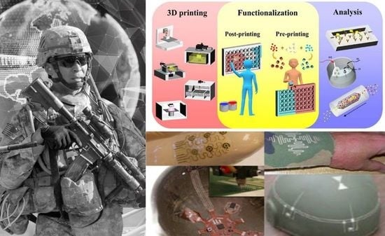
1. Introduction
2. Fabrication of Sensors
2.1. Conventional Manufacturing of Strain Sensors
2.2. 3DP of Biomedical Sensors and Analytical Devices
3. Sensors for Military Applications
3.1. Chemical Sensors
3.2. Biological Sensors
4. 3D Printing Biomedical Devices to Transform Military Medicine
Multimaterial 3DP for Soldiers
5. Conclusions, Challenges and Future Opportunities
Author Contributions
Funding
Institutional Review Board Statement
Informed Consent Statement
Data Availability Statement
Acknowledgments
Conflicts of Interest
References
- Xu, Y.; Wu, X.; Guo, X.; Kong, B.; Zhang, M.; Qian, X.; Mi, S.; Sun, W. The Boom in 3D-Printed Sensor Technology. Sensors 2017, 17, 1166. [Google Scholar] [CrossRef]
- Interview: How the US Army’s Scientists are 3D Printing Cyberpunk-style Biological Sensors. Available online: https://3dprintingindustry.com/news/interview-how-the-us-armys-scientists-are-3d-printing-cyberpunk-style-biological-sensors-178426/ (accessed on 27 November 2020).
- Aerosol Jet Emerging Applications. Available online: https://optomec.com/printed-electronics/aerosol-jet-emerging-applications/military-aerospace/ (accessed on 27 February 2021).
- Han, T.; Kundu, S.; Nag, A.; Xu, Y. 3D Printed Sensors for Biomedical Applications: A Review. Sensors 2019, 19, 1706. [Google Scholar] [CrossRef] [PubMed]
- Afsarimanesh, N.; Nag, A.; Sarkar, S.; Sabet, G.S.; Han, T.; Mukhopadhyay, S.C. A review on fabrication, characterization and implementation of wearable strain sensors. Sens. Actuators A 2020, 315, 112355. [Google Scholar] [CrossRef]
- Nag, A.; Simorangkir, R.B.V.B.; Valentin, E.; Bjorninen, T.; Ukkonen, L.; Hashmi, R.M.; Mukhopadhyay, S.C. A Transparent Strain Sensor Based on PDMS-Embedded Conductive Fabric for Wearable Sensing Applications. IEEE Access 2018, 6, 71020–71027. [Google Scholar] [CrossRef]
- Amjadi, M.; Park, I. Carbon nanotubes-ecoflex nanocomposite for strain sensing with ultra-high stretchability. In Proceedings of the 2015 28th IEEE International Conference on Micro Electro Mechanical Systems (MEMS), Estoril, Portugal, 18–22 January 2015; pp. 744–747. [Google Scholar]
- Ko, W.; Huang, L.; Lin, K. Green technique solvent-free fabrication of silver nanoparti-cle-carbon nanotube flexible films for wearable sensors. Sens. Actuators A 2021, 317, 112437. [Google Scholar] [CrossRef]
- Zhang, X.M.; Yang, X.L.; Wang, K.Y. Conductive graphene/polydimethylsiloxane nano-composites for flexible strain sensors. J. Mater. Sci. 2019, 30, 19319–19324. [Google Scholar]
- Ni, Y.; Ji, R.; Long, K.; Bu, T.; Chen, K.; Zhuang, S. A review of 3D-printed sensors. Appl. Spectrosc. Rev. 2017, 52, 623–652. [Google Scholar] [CrossRef]
- Su, C.-K. Review of 3D-Printed functionalized devices for chemical and biochemical analysis. Anal. Chim. Acta 2021, 1158, 338348. [Google Scholar] [CrossRef]
- Agarwala, S.; Goh, G.L.; Yap, Y.L.; Yu, H.; Yeong, W.Y.; Tran, T. Development of bendable strain sensor with embedded microchannels using 3D printing. Sens. Actuators A Phys. 2017, 263, 593–599. [Google Scholar] [CrossRef]
- Zhang, J.; Chen, L.; Shen, B.; Wang, Y.; Peng, P.; Tang, F.; Feng, J. Highly transparent, self-healing, injectable and self-adhesive chitosan/polyzwitterion-based double network hydrogel for potential 3D printing wearable strain sensor. Mater. Sci. Eng. C 2020, 117, 111298. [Google Scholar] [CrossRef]
- Lee, W.; Kwon, D.; Chung, B.; Jung, G.Y.; Au, A.; Folch, A.; Jeon, S. Ultrarapid Detection of Pathogenic Bacteria Using a 3D Immunomagnetic Flow Assay. Anal. Chem. 2014, 86, 6683–6688. [Google Scholar] [CrossRef]
- Chan, H.N.; Shu, Y.; Xiong, B.; Chen, Y.; Chen, Y.; Tian, Q.; Michael, S.A.; Shen, B.; Wu, H. Simple, Cost-Effective 3D Printed Microfluidic Components for Disposable, Point-of-Care Colorimetric Analysis. ACS Sens. 2015, 1, 227–234. [Google Scholar] [CrossRef]
- Comina, G.; Suska, A.; Filippini, D. Autonomous Chemical Sensing Interface for Universal Cell Phone Readout. Angew. Chem. Int. Ed. 2015, 54, 8708–8712. [Google Scholar] [CrossRef] [PubMed]
- Krejcova, L.; Nejdl, L.; Rodrigo, M.A.M.; Zurek, M.; Matousek, M.; Hynek, D.; Zitka, O.; Kopel, P.; Adam, V.; Kizek, R. 3D printed chip for electrochemical detection of influenza virus labeled with CdS quantum dots. Biosens. Bioelectron. 2014, 54, 421–427. [Google Scholar] [CrossRef]
- Roda, A.; Guardigli, M.; Calabria, D.; Calabretta, M.M.; Cevenini, L.; Michelini, E. A 3D-printed device for a smartphone-based chemiluminescence biosensor for lactate in oral fluid and sweat. Analyst 2014, 139, 6494–6501. [Google Scholar] [CrossRef]
- Forecasting Change in Military Technology, 2020–2040. Available online: https://www.worldpittsburgh.org/wp-content/uploads/2019/01/Forecasting-change-in-military-technology-2020-2040-Brookings-2018.pdf (accessed on 3 January 2021).
- PDID: Pulsed-Discharge Inoization Detector: A New Detector for Medical Diagnosis. Sandia’s Innovation marketplace, A Biannual Update of Available Technologies for Industry, Sandia National Laboratories, March 2019; Volume 5, Issue 1. Available online: https://www.sandia.gov/research/research_foundations/bioscience/_assets/documents/06_Moorman_PDID_MedTech%20Showcase.pdf (accessed on 3 January 2021).
- Technologies to Enable Autonomous Detection for BioWatch. Available online: https://www.nap.edu/read/18495/chapter/3 (accessed on 3 January 2021).
- Kemppinen, O.; Laning, J.C.; Mersmann, R.D.; Videen, G.; Berg, M.J. Imaging atmospheric aerosol particles from a UAV with digital holography. Sci. Rep. 2020, 10, 16085. [Google Scholar] [CrossRef] [PubMed]
- 3D Printed Holography Device Protects Soldiers from Aerosols. Available online: https://3dprinting.com/military/3d-printed-holography-device-protects-soldiers-from-aerosols/ (accessed on 3 January 2021).
- Available online: https://par.nsf.gov/servlets/purl/10113577 (accessed on 3 January 2021).
- Assessment of Wearable Sensor Technologies for Biosurveillance. Available online: http://www.dtic.mil/dtic/tr/fulltext/u2/a611718.pdf (accessed on 3 January 2021).
- Keenan, S.; Riesberg, J. Prolonged Field Care: Beyond the “Golden Hour”. Wildnerness Environ. Med. 2017, 28, S135–S139. [Google Scholar] [CrossRef] [PubMed]
- Farra, R.; Sheppard, N.F.; McCabe, L.; Neer, R.M.; Anderson, J.M.; Santini, J.T.; Cima, M.J.; Langer, R. First-in-Human Testing of a Wirelessly Controlled Drug Delivery Microchip. Sci. Transl. Med. 2012, 4, 122ra21. [Google Scholar] [CrossRef]
- Kong, Y.L.; Gupta, M.K.; Johnson, B.N.; McAlpine, M.C. 3D printed bionic nanodevices. Nano Today 2016, 11, 330–350. [Google Scholar] [CrossRef] [PubMed]
- Awasthi, R.; Kulkarni, G. Decades of research in drug targeting to the upper gastrointestinal tract using gastroretention technologies: Where do we stand? Drug Deliv. 2014, 23, 378–394. [Google Scholar] [CrossRef] [PubMed]
- Kong, Y.L.; Zou, X.; McCandler, C.A.; Kirtane, A.R.; Ning, S.; Zhou, J.; Abid, A.; Jafari, M.; Rogner, J.; Minahan, D.; et al. 3D-Printed Gastric Resident Electronics. Adv. Mater. Technol. 2018, 4, 1800490. [Google Scholar] [CrossRef] [PubMed]
- Ghosh, U.; Ning, S.; Wang, Y.; Kong, Y.L. Addressing Unmet Clinical Needs with 3D Printing Technologies. Adv. Heal. Mater. 2018, 7, e1800417. [Google Scholar] [CrossRef] [PubMed]
- McAlpine, M.C.; Kong, Y.L. 3D Printed Active Electronic Materials and Devices. U.S. Patent 9,887,356, 6 February 2018. [Google Scholar]
- McAlpine, M.C.; Sebastian-Mannoor, M.; Kong, Y.L.; Johnson, B.N. Multi-Functional Hybrid Devices/Structures Using 3D Printing. U.S. Patent 9,517,128, 13 December 2016. [Google Scholar]
- Langer, R.; Traverso, G.; Kong, Y.L. Gastric Resident Electronics. U.S. Patent 16/202,647, 11 July 2019. [Google Scholar]
- Khosravani, M.R.; Reinicke, T. 3D-printed sensors: Current progress and future challenges. Sens. Actuators A Phys. 2020, 305, 111916. [Google Scholar] [CrossRef]
- Palmara, G.; Frascella, F.; Roppolo, I.; Chiappone, A.; Chiadò, A. Functional 3D printing: Approaches and bioapplications. Biosens. Bioelectron. 2021, 175, 112849. [Google Scholar] [CrossRef]
- Miao, S.; Zhu, W.; Castro, N.J.; Nowicki, M.; Zhou, X.; Cui, H.; Fisher, J.P.; Zhang, L.G. 4D printing smart biomedical scaffolds with novel soybean oil epoxidized acrylate. Sci. Rep. 2016, 6, 27226. [Google Scholar] [CrossRef] [PubMed]


| Materials | Type of Sensor | Stretchability (%) |
|---|---|---|
| CNTs-Ecoflex | Resistive | 500 |
| Aligned CNTs-PDMS | Resistive | 280 |
| CNTs-Ecoflex | Capacitive | 150 |
| CNTs-Dragon-skin elastomer | Capacitive | 300 |
| Graphene foam-PDMS | Resistive | 70 |
| CBs-thermoplastic elastomer (TPE) | Resistive | 80 |
| Graphene-rubber | Resistive | 800 |
| AgNWs-PDMS | Resistive | 70 |
| CBs-PDMS | Resistive | 30 |
| Zinc Oxide (ZnO) NWs-PDMS | Resistive | 50 |
| CBs-PDMS | Resistive | 10 |
| CBs-Ecoflex | Resistive | 400 |
| CNTs-silicone elastomer | Capacitive | 100 |
| AgNWs-Ecoflex | Capacitive | 50 |
| Platinum (Pt)-PDMS | Resistive | 2 |
| AuNWs-PANI-rubber | Resistive | 149.6 |
| AgNWs-PEDOT:PSS/PU | Resistive | 100 |
| AuNWs-latex rubber | Resistive | 350 |
| CNTs-PEDOT: PSS/PU | Resistive | 100 |
| 3D Printing Methods | Principle | Materials | Resolution Range (µm) | 3D-Printed Sensor in Biomedical Applications | Advantages | Disadvantages |
|---|---|---|---|---|---|---|
| Fused deposition modelling | Extrusion of constant filament | ABS, PLA, Wax blend, Nylon | x: 100 y: 100 z: 250 | Lactate sensor, cell toxicity sensor, immunosensor, DNA sensor, glucose sensor, bacteria sensor | High speed High quality Used for a wide range of materialDurable over time | Porous structure for the binder Weak mechanical properties Often require support |
| Stereolithography | UV initiated polymerization cross section by cross section | Resin (Acrylate or Epoxy based with proprietary photoinitiator | x: 10 y: 10 z: 15 | DNA imaging sensor, bacteria sensor, cellular sensor | Large parts can be built easily High accuracy and surface finishGood for complex build Simple scalability Uncured material can be reused Improved mechanical properties | Not well-defined mechanical properties due to the usage of photopolymers Slow build process Expensive process Moisture, heat, and chemicals can reduce its durability |
| Polyjet | Deposition of the droplets of the photocurable liquid material and cured | Polymer | x: 30 y: 30 z: 20 | Cell imaging sensor, cell-based sensor (for ATP sensing), physiological sensor, immunosensor | Multiple jetting heads are available to build materials Different levels of flexibility Allows using different colored photopolymers More control over the accuracyHigh accuracy and smooth surface | Vulnerable to heat and humidity Lose strength over time Relatively higher cost compared to others Sharp edges are often slightly rounded |
| Selective laser sintering | Laser-induced sintering of powder particles | Metallic powder, polyamide, PVC | x: 50 y: 50 z: 200 | Cell density sensor | High resolution No support structure is required High strength Less time Complex structures can be easily fabricated | Only metal parts can be printed Finishing or post-processing required due to its grainy roughness Difficulty in the material changeover |
| 3D Inkjet printing | Extrusion of ink and powder liquid binding | Photo-resin or hydrogel | x: 10 y: 10 z: 50 | Bionic ear, multifunctional biomembrane | Very good accuracy Very high surface finishes | Fragile parts Slow build process The grainy or rough appearance Post-processing is required to remove moisture Poor mechanical properties |
| Digital light processing | Photocuring by a digital projector screen to protect layers by squared voxels | Photopolymer and photo-resin | x: 25 y: 25 z: 20 | Piezoelectric acoustic sensor, motion control and soft sensors, glucose sensor | Excellent accuracy of laying High resolution Uncured photopolymer can be reused | Insecurity of the consumable material Difficult to print large structure Boxy surface finish due to its rectangular voxels |
| Technology | Moderate | High | Revolutionary |
|---|---|---|---|
| Sensors | |||
| Chemical sensors | X | ||
| Biological sensors | X | ||
| Optical, infrared, and UV sensors | X | ||
| Radar and radio sensors | X | ||
| Sound, sonar, and motion sensors | X | ||
| Magnetic detection | X | ||
| Particle beams (as sensors) | X | ||
| Computers and communications | |||
| Computer hardware | X | ||
| Computer software | X | ||
| Offensive cyber operations | X | ||
| System of systems/Internet of things | X | ||
| Radio communications | X | ||
| Laser communications | X | ||
| Artificial intelligence/Big data | X | ||
| Quantum computing | X | ||
| Projectiles, propulsion and platforms | |||
| Robotics and autonomous systems | X | ||
| Missiles | X | ||
| Explosives | X | ||
| Fuels | X | ||
| Jet engines | X | ||
| Internal-combustion engines | X | ||
| Battery-powered engines | X | ||
| Rockets | X | ||
| Ships | X | ||
| Armor | X | ||
| Stealth | X | ||
| Satellites | X | ||
| Other weapons and key technologies | |||
| Radio-frequency weapons | X | ||
| Non-lethal weapons | X | ||
| Biological weapons | X | ||
| Chemical weapons | X | ||
| Other weapons of mass destruction | X | ||
| Particle beams (as weapons) | X | ||
| Electric guns, rail guns | X | ||
| Lasers | X | ||
| Nanomaterials | X | ||
| 3D printing (3DP)/Additive manufacturing (AM) | X | ||
| Human enhancement devices and substances | X |
Publisher’s Note: MDPI stays neutral with regard to jurisdictional claims in published maps and institutional affiliations. |
© 2021 by the authors. Licensee MDPI, Basel, Switzerland. This article is an open access article distributed under the terms and conditions of the Creative Commons Attribution (CC BY) license (https://creativecommons.org/licenses/by/4.0/).
Share and Cite
Bird, D.T.; Ravindra, N.M. Additive Manufacturing of Sensors for Military Monitoring Applications. Polymers 2021, 13, 1455. https://doi.org/10.3390/polym13091455
Bird DT, Ravindra NM. Additive Manufacturing of Sensors for Military Monitoring Applications. Polymers. 2021; 13(9):1455. https://doi.org/10.3390/polym13091455
Chicago/Turabian StyleBird, David T., and Nuggehalli M. Ravindra. 2021. "Additive Manufacturing of Sensors for Military Monitoring Applications" Polymers 13, no. 9: 1455. https://doi.org/10.3390/polym13091455
APA StyleBird, D. T., & Ravindra, N. M. (2021). Additive Manufacturing of Sensors for Military Monitoring Applications. Polymers, 13(9), 1455. https://doi.org/10.3390/polym13091455