Electromagnetic Wave Absorption Properties of Structural Conductive ABS Fabricated by Fused Deposition Modeling


Abstract

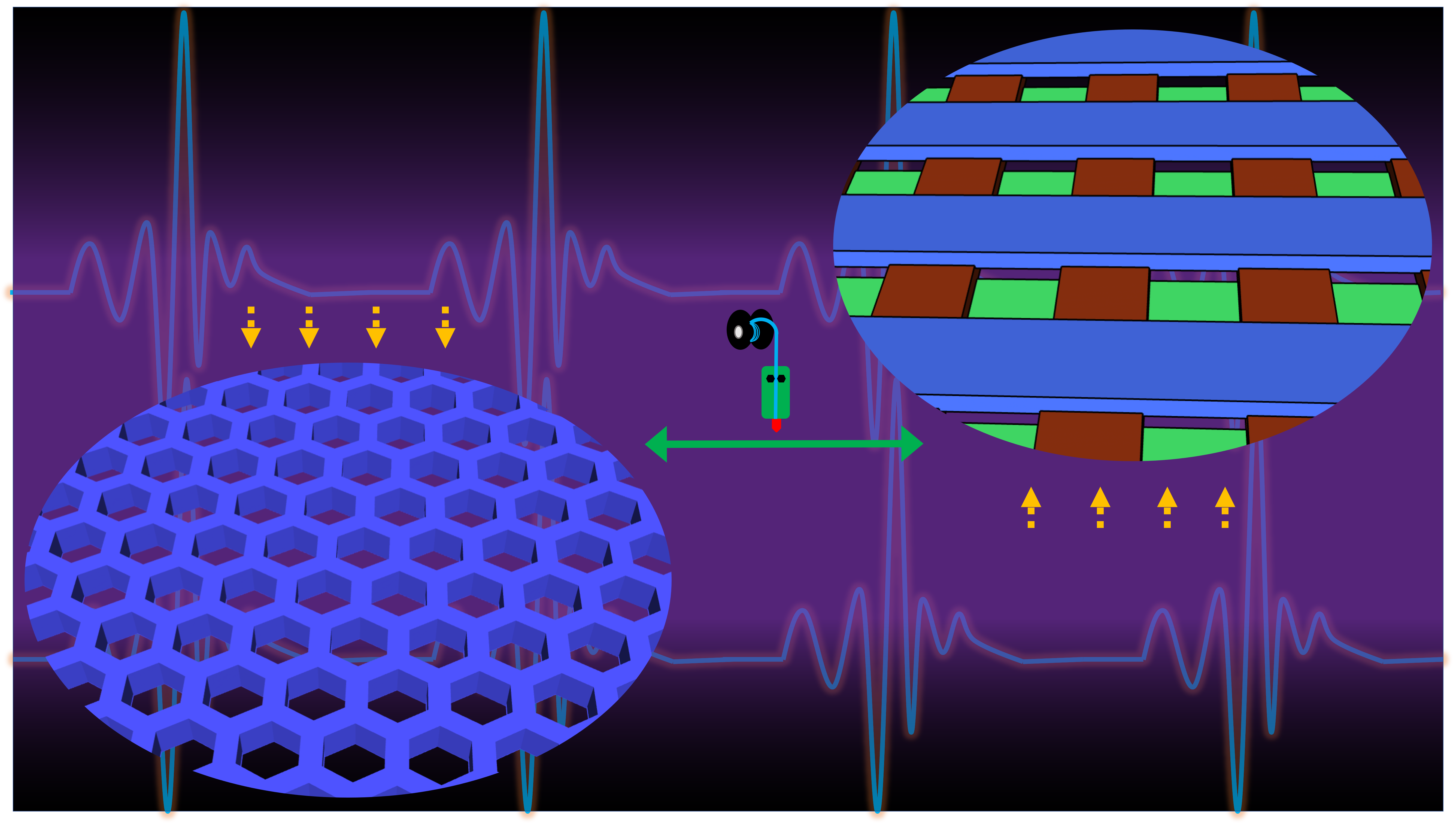
1. Introduction
2. Experimental Setup
2.1. Materials
2.2. Preparation of the Conductive ABS Filaments
2.3. The 3D Printing Process
2.4. Characterization and Testing
2.4.1. Electrical Conductivity Testing
2.4.2. Electromagnetic Parameters Testing
2.4.3. EMW Absorbing Performance Testing
3. Results and Discussions
3.1. Theory of EMW Absorption
3.2. Electromagnetic Property Analyses
3.3. EMW Absorbing Performance Analyses
4. Conclusions
Author Contributions
Funding
Acknowledgments
Conflicts of Interest
References
- Yin, X.; Kong, L.; Zhang, L.; Cheng, L.; Travitzky, N.; Greil, P. Electromagnetic properties of Si–C–N based ceramics and composites. Int. Mater. Rev. 2014, 59, 326–355. [Google Scholar] [CrossRef]
- Chen, Y.; Zhang, H.-B.; Yang, Y.; Wang, M.; Cao, A.; Yu, Z.-Z. High-Performance Epoxy Nanocomposites Reinforced with Three-Dimensional Carbon Nanotube Sponge for Electromagnetic Interference Shielding. Adv. Funct. Mater. 2015, 26, 447–455. [Google Scholar] [CrossRef]
- Cheng, Y.; Tan, M.; Hu, P.; Zhang, X.; Sun, B.; Yan, L.; Zhou, S.; Han, W. Strong and thermostable SiC nanowires/graphene aerogel with enhanced hydrophobicity and electromagnetic wave absorption property. Appl. Surf. Sci. 2018, 448, 138–144. [Google Scholar] [CrossRef]
- Wang, L.; Jia, X.; Li, Y.; Yang, F.; Zhang, L.; Liu, L.; Ren, X.; Yang, H. Synthesis and microwave absorption property of flexible magnetic film based on graphene oxide/carbon nanotubes and Fe3O4 nanoparticles. J. Mater. Chem. A 2014, 2, 14940. [Google Scholar] [CrossRef]
- Zhang, Y.; Li, H.; Yang, X.; Zhang, T.; Zhu, K.; Si, W.; Liu, Z.; Sun, H. Additive manufacturing of carbon nanotube-photopolymer composite radar absorbing materials. Polym. Compos. 2016. [Google Scholar] [CrossRef]
- Kong, L.; Li, Z.W.; Liu, L.; Huang, R.; Abshinova, M.; Yang, Z.; Tang, C.B.; Tan, P.K.; Deng, C.R.; Matitsine, S. Recent progress in some composite materials and structures for specific electromagnetic applications. Int. Mater. Rev. 2013, 58, 203–259. [Google Scholar] [CrossRef]
- Li, R.; He, S.; Chu, W. Research progress in electromagnetic wave absorbing coating materials. Ordn. Mater. Sci. Eng. 2006, 29, 76–80. [Google Scholar]
- Liu, Q.; Cao, Q.; Bi, H.; Liang, C.; Yuan, K.; She, W.; Yang, Y.; Che, R. CoNi@SiO2@TiO2 and CoNi@Air@TiO2 Microspheres with Strong Wideband Microwave Absorption. Adv. Mater. 2015, 28, 486–490. [Google Scholar] [CrossRef]
- He, S.; Wang, G.; Lu, C.; Liu, J.; Wen, B.; Liu, H.; Guo, L.; Cao, M.-S. Enhanced wave absorption of nanocomposites based on the synthesized complex symmetrical CuS nanostructure and poly(vinylidene fluoride). J. Mater. Chem. A 2013, 1, 4685–4692. [Google Scholar] [CrossRef]
- Yang, L.; Cai, H.; Zhang, B.; Huo, S.; Chen, X. Enhanced microwave absorption property of epoxy nanocomposites based on PANI@Fe3O4@CNFs nanoparticles with three-phase heterostructure. Mater. Res. Express 2018, 5, 025304. [Google Scholar] [CrossRef]
- Mohammadkhani, F.; Montazer, M.; Latifi, M. Microwave absorption and photocatalytic properties of magnetic nickel nanoparticles/recycled PET nanofibers web. J. Text. Inst. 2019, 110, 1606–1614. [Google Scholar] [CrossRef]
- Yu, J.; Yu, J.; Ying, T.; Cui, C.; Sun, Y.; Liu, X. The design and the preparation of mesoporous Ag3PO4 nanorod/SrFe12O19 hexagonal nanoflake heterostructure for excellent microwave absorption. J. Alloys Compd. 2019, 775, 225–232. [Google Scholar] [CrossRef]
- Liang, C.; Liu, C.; Wang, H.; Wu, L.; Jiang, Z.; Xu, Y.; Shen, B.; Wang, Z. SiC–Fe3O4 dielectric–magnetic hybrid nanowires: Controllable fabrication, characterization and electromagnetic wave absorption. J. Mater. Chem. A 2014, 2, 16397–16402. [Google Scholar] [CrossRef]
- Liu, X.; Ran, S.; Yu, J.; Sun, Y. Multiscale assembly of Fe2B porous microspheres for large magnetic losses in the gigahertz range. J. Alloys Compd. 2018, 765, 943–950. [Google Scholar] [CrossRef]
- Xu, S.; Sun, Q. Study on absorbing properties of electromagnetic wave oblique incidence on honeycomb-structured absorbing materials. Adv. Aeron. Sci. Eng. 2013, 2, e18. [Google Scholar]
- Park, K.-Y.; Lee, S.-E.; Kim, C.-G.; Han, J.-H. Fabrication and electromagnetic characteristics of electromagnetic wave absorbing sandwich structures. Compos. Sci. Technol. 2006, 66, 576–584. [Google Scholar] [CrossRef]
- Choi, W.-H.; Kim, C.-G. Broadband microwave-absorbing honeycomb structure with novel design concept. Compos. Part B Eng. 2015, 83, 14–20. [Google Scholar] [CrossRef]
- Wu, Y.; Liu, Q.; Fu, J.; Li, Q.; Hui, D. Dynamic crash responses of bio-inspired aluminum honeycomb sandwich structures with CFRP panels. Compos. Part B Eng. 2017, 121, 122–133. [Google Scholar] [CrossRef]
- Nia, A.A.; Sadeghi, M.Z. Te effects of foam filling on compressive response of hexagonal cell aluminum honeycombs under axial loading-experimental study. Mater. Des. 2010, 31, 1216–1230. [Google Scholar]
- Bollen, P.; Quievy, N.; Detrembleur, C.; Thomassin, J.; Monnereau, L.; Bailly, C.; Huynen, I.; Pardoen, T. Processing of a new class of multifunctional hybrid for electromagnetic absorption based on a foam filled honeycomb. Mater. Des. 2016, 89, 323–334. [Google Scholar] [CrossRef]
- Jiang, W.; Yan, L.; Ma, H.; Fan, Y.; Wang, J.; Feng, M.; Qu, S. Electromagnetic wave absorption and compressive behavior of a three-dimensional metamaterial absorber based on 3D printed honeycomb. Sci. Rep. 2018, 8, 4817. [Google Scholar] [CrossRef] [PubMed]
- Zhang, Q.; Yang, X.; Li, P.; Huangab, G.; Feng, S.; Shen, C.; Han, B.; Zhang, X.; Jin, F.; Xu, F.; et al. Bioinspired engineering of honeycomb structure—Using nature to inspire human innovation. Prog. Mater. Sci. 2015, 74, 332–400. [Google Scholar] [CrossRef]
- Han, B.; Qin, K.; Yu, B.; Wang, B.; Zhang, Q.; Lu, T.J. Honeycomb–corrugation hybrid as a novel sandwich core for significantly enhanced compressive performance. Mater. Des. 2016, 93, 271–282. [Google Scholar] [CrossRef]
- Huynen, I.; Bednarz, L.; Thomassin, J.-M.; Pagnoulle, C.; Jérôme, C.; Detrembleur, C. Microwave absorbers based on foamed nanocomposites with graded concentration of carbon nanotubes. In Proceedings of the 2008 38th European Microwave Conference, Amsterdam, The Netherlands, 27–31 October 2008; pp. 5–8. [Google Scholar]
- Gao, Y.; Gao, X.; Li, J.; Guo, S. Microwave absorbing and mechanical properties of alternating multilayer carbonyl iron powder-poly(vinyl chloride) composites. J. Appl. Polym. Sci. 2017, 135, 45846. [Google Scholar] [CrossRef]
- Yin, M.; Tian, X.Y.; Wu, L.L.; Li, D.C. A Broadband and omnidirectional electromagnetic wave concentrator with gradient woodpile structure. Opt. Express 2013, 21, 19082. [Google Scholar] [CrossRef]
- Chen, M.; Zhu, Y.; Pan, Y.; Kou, H.; Xu, H.; Guo, J. Gradient multilayer structural design of CNTs/SiO2 composites for improving microwave absorbing properties. Mater. Des. 2011, 32, 3013–3016. [Google Scholar] [CrossRef]
- Stansbury, J.W.; Idacavage, M.J.; Information, P.E.K.F.C. 3D printing with polymers: Challenges among expanding options and opportunities. Dent. Mater. 2016, 32, 54–64. [Google Scholar] [CrossRef]
- Wang, X.; Jiang, M.; Zhou, Z.; Gou, J.; Hui, D. 3D printing of polymer matrix composites: A review and prospective. Compos. Part B Eng. 2017, 110, 442–458. [Google Scholar] [CrossRef]
- Hart, L.R.; Li, S.; Sturgess, C.; Wildman, R.D.; Jones, J.; Hayes, W. 3D Printing of Biocompatible Supramolecular Polymers and their Composites. ACS Appl. Mater. Interfaces 2016, 8, 3115–3122. [Google Scholar] [CrossRef]
- Muth, J.T.; Vogt, D.M.; Truby, R.L.; Mengüç, Y.; Kolesky, D.B.; Wood, R.J.; Lewis, J.A. Embedded 3D Printing of Strain Sensors within Highly Stretchable Elastomers. Adv. Mater. 2014, 26, 6307–6312. [Google Scholar] [CrossRef]
- Dizon, J.R.C.; Espera, A.H.; Chen, Q.; Advincula, R.C. Mechanical characterization of 3D-printed polymers. Addit. Manuf. 2018, 20, 44–67. [Google Scholar] [CrossRef]
- Caminero, M.Á.; Chacón, J.; García-Plaza, E.; Núñez, P.; Reverte, J.; Becar, J. Additive Manufacturing of PLA-Based Composites Using Fused Filament Fabrication: Effect of Graphene Nanoplatelet Reinforcement on Mechanical Properties, Dimensional Accuracy and Texture. Polymers 2019, 11, 799. [Google Scholar] [CrossRef] [PubMed]
- Ryder, M.A.; Lados, D.A.; Iannacchione, G.S.; Peterson, A.M. Fabrication and properties of novel polymer-metal composites using fused deposition modeling. Compos. Sci. Technol. 2018, 158, 43–50. [Google Scholar] [CrossRef]
- Khatri, B.; Lappe, K.; Habedank, M.; Mueller, T.; Megnin, C.; Hanemann, T. Fused Deposition Modeling of ABS-Barium Titanate Composites: A Simple Route towards Tailored Dielectric Devices. Polymers 2018, 10, 666. [Google Scholar] [CrossRef] [PubMed]
- Kraus, J.D. Helical beam antennas for wide-band applications. Proc. IRE 1948, 36, 1236–1242. [Google Scholar] [CrossRef]
- Tong, G.; Wu, W.; Hua, Q.; Miao, Y.; Guan, J.; Qian, H. Enhanced electromagnetic characteristics of carbon nanotubes/carbonyl iron powders complex absorbers in 2–18 GHz ranges. J. Alloys Compd. 2011, 509, 451–456. [Google Scholar] [CrossRef]
- Guan, P.F.; Zhang, X.F.; Guo, J.J. Assembled Fe3O4 nanoparticles on graphene for enhanced electromagnetic wave losses. Appl. Phys. Lett. 2012, 101, 153108. [Google Scholar] [CrossRef]
- Tong, G.X.; Guan, J.G.; Fan, X.A.; Wang, W.; Li, W. Influences of pyrolysis temperature on static magnetic and microwave electromagnetic properties of polycrystalline iron fibers. Acta Metall. Sin. Chin. Ed. 2008, 44, 867–870. [Google Scholar]
- Mei, H.; Zhao, X.; Zhou, S.; Han, D.; Xiao, S.; Cheng, L. 3D-printed oblique honeycomb Al2O3/SiCw structure for electromagnetic wave absorption. Chem. Eng. J. 2019, 372, 940–945. [Google Scholar] [CrossRef]
- Li, W.; Wu, T.; Wang, W.; Zhai, P. Broadband patterned magnetic microwave absorber. J. Appl. Phys. 2014, 116, 044110. [Google Scholar] [CrossRef]
- Wang, C.J.; Li, J.; Guo, S.Y. High-performance electromagnetic wave absorption by designing the multilayer graphene/thermoplastic polyurethane porous composites with gradient foam ratio structure. Compos. Part A 2019, 125, 105522. [Google Scholar] [CrossRef]


| Properties | Test Methods | Unit | Values |
|---|---|---|---|
| Melt index | ASTM D1238 (200 °C, 5 KG) | g/10 min | |
| Heat deflection temperature | ASTM D648 | °C | |
| Tensile strength | ASTM D638 | kg/cm2 | |
| Impact strength | ASTM D256 | J/m | |
| Conductivity | Shown in 2.4.1 | S/cm |
| Main Printing Parameters | Values |
|---|---|
| Layer height (mm) | 0.1 |
| Infill density (%) | 100 |
| Print speed (mm/s) | 30 |
| Nozzle temperature (°C) | 260 |
| Nozzle diameter (mm) | 0.4 |
| Build platform temperature (°C) | 100 |
| Samples | #1 | #2 | #3 | #4 | #5 |
|---|---|---|---|---|---|
| Apparent density (g/cm3) | 0.49 | 0.53 | 0.51 | 0.56 | 0.57 |
| EAB (RL < −10 dB) (GHz) | 4.97 | 3.86 | 2.13 | 4.52 | 5.43 |
| RL-min (dB) | −18.46 | −23.37 | −16.94 | −28.13 | −22.15 |
© 2020 by the authors. Licensee MDPI, Basel, Switzerland. This article is an open access article distributed under the terms and conditions of the Creative Commons Attribution (CC BY) license (http://creativecommons.org/licenses/by/4.0/).
Share and Cite
Lai, W.; Wang, Y.; He, J. Electromagnetic Wave Absorption Properties of Structural Conductive ABS Fabricated by Fused Deposition Modeling. Polymers 2020, 12, 1217. https://doi.org/10.3390/polym12061217
Lai W, Wang Y, He J. Electromagnetic Wave Absorption Properties of Structural Conductive ABS Fabricated by Fused Deposition Modeling. Polymers. 2020; 12(6):1217. https://doi.org/10.3390/polym12061217
Chicago/Turabian StyleLai, Wenwen, Yan Wang, and Junkun He. 2020. "Electromagnetic Wave Absorption Properties of Structural Conductive ABS Fabricated by Fused Deposition Modeling" Polymers 12, no. 6: 1217. https://doi.org/10.3390/polym12061217
APA StyleLai, W., Wang, Y., & He, J. (2020). Electromagnetic Wave Absorption Properties of Structural Conductive ABS Fabricated by Fused Deposition Modeling. Polymers, 12(6), 1217. https://doi.org/10.3390/polym12061217