1. Introduction
Silicon quantum dots (Si QDs), promising for applications in fluorescence biomarkers because of their low cytotoxicity [
1,
2,
3], have recently shown improved device performance for prototype light emitting diodes (QLEDs) [
4,
5,
6,
7,
8]. Being an indirect band gap semiconductor, silicon has poor optical properties (absorbance and emission), so an optically-excited type of LED is not a good option for use. However, we expect a dramatically improved device performance for a current-driven LED with Si QDs because external quantum efficiency (EQE) should be dominated by recombination rate between electrons and holes injected from electrodes. In fact, the best value of EQE for Si-QLEDs is as high as 8.6%, which is still a record value in cadmium-free QLEDs [
4,
9,
10]. The next important step is the development of an advanced Si-QLED, in addition to achieving an optimized optical performance in terms of low turn-on voltage, high EQE, strong brightness, Gaussian-shaped electroluminescence (EL) spectra, narrow emission band tunable over a wide range from visible to near-infrared (NIR) wavelengths, a long device lifetime, resistance characteristics against humidity and oxidation, no parasitic emission, and spectral stability over a broad range of operation voltages.
In typical QLEDs, a conventional device architecture is used. Indium tin oxide (ITO) is adopted for the anode, while aluminum (Al) is used for the cathode [
11]. QLEDs have a multilayer structure that consists of an electron injection layer (EIL), an electron transportation layer (ETL), an active layer, a hole transportation layer (HTL), and a hole injection layer (HIL). For Si-QLEDs, polyethylene dioxythiophene:polystyrene sulfonate (PEDOT:PSS) and poly TPD serve as the HTL/HIL, while 1,3,5-tris(N-phenylbenzimidazol-2-yl)benzene (TPBi) is usually used as the EIL/ETL. However, there are papers reporting that an organic/inorganic hybrid multilayered structure might exhibit a poor stability against oxygen and moisture in ambient air [
12]. It is also reported that the performance of the hybrid devices degrades over time. The degradation is induced by PEDOT:PSS, leading to the acid corrosion of ITO [
13,
14]. Maier-Flaig et al. studied morphological and compositional changes of Si-QLEDs during device operation [
15]. For this purpose, they employed a combined analysis of cross-sectional transmission electron microscopy (TEM), energy filtered TEM, and energy dispersive X-ray spectroscopic mapping. Their TEM observation revealed that operation of a QLED with a conventional device structure at high applied voltage accelerated the significant morphological changes. Specifically, a strong electro-migration of QDs into the neighboring compositional organic EIL/ETL caused the formation of a large amount of macroscopic defects, leading to the collapse of multilayered structure. As predicted, such an intermixing effect spoiled the hole-blocking performance of the EIL/ETL, leading to the degradation of optical performance. To overcome these shortcomings, scientists have tried replacing the organic layers with inorganic layers to develop QLEDs that work even in a high operation voltage range [
16,
17,
18]. A variety of metal oxides including zinc oxide (ZnO), nickel oxide (NiO), tungsten oxide (WO
3), and molybdenum oxide (MoO
3) have been used till now for carrier injection and transportation layers, resulting in the fabrication of a device that survives for a long operation time even in harsh environments [
19]. More recently, we reported that inverted device structure allows the Si-QLED to demonstrate a stable optical performance even in high electronic fields, in addition to the long-life device stability [
20]. We concluded that the device degradation originating from the intermixing effect could be evitable when the inverted structure is adopted, although the multilayer still contains organic HTL/HIL of 4,4′-bis(carbazole-9-yl)biphenyl (CBP) molecules.
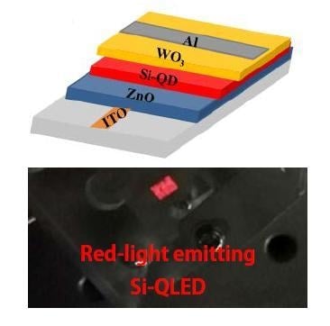
In this study, we report an all-inorganic Si-QLED for the first time. Except for the electrode, the multilayer demonstrated here was fabricated by spin-coating of colloidal inks of nanocrystals including Si QDs.
2. Materials and Methods
2.1. Materials
Triethoxysilane (TES) was purchased from TCI Chemicals (Tokyo, Japan). Electronic grade hydrofluoric acid (49% aqueous solution) was purchased from Kanto Chemical (Tokyo, Japan). HPLC-grade toluene, isopropanol (IPA), ethanol, methanol acetone, ammonia solution (NH4OH, 28-30%), and hydrogen peroxide (H2O2), were purchased from Wako Chemicals (Tokyo, Japan). 1-decene, zinc acetate dehydrate, and WO3 nanoparticle ink (2.5 wt. % in IPA) were purchased from Sigma-Aldrich (St. Louis, MI, USA), and used as received.
2.2. Preparation of Decane-terminated Si QDs
In accordance with our previous protocol [
21], hydrogen-terminated Si QDs were prepared by thermal disproportionation of hydrogen silsesquioxane derived from triethoxysilane, followed by hydrofluoric etching. The hydrogen–silicon surface bonds were replaced by carbon–silicon bonds through thermal hydrosilylation of 1-decene. We observed the enhanced photoluminescence quantum yields (PL QYs) from 0.2% (for hydrogen-termination) to 18% (for decane-termination) as a result of preventing the formation of nonradiative recombination channels in the surface of the QDs [
22]. We call this role of the alkyl monolayer on enhanced PL QY the “anchor effect” [
23]. XRD spectra of the as-prepared Si QDs are shown in
Figure 1a. The peaks at 28°, 47°, and 56° were assigned as the (111), (220), and (311) planes of diamond cubic silicon.
2.3. Fabrication of the Si-QLED
The Si-QLED was prepared on an ITO-coated glass substrate (sheet resistivity ~15 Ω/sq). The substrate was etched in a thin strip and then cleaned by the standard RCA cleaning method which is widely used in the semiconductor industry. Then, 5 parts of Milli-Q water (18.2 MΩ·cm, 50 mL) were mixed with 1 part of NH
4OH (28%, 10 mL) and 1 part of H
2O
2 (30%, 10 mL) and then heated to 70 °C. During heating at a constant temp of 70 °C, the ITO substrate was dipped for 15 min and then rinsed twice in the water. Lastly, to remove the water, the substrate was rinsed with IPA and dried in a heating chamber. After the ozone-cleaning with a deep-UV light, the substrate was transferred to the spin-cast chamber for spin-coating. Colloidal inks of ZnO (20 mg/mL), Si QDs (10 mg/mL), and WO
3 (5 mg/mL) nanocrystals were spin-casted sequentially with rotation speeds of 2000, 1000, and 1000 rpm, respectively. The colloidal ink of ZnO nanocrystals was prepared by following the procedure reported previously [
24]. We used ethanol, toluene, and IPA to prepare colloidal inks of ZnO, Si QD, and WO
3, respectively. The use of the orthogonal solvents enabled the underlying layer to avoid any damage caused by spin-coating over layers. In each step of coating, the films were dried for 1 h at 120 °C in a vacuum chamber. The film thicknesses of ZnO and WO
3 were approximately 22 and 13 nm respectively. The top electrode Al of 150 nm was deposited using a mask by the thermal evaporation technique.
2.4. Characterization
To avoid the solvent effect on PL QYs, optical properties were measured using the QD films deposited onto quartz glass substrates. The PL spectrum was measured by a modular double grating Czerny–Turner monochromator and iHR 320 monochromator (1200 lines/mm of gratings) coupled with a photomultiplier tube (PMT-955) mounted on fluorescence spectrometer (NanoLog Horiba JovinYvon, Kyoto, Japan). A 450 W xenon lamp was used for photoexcitation. The spectral resolution of the spectrofluorometer was ~0.3 nm. The absolute PL QYs were measured at room temperature using the QY measurement system (C11347-11, Hamamatsu Photonics Co. Ltd., Shizuoka, Japan). A 150 W xenon lamp for excitation was mounted on the system. A monochromator for wavelength discrimination, an integrating sphere for a sample chamber, and a multichannel analyzer for signal detection were coupled to the system.
I–V characterization of the device was investigated by a computer programmable Keithley 2400 and 2425. To measure the Si-QLED characteristics, the prototype QLED was kept just above a silicon photodiode to sense the emitted light from the QLED. Photodiode current was measured by the Keithley 2425. EL spectra were measured by collecting the light by an objective lens equipped with a SMA905 connector and sent by optical fiber (ϕ = 1000 μm) to a Si CCD array multichannel monochromator with 2048 pixels (OP-FLAME-S-OW, Ocean Photonic, Ltd., Tokyo, Japan). EQE was calculated as a ratio of the number of forward-emitted photons to the number of injected electrons, expressed as:
where
Nphot is the number of forward-emitted photons which is counted by the photodiode,
Id is the current passing through the device under operation voltage, and |
e| is the magnitude of charge of an electron.
The geometric factor,
g, is expressed as:
where
a is the length and breadth of a square photodiode and
L is the distance between the emitting QLED pixel and the photodiode.
The photodiode current, divided by the responsivity value of the photodiode at the peak energy of the EL spectrum, gives the output photon for light from the device. The number of the photon is calculated by simply dividing with hc/λ. The formula for the EQE calculation is simplified as expressed:
where
I (
photodiode) is the photo current, in which dark current is subtracted, detected by a photodiode (Hamamatsu S1336-8BQ, Shizuoka, Japan) placed just below the EL device.
I (
device) is the device current, when the device is not operative. R is the responsivity of the photodiode and g is the configuration factor of our measurement set-up, which we estimated was 4.
Luminance (Cd/m
2) was estimated using the value of EQE and the area of the EL spectrum, as expressed:
3. Results and Discussion
Figure 1b,c schematically illustrate the inverted QLED (i.e., ITO/ZnO/Si/WO
3/Al) as well as its flat energy band diagram. In contrast to a conventional structure, the electrons were injected from the ITO electrode while the holes were injected from the Al electrode in the inverted device structure, as indicated by arrows in
Figure 1b. With an electron affinity of 4.3 eV and an ionization potential of 7.6 eV [
25], the ZnO EIL/ETL worked for efficient electron injection from the ITO electrode into an active layer of Si QDs. The layer of ZnO also worked for confinement of holes within the active layer because of the valence band offset at the ZnO/QD interface. Both effects strengthened the carrier recombination efficiency. On the other hand, the WO
3 HIL/HTL provided a deep level of the highest occupied molecular orbital (HOMO) (7 eV) which was helpful for hole injection in the HOMO level of the Si QD (5.5 eV) [
26].
Electrical characterization of the QLED is provided in
Figure 2. I–V characteristics of the device and photodiode have been plotted in
Figure 2a. The QLED showed good rectification behavior. Current density–voltage (J–V) characteristics were replotted in a log–log scale in
Figure 2b. The experimental data was linearly fitted to reveal the power law relation J∝V
n where the value of n was a signature of the conduction mechanism. In
Figure 2b, J–V characteristics were fitted with two linear functions. The first one was seen in a low voltage region (0–0.5 V), while another one was seen in a high voltage region (0.5–3 V). In the low voltage region, the relation was J∝V
1.9, indicative of trap free space-charge-limited conduction (SCL). The SCL current appeared at the same time as the injected carrier density exceeded the density of carriers produced by thermal excitation. In the absence of any traps for carriers, the ideal SCL current density is given by the Mott–Gurney Law, J∝V
2 [
6]. While in the high voltage range, the value of exponent (at high current) increased and the relation became J∝V
5.2 which indicated the appearance of the SCLC mechanism with exponential distribution of traps [
16,
27]. The increase in the J–V slope at ~3 V coincided with the photodiode attached just below the active device giving the response when the Si-QLED started emitting light. So, the estimated value of turn-on voltage was as low as 3 V.
The values of EQE for our Si-QLEDs are plotted in
Figure 3a as a function of the injected current density. EQE reached a maximum value of 0.25 % at a current density 0.00125 A/cm
2. With increasing the device current density more, the EQE decreased in a small decrement. In the present device, the EQE value was low compared to the hybrid Si-QLED device. A possible reason for such a low value of EQE might be discussed as a result of the high energy barrier between the QD layer and the WO
3 HIL/HTL. The steeply pitched slope in energy difference between each layer should be smoothed by adding other layers for efficient transportation of holes without loss of energy. From the flat band energy diagram of this device structure, the band alignment of each layer was far from optimum, which allowed for a smooth charge injection from the one layer to the next layer. Further improvement of the band alignment of the layers for smooth flowing of electrons and holes will be the focus in our next work. In
Figure 3b, we compared PL and EL spectra in terms of peak position and spectral linewidth. Clearly, the EL emission peak was observed at 680 nm. The full- width at half- maximum (FWHM) of the EL spectrum was as narrow as 130 nm of the corresponding PL spectral FWHM. Furthermore, there was no broadening or shift of the EL spectrum with respect to the PL spectrum. The nearly-overlapped spectral shape and position suggested that the emission from the QLED originated from the carrier recombination across the fundamental energy gap in the QD. We observed a vivid red-light emission by naked- eye when the QLED was operated at 5 V (see
Figure 3c).
Figure 3d plots the typical luminance curves as a function of the current density. The luminance reached a value as high as 1400 cd/m
2 at current density 0.0032 A/cm
2.
Blueshift of EL spectra with increasing device bias is still one of common problems observed for QLEDs prepared from colloidal inks of semiconductors [
20]. For Si, a similar problem is reported in literature when the QLED has a conventional device structure. For example, Liu et al. reported ~50 nm blueshift of the EL peak at a 6.5 V of operation voltage [
7]. Maier-Flaig et al. reported that the EL peak shifted ~15 nm toward a shorter wavelength when the applied voltage increased from 3.5 to 10 V [
28]. Blueshift of EL peak with increasing driving voltage has been also reported for NIR-emitting Si-QLEDs [
4,
29]. It is reported that inversed device structures of QLEDs work for minimizing such unwanted spectral shift even at high driving voltage [
20,
30,
31]. The inverted device structures reported usually consist of an organic-inorganic multilayer thin film architecture which is developed based on ITO/ZnO/QDs/CBP/Al structure. In this work, the CBP layer working as organic HIL/HTL was replaced by an inorganic WO
3 layer to widen the applicability of the inverted device architecture. As clearly shown in
Figure 4a, the EL peak did not shift in the applied voltage range between 4 and 13 V. This implies that color purity is high with respect to the applied voltage to the device. In spite of the recent progress in Si-QLEDs, achieving a superior stability, the device in a high humidity environment is still a challenging theme. To investigate the stability of our Si-QLED against humidity, the device EQE value was measured after long time exposure. EQE values as a function of device current density were continuously measured for the device (see
Figure 4b). The black curve shows the EQE trend with increasing device current density for the as-prepared QLED. After the measurement, the device was continuously exposed to high humidity conditions (~80%) in ambient air for 15 and 45 days without any kind of encapsulation. Then, the values of EQE were measured for the same device and compared. As summarized in
Figure 4b, it is obvious that the values of EQE were not diminishing greatly even after exposure to 80% humidity in air. Specifically, EQE values of the same devices after the exposure dropped a maximum 10% when compared to the value of the as-prepared device. Furthermore, we see similar decreasing trends of EQE with increasing current density for the device. EL spectra were also measured. As expected, the EL peak positions were also unchanged even after the exposure to moisture in air. The stability against humidity may be improved when compared to the hybrid QLED device consisting an organic layer (i.e., PEDOT:PSS), which is less stable in a high humidity environment. In our case, since the multilayer is completely composed of inorganic nanocrystals, the resultant QLED could be much more stable even with long exposure in the high humidity environment.


