Article

Monotype Organic Dual Threshold Voltage Using Different OTFT Geometries

1
Institut de Microelectrònica de Barcelona, IMB-CNM (CSIC), 08193 Bellaterra, Catalonia, Spain
2
NeuDrive Limited, Biohub, Alderley Park, Macclesfield SK10 4TG, UK
*
Author to whom correspondence should be addressed.
Crystals 2019, 9(7), 333; https://doi.org/10.3390/cryst9070333
Submission received: 21 May 2019 / Revised: 25 June 2019 / Accepted: 27 June 2019 / Published: 28 June 2019
(This article belongs to the Special Issue Thin Film Transistor)

Abstract

:
It is well known that organic thin film transistor (OTFT) parameters can be shifted depending on the geometry of the device. In this work, we present two different transistor geometries, interdigitated and Corbino, which provide differences in the key parameters of devices such as threshold voltage (VT), although they share the same materials and fabrication procedure. Furthermore, it is proven that Corbino geometries are good candidates for saturation-mode current driven devices, as they provide higher ION/IOFF ratios. By taking advantage of these differences, circuit design can be improved and the proposed geometries are, therefore, particularly suited for the implementation of logic gates. The results demonstrate a high gain and low hysteresis organic monotype inverter circuit with full swing voltage at the output.

Graphical Abstract

1. Introduction

Organic thin film transistors (OTFTs), employing organic dielectric and semiconductor layers, show considerable competitive advantages over their inorganic counterparts, such as low cost, low temperature processing and light-weight [1,2]. Compared with the conventional silicon dioxide-based devices, OTFTs with polymer dielectrics and blends of small-molecule semiconductors are ideally compatible with flexible substrates and solution processes. Apparently, solution-processable materials are very attractive because they are compatible with spin-coating, drop casting and printing technologies at room temperature and under ambient conditions. Meanwhile, this capability has practical advantages when coupled with photolithographic processes as a patterning techniques enable high-resolution, smaller process variations [3] and high-throughput [4]. By virtue of their excellent solution processability together with promising large-area coverage, OTFTs are attractive candidates in diverse applications [5,6,7,8,9,10], such as flexible displays [10,11] and radio frequency identification (RFID) [12], among others. Research on organic circuits has addressed in the last decades the development of inverters [13,14], logic gates, shift registers [14,15] and amplifiers [16,17,18]. In the majority of the works reporting organic circuits, the most widespread technology is single-threshold voltage (VT) p-type only [19]. Although the most favourable route to obtain robust organic circuitry involves using organic complementary technology, this requires the matching of the n-type material in device performance which has proved difficult for complex circuits from a technological point of view [20]. Recently, the more widespread technology used to address the robustness of the organic circuits has been dual-VT using only p-type organic semiconductors (OSC). Over recent years, several approaches have been elaborated in order to tune the electrical parameter VT. For that purpose, two main routes have been considered: using chemical reactions at the dielectric/OSC interface or by modifying the OTFT geometry. For the former route, some examples include local chemical-doping of the channel [21], chemical modification of the channel interface through self-organizing polymer blending [22,23,24], and ultraviolet (UV) ozone and oxygen plasma treatments [25,26,27]. However, these chemical means present some drawbacks, such as the need for selective patterning of the reactive species/treatments or the fine control of the introduced charged states at the dielectric/OSC interface, which thus do not enable simple, large area processing. For the latter route related to OTFT geometry, good control over VT was achieved by adding a double gate [28,29], enabling control and reversible shift over a wide range. However, this technology requires additional metal patterning by photolithography to vary the VT through bottom and top electrodes substantially increasing the complexity of the devices and the circuits, as well as the number of layers and interconnections. Another approach to control VT through the geometry is by means of the Corbino OTFT structure. Very few works have previously reported inorganic Corbino TFTs [30,31,32,33]. As OTFT based on small molecule OSC can present large diversity of crystal orientation and grain boundaries [34,35] and thus high VT variability, Corbino OTFTs were developed to overcome this by having a circular channel making them more robust. In addition, Corbino shaped electrodes provide less overlaying areas in comparison with conventional interdigitated electrodes, which generates less parasitic capacitance, thus changing their electrical parameters compared with interdigitated electrodes. Other interesting features of Corbino OTFTs are the increment of the output resistance and the compatible fabrication with conventional interdigitated OTFTs without adding additional fabrication steps or chemical treatments. So far, Corbino TFTs have been uniquely employed as uniform current drivers in Active-Matrix Organic Light Emitting Diodes (AMOLED) to enhance the power efficiency [31,33].
Therefore, the ability to fabricate OTFTs using a fabrication methodology without involving chemical treatments with reproducible and uniform VT is critical for practical circuit design. Improved circuit functionality is the main motivation for the present study, which considers both Corbino and interdigitated OTFT geometries as having dual-VT behaviour. For the first time, dual-geometry allows innovative configuration of the logic gates presenting enhanced performance compared with single-geometry. Subsequently, dual-geometries were introduced and a substantial increase in gain and output voltage swing was achieved for inverters.
In addition, the efficient design of complex integrated circuits based on OTFTs requires preliminary characterization and modelling [36]. For this purpose, the development of accurate compact models is particularly appealing. In this paper, we first model and analyse the electrical characteristics and the performance parameters of the Corbino and interdigitated OTFTs possible in unipolar organic electronics using models based on the well-known Metal oxide field effect transistor (MOSFET) level 3.

2. Materials and Methods

The fabrication was carried out at the Centre for Process Innovation (CPI, Sedgefield, UK) using the Gen2 photolithography facilities. The Corbino and interdigitated OTFTs employ top gate bottom contact (TGBC) architecture in which the fabrication process begins with the spin-coating of the planarizing layer of a proprietary acrylate polymer (PCAF, from CPI) on carrier glass followed by a soft-bake, then a cross-linking process using UV light in a nitrogen environment, followed by hard-baking. Au (50 nm) were sputter coated and patterned using photolithography and wet etching to form drain and source electrodes. In order to increase the surface energy, the substrates were oxygen plasma-treated and then a self-assembled monolayer (SAM) of 3-fluoro-4-methoxythiophenol (Fluorochem, Glossop, United Kingdom) was deposited from a 10 mM solution in isopropanol and baked at 100 °C for 60 s. Afterwards, the OSC FlexOSTM solution was spin-coated at 500 rpm for 10 s followed by 1000 rpm for 60 s and then a further bake at 100 °C for 60 s in order to obtain a 20 nm thick film. The OSC solution comprises a small molecule semiconductor and a high-k polymer semiconductor binder (Figure S1 in Supplementary Materials). The dielectric used in this work was Cytop CTL-809M (Asahi Glass, Tokyo, Japan) and it was diluted to 4.5% solids and spin-coated in order to obtain a 300 nm thick film and a gate capacitance of 6 × 10⁻⁹ F/cm2. Au (50 nm) was thermally-evaporated, patterned using photolithography and wet etching. The gate-source/electrode overlapping area is 2.6 × 10⁻⁴ cm2 and 1.4 × 10⁻⁵ cm2 for Corbino and interdigitated devices, respectively. The unwanted areas of OSC and dielectric were patterned by oxygen reactive-ion etching plasma etching using the gate metal as a hard-mask. Subsequently, Polyvinyl alcohol (Sigma-Aldrich, Saint Quentin Fallavier, France) and SU-8 (MicroChem, Westborough, MA, United States of America) were deposited and patterned as a passivation layers. The metal interconnect layer (Au 50 nm) was sputtered and patterned to create electrical connections. Finally, the third protective passivation layer (SU-8, 450 nm thick) was deposited in a similar way to the first two passivation layers. All the layer thicknesses were measured through SEM images.
The devices were characterized with the requirements established for the model development, performing a wide range of values for the gate or drain voltage applying potential from −30 to 30 V. Using this procedure, experimental data on key parameters were successfully extracted. By fixing the polarization of the transistor with the same VGS and VDS the saturation region is assured, in our case −20 V, allowing implementation of the well-known extraction procedure for the saturation region of the transistors [37]. This procedure is based on plotting the square root of the drain current versus the gate voltage. In the polarization point of VGS = VDS, a straight line is plotted until the x-axis intercept where the threshold voltage value is extracted, see Figure S2B. The hole mobility was obtained dividing the slope value, in the polarization point of VGS = VDS, by the device total capacitance. Finally, the ION/IOFF ratio was extracted from the ratio between the maximum current and the minimum current.
The dimensions of the Corbino devices were calculated as proposed in [38]. Defining R2 as the bigger radius and R1 the smaller one, the equivalent length of the device can be defined as:
L = ( R 2 R 1 )
while the width of the transistor is determined with:
W =   2 · π ln ( R 2 R 1 ) · ( R 2 R 1 )
The model implemented is based in MOSFET level 3 where some modifications had been implemented in order to fit the different transistors studied in this publication. Since the devices cannot be included in the under micrometre group, the effects of narrow width and short channel can be neglected, and the channel length modulation, λ, have to be considered, moreover the mobility degradation factor, θ, is included in terms of trapping in the channel. Finally, the bulk resistance has been implemented as, RBULK, and added in all the stages of the compact model for keeping coherence between the different transistor behaviours. Additionally, the most common parameters such as the mobility, µ, the insulator capacitance, CINS, the channel width, W, or the channel length, L, are included. The voltage and currents through the device are defined with the source, drain or gate terminals, having the difference between the first and the last defined terminals. The different regions and equations are introduced in the following equations:
For VSG < VT in the cut-off region:
I S D = R B U L K · V S D
VSD < VSG-VT for the linear region:
I S D = μ · C I N S · W L · ( V S G V t V S D 2 ) · V S D · ( 1 + λ · V S D ) 1 + θ · ( V G S V t ) + R B U L K · V S D
VSD >= VSG-VT when is in saturation region:
I S D = 1 2 · μ · C I N S · W L · ( V S G V t ) 2 · ( 1 + λ · V S D ) 1 + θ · ( V G S V t ) + R B U L K · V S D
The model has been extracted by using an in-house Matlab script that iterates with the equations and the experimental data of the transistors introducing a random stochastic value in a delimited range for an improved fitting in each device. These arbitrary values are initialized with the parameter extraction of the experimental data. Once the device is fitted with the MOSFET model, it is introduced in a Verilog—A module ready to be implemented in Virtuoso from Cadence (California, CA, United States of America).
All the electrical measurements were performed in ambient conditions and ambient light. The electrical characterization of the OTFTs was carried out using an Agilent B1500A Semiconductor Analyzer. The images were acquired using a light microscope DM4000 from Leica (Wetzlar, Germany).

3. Results

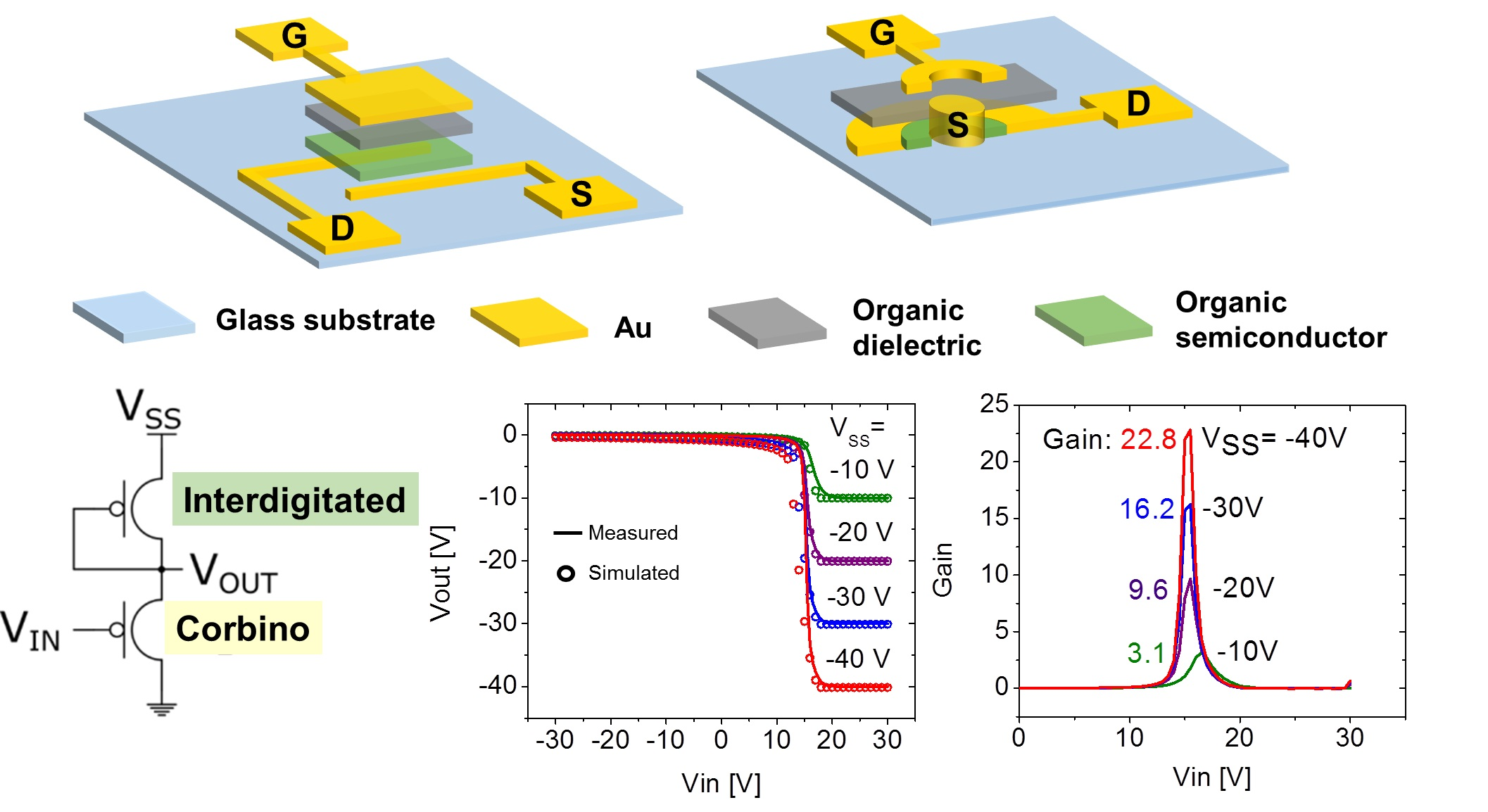
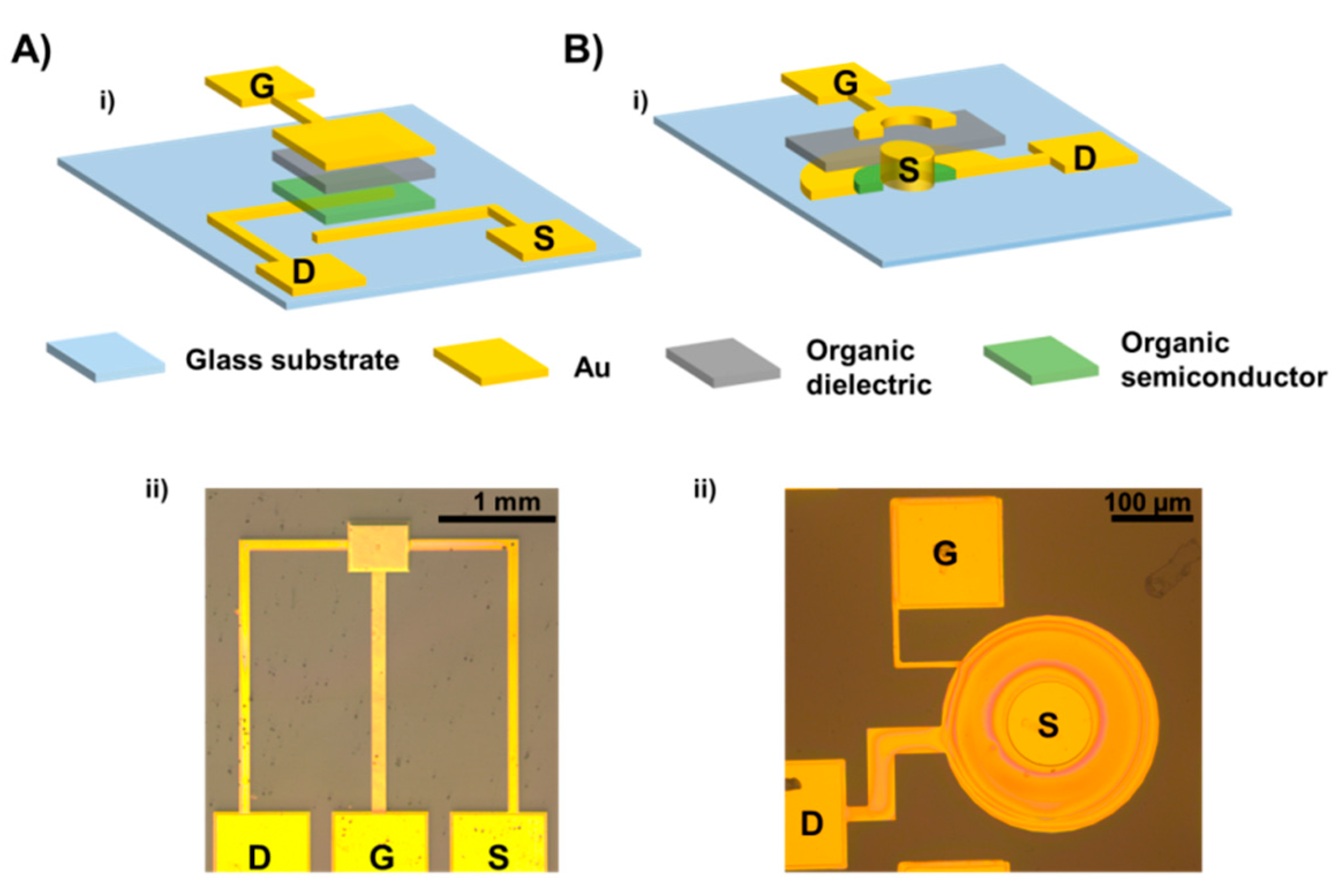
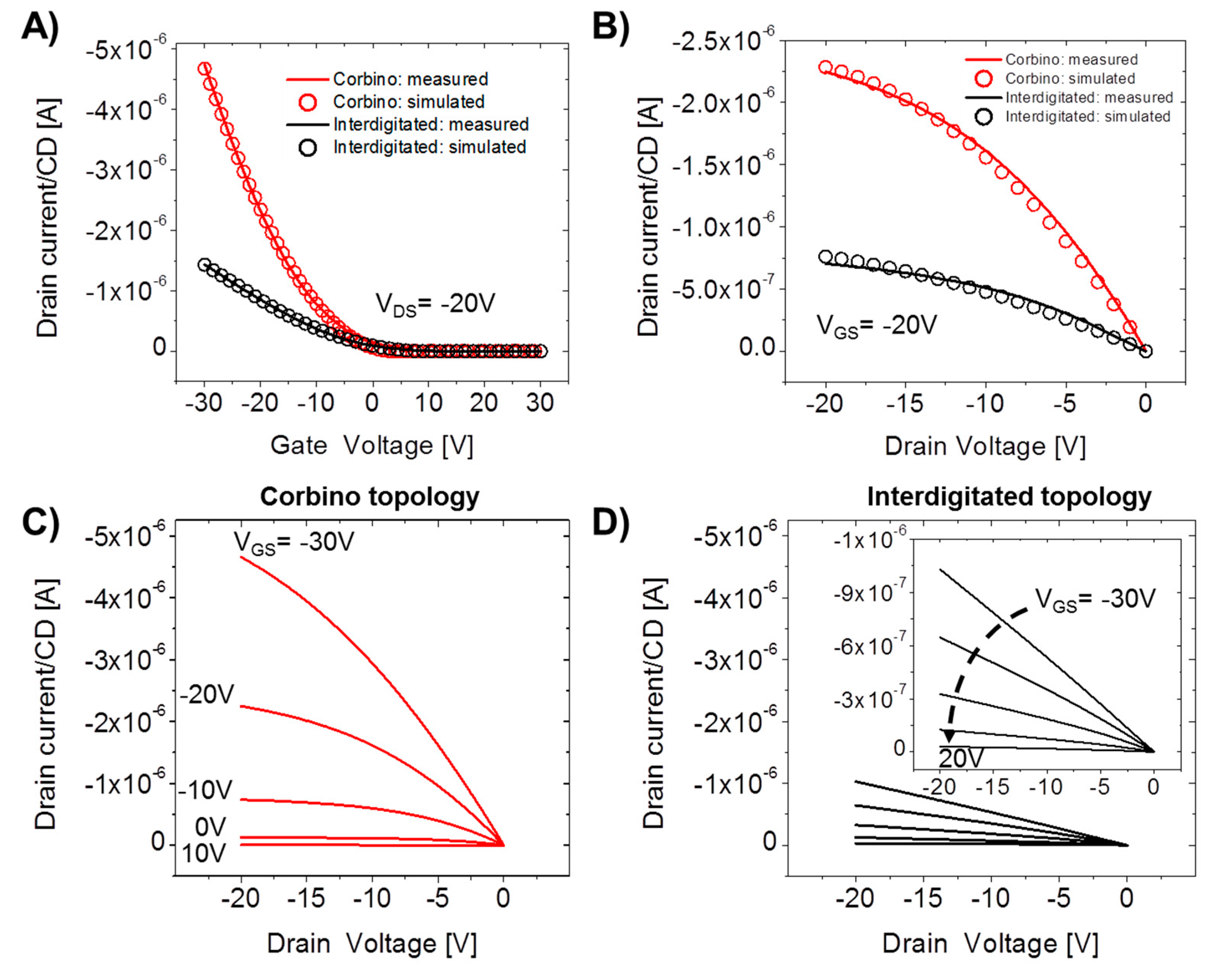
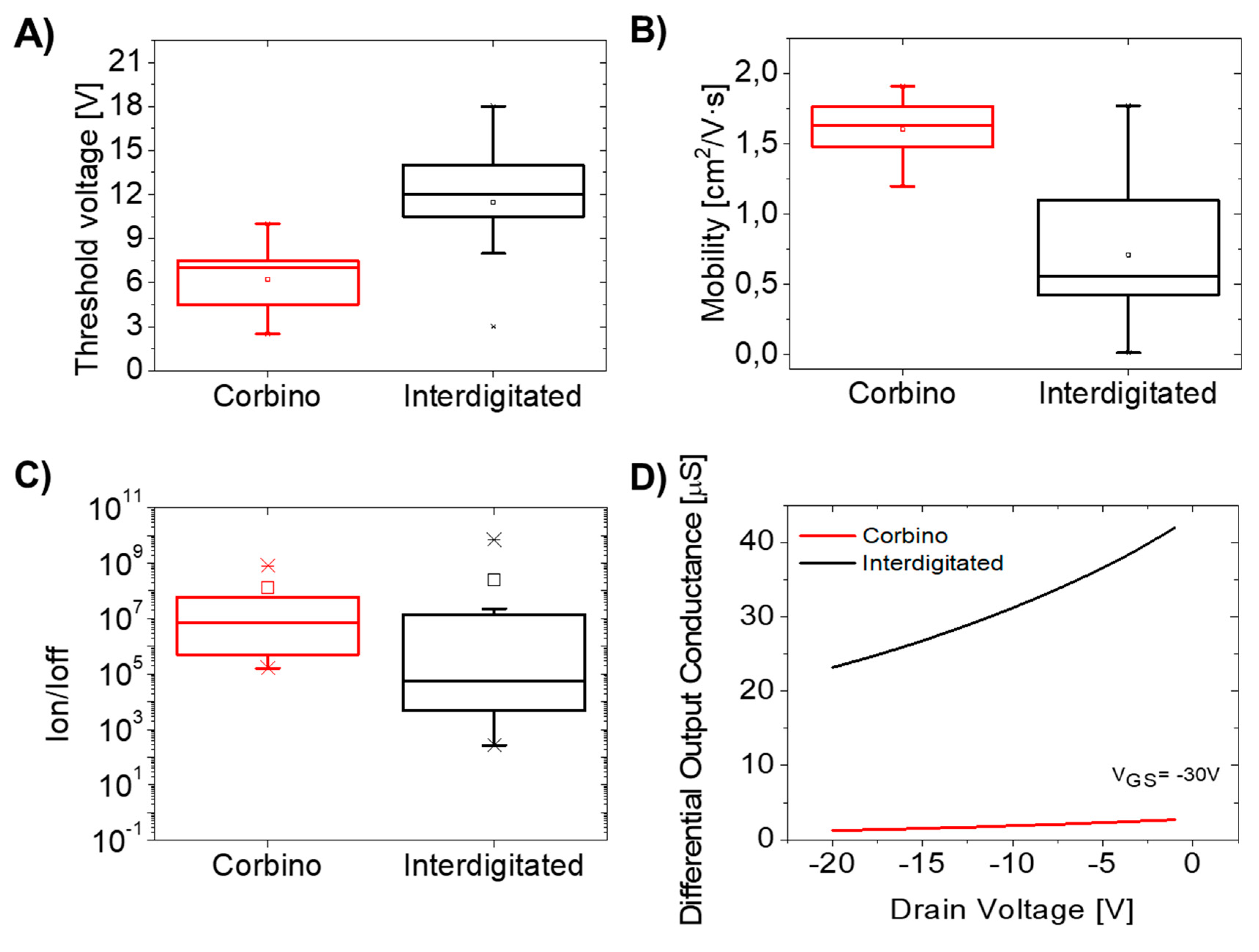
3.1. Interdigitated and Corbino OTFTs

For most of the basic research, the inverted/staggered and co-planar OTFT structures are the most commonly reported devices [39]. OTFTs can be implemented in different structures depending on the relative positions of the electrodes. Moreover, the electrodes in interdigitated configuration were predominantly adapted over the development of OTFT to account for the low conductivity of OSC. In this configuration, the source and drain electrodes are in a form of a comb, such that the finger of the drain comb is interdigitated with the fingers of the source comb providing larger current flow by increasing the channel width. Furthermore, it is worth mentioning that in the interdigitated geometry used in this work the gate layer totally overlies the source and drain electrodes. Figure 1Ai,Aii depicts the scheme and an optical image of the interdigitated electrodes fabricated in this work, respectively. The main advantage of this configuration is their efficiency concerning the ratio between the transistor surface and the transistor width [40]. However, such geometry is not entirely satisfactory in terms of performance since great efforts were made to enhance the alignment of OSC crystal perpendicularly along the Drain and Source (D/S) electrodes during the OSC deposition such as undergoing a nitrogen flow, temperature, and varying the solvent nature and ratio [41,42,43]. In order to overcome this limitation and for the sake of fabrication simplicity, OTFTs with circular channel, called Corbino OTFTs, are commonly proposed. The circular geometry experiences all orientations of the crystals providing less device variability. Although one intrinsic feature of Corbino geometry is a low gate-drain overlying area over their interdigitated geometry counterpart, in this work, the Corbino devices present an overlapped gate-source/drain capacitance of 2.6 × 10⁻⁴ cm2 while the interdigitated devices present 1.4 × 10⁻⁵ cm2. Figure 1Bi,Bii shows a cross-section and the optical image of interdigitated and Corbino geometries, respectively.
Interdigitated and Corbino OTFTs were electrically characterized with a W/L of 40 (W = 160 µm/L = 4 µm) and 34 (W = 680 µm/L = 20 µm), respectively. For a better understanding of the device performances according to the geometry, the transfer curves were compared by normalizing the drain current with the W/L ratio, called channel dimension (CD). Since the devices were fabricated simultaneously on the same substrate, they show the same layer thicknesses and characteristics, thus, the observed differences in the transfer-output electrical characteristics are solely attributed to OTFT geometry.
The measured and simulated transfer and the output characteristics of the interdigitated and Corbino OTFTs are shown in Figure 2. As can be observed in Figure 2A, the model correctly predicts with high precision the transfer curves for both geometries. In addition, the simulated output curves fit well with the measurement by providing a smooth linear-to-saturation transition, as shown in Figure 2B. Thus, the used model can be widely applied to OTFTs with interdigitated and Corbino geometries serving as a practical and versatile tool for organic-based circuit development. Figure 2C,D show the measured output electrical characteristics for both geometries. The maximum drain current, named as ION, is significantly larger for Corbino devices than interdigitated devices, as can be observed in the zoom-in in Figure 2D, presenting values of 4.8 µA and 1.4 µA, respectively, for VDS = −20 V and VGS= −20 V. The same tendency is corroborated in the linear regime as can be seen in the transfer curve in Figure S3, where the higher current is attributed to the Corbino geometry. Despite the fact that effective carrier mobility is affected by the dimensions of the channel length, the Corbino OTFTs tends slightly to saturate. In contrast, the output drain current of interdigitated OTFTs showed a linear increase with VDS and did not saturate. The unsaturated output characteristics in interdigitated devices were also clearly of larger channel length (see Figure S4 Supporting Information), thus, this phenomenon was not totally governed by short-channel effects. Indeed, the output characteristics of both geometries exhibited an obvious IDS offset at VGS = 0 V indicating an appreciable conduction, more pronounced in interdigitated OTFTs, due to a parasitic conduction path from the drain to the source. Due to this fact, the depletion mode current, which is called IOFF, can be achieved by applying a positive voltage such that the conduction is suppressed. The depletion mode current in interdigitated geometry was reached by applying a VGS = −20 V while in Corbino geometry the voltage applied was reduced to VGS = −10 V, as can be compared in Figure 2C and the inset of Figure 2D. The IOFF displayed are about one order of magnitude larger for interdigitated compared with Corbino devices, for VGS = 0 V and VDS = −20 V. In comparison with the Corbino devices reported previously [32], the circular devices developed in this work yielded similar output curves regardless the bias configuration, i.e., the inner-drain or outer-drain condition (see Figure S5, Supporting Information).
In order to gain insight into the electrical performance of both geometries, effective mobility, VT, and ION/IOFF current ratio were investigated as a figure of merit of interdigitated and Corbino geometries as shown in Figure 3A–C, respectively. Notably, there is a big difference in the effective hole mobility between the devices with different geometries. This result is due to the Corbino geometry despite presenting higher channel length compared with interdigitated OTFTs. The extracted effective hole mobility for Corbino geometries is about 1.61 cm2/V·s, and for interdigitated devices is about 0.71 cm2/V·s. Clearly, the OTFTs with Corbino geometry performed VT closer to 0 V in the 4–8 V range, whereas interdigitated geometry performed VT ranging from 8 to 14 V. Despite showing different threshold voltage for each geometry, the turn on voltage is the same for both devices since they share the same materials and fabrication procedure. Turn-on voltage has been extracted from the maximum point of the derivative in the logarithmic scale of the transfer curve and this result is included in Figure S6. Corbino devices present less variability of VON values than the interdigitated geometry devices. Regarding this difference, both types have very similar values for the turn on voltage, which is linked to the materials of the devices. Both devices work in accumulation mode, a result in good agreement with the improvement of the effective hole mobility in Corbino devices, which makes the VT nearer zero. Interestingly, in the Corbino OTFTs, the VT and effective hole mobility possess uniformity in terms of electrical parameter dispersion, which indicates that circular channel geometry is more robust in delivering good performance over large areas despite the polycrystalline nature of the small-molecules. A large number of methods have been developed to reduce the OTFT’s current variability induced by random grain orientations of the organic semiconductor [44,45,46]. The semiconductor used in this work, FlexOSTM, presents large crystal sizes in the range of tens of micrometres. As the grain structures have different grain orientations, the extreme grain-to-channel alignments were solved by a circular-shaped channel providing higher effective mobility and thus, lower VT. The channel length is in the range of the grain domains: L = 4 µm and 20 µm for interdigitated and Corbino geometries, respectively. In order to measure the uniformity of the devices, the relative standard deviation (RSD), defined as the ratio of the standard deviation to the mean drain current, was used. In particular, our results show that the overall RSD in drain current for interdigitated OTFT and Corbino OTFT were found to be 65.18% and 12.4%, respectively. Apart from the reduction in variability, an enhanced effective mobility and threshold voltage were achieved for Corbino OTFTs. Other electrical parameters of the devices have been studied as can be seen in Figure 3C, where the ION/IOFF ratio is degraded for interdigitated devices owing to the presence of parasitic current in the OFF state. The ION/IOFF ratios for Corbino geometries are about (107), two orders of magnitude higher than those of interdigitated devices. For logic gates, the ION/IOFF ratio remains an important parameter that must be taken into account. Thus, a high current modulation ratio is a more important requirement than the high mobility for programmable electronic circuits [43,47,48,49,50]. This behaviour is supported by the fact that Corbino geometry eliminates parasitic sources to drain current flows, hence, allowing an enhanced ION/IOFF ratio. This phenomenon, previously reported in [33], is explained by the increment of the differential output conductance of Corbino devices, which is defined as δIDSVDS and can be described as follows: For circular OTFTs, the W/L relationship remains fairly constant because the channel length modulation is compensated by the channel width modulation. Hence, beyond the pinch-off, the differential output resistance of the interdigitated TFT is finite; whereas, that of the Corbino TFT is infinite, which is in agreement with previous works [31,33] and with the results obtained in Figure 3D.
To conclude, these results reflect the fact that the electrical performances actually correlate with the overall geometric parameter (µhCINSW/L) as supported by the higher the effective hole mobility (µh), the higher the VT and, the higher the ION/IOFF ratios for Corbino geometry. For these reasons, and as a novelty compared with widely-reported logic gates based on interdigitated OTFTs, an inverter logic gate was implemented in further studies in this work.

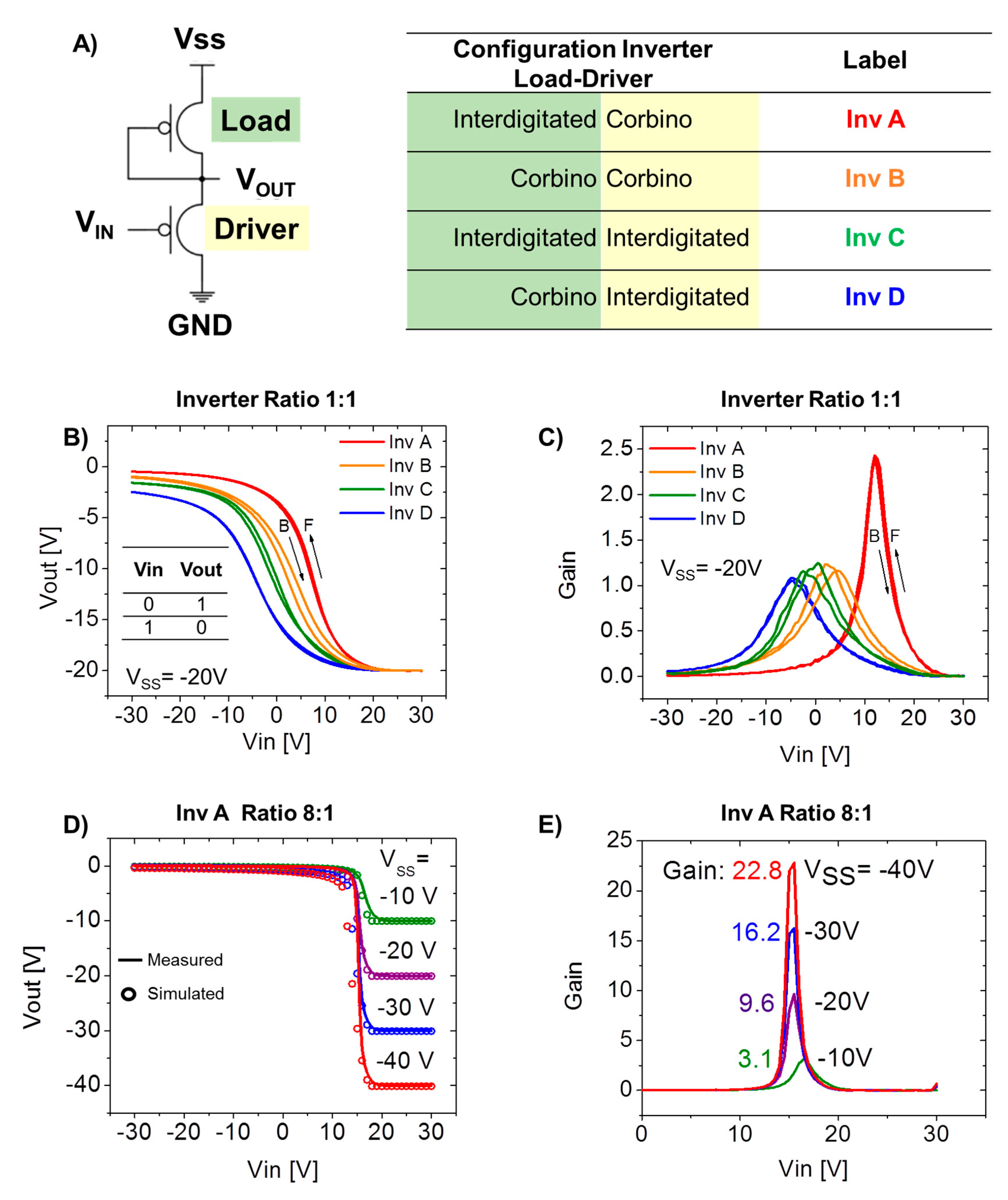
3.2. Unipolar Organic Dual-Geometry Threshold Voltage Inverter

The Inverter is considered to be the most basic logic circuit element for Complementary Metal-Oxide Semiconductor (CMOS) technology [51]. However, unipolar logic circuits are widely employed in the organic electronics field.
Unipolar based circuits which present either n-type or p-type OSC, require a pull-up (n) or pull-down (p) load transistor polarized in ON state and, an input-controlled drive transistor which logically inverts its input [52,53]. Therefore, for a low voltage (in terms of Boolean algebra, it is known as ‘0’) the input produces a high voltage (in terms of Boolean algebra, it is known as ‘1’) at the output, and vice versa [54]. In order to obtain a pull-down load transistor different geometries can be implemented. One of the most common geometries is based on the short-circuit of the gate and drain terminals yielding a fixed gate-to-source voltage, i.e., VGS = 0 V, which turns the load transistor into a diode. In fact, this configuration is referred to as diode-load or depletion-mode load configuration [55,56]. Based on the results of several works [57] which demonstrated that higher gain can be achieved by diode-load topology, this work will consider a diode-load topology for the inverter.
Different inverter topologies have been presented in the literature for monotype systems as shown in Table 1. From the simplest one using only one transistor and a resistor, to a more complex system where multiple devices are required. The most employed inverter topology for CMOS [58] technology involves two complementary transistors, meaning n-channel and p-channel. The advantage of this topology is full swing in the voltage achieved due to the alternative switching between ON and OFF state of the load and driver. Furthermore, this configuration allows a high gain with a significant robustness to the noise margin. The power consumption reaches minimum values because of the negligible power consumption in the static state of the inverter but, as a drawback, the fabrication processes involved are complex. For the monotype devices, the pseudo-CMOS [57,59] approach is the most robust topology since the polarization of the last transistor stage allows them to achieve full swing at the output. Despite this benefit, this topology requires four transistors and more power rails increasing the power consumption, which is detrimental for energy efficiency. In order to reduce the number of transistors and power sources required, the diode-load [60,61,62,63] is used because it operates with two unipolar transistors. However, this topology is less robust and presents non-full swing voltage at the output. Using dual-gate devices, [29,64,65] the diode-load configuration can have improved noise margins since the drive transistor is more robust against noise. The drawback of dual-gate transistors is the requirement of a more complex fabrication process and the inclusion of an additional power rail in the design.
The solution presented in this work is the use of a dual-threshold configuration [66,67] which provides a lower noise margin and higher voltage swing at the output compared to the diode-load and the dual-gate topology, respectively. Dual-threshold technology has been studied for several years and applied to the silicon technology, achieving power consumption reductions [68,69] and increasing the performance of the system in different aspects as delay [68,70], robust designs [71], asynchronous circuits [72], speed improvement [73] or glitch minimization [74]. The interdigitated and Corbino devices developed in this work present different electrical characteristics, such as VT. Taking advantage of this behaviour, a dual-threshold configuration was implemented using these two geometries in order to obtain enhanced performance and reduced power rails. An interesting feature of this approach is the extreme simplicity for fabricating logic gates because the electrical parameters of the transistors are totally dependent of its geometry, allowing a unique manufacturing process for the entire circuit area.
Figure 4A shows the schematic of the inverter. The load transistor is biased to the ON state, which allows the current to flow through itself by providing low resistance and the driver transistor switches between ON and OFF state controlled by the input. A figure of merit of the inverter circuit is the gain, which is defined as the maximum slope of the transfer curve of the system. Regarding gain, four different combinations of the two geometries for the driver and load were configured and characterized. The dimensions ratio, W/L, of the devices were equal (ratio 1:1) to be sure that the results were not influenced by the dimensions, as can be seen in Figure 4B. It can be noted that the configurations with a single type of geometry, i.e., interdigitated-interdigitated or Corbino-Corbino, provide higher hysteresis than the others. The best combination obtained was placing the interdigitated geometry as a load and the Corbino geometry as the driver (called Inv A), where the gain was double the rest of circuit configurations, as shown in Figure 4C. Moreover, this combination geometry offered the full output voltage swing. Taking into account the driver transistor commutating between the ON and OFF states, the Corbino geometry as used as a driver because it provides higher performance than the interdigitated geometry, in terms of the ION/IOFF ratio, allowing high current in the ON state and a negligible current in the OFF mode. Furthermore, the interdigitated transistor working as a load provided lower output resistance and, thus, a lower voltage drop at the output of the system allowing it to reach ground (GND) and VSS values. Additionally, both geometries presented different threshold voltages, which induced a more resistive load device when the driver was in an ON state. These behaviours occurred owing to the lower VSD and resistance in the OFF state of the driver, permitting a full swing of the output voltage thus reducing the hysteresis of the inverter.
To assess the maximum gain obtained by the topology of Inv A, a variation on the ratio of dimensions between the load transistor and the drive transistor was implemented by increasing the driver 8 times with respect to the load, as can be seen in Figure 4D,E. The study of the electrical behaviour of the inverter for four different VSS revealed a link between the power supply and gain. In fact, the increased gain correlated with a higher power supply and at the same time delivered higher swing and higher slope. Moreover, the simulation of electrical behaviour for Inv A depending on the VSS was implemented in Virtuoso and by introducing the generated models of each geometry, as can be observed in Figure 4D. Well-fitting measurements at the transitions were obtained for low VSS, meanwhile the model correctly predicted the VSS and GND values for all VSS. The increment in the ratio between the driver and the load provided almost four times higher gain compared with the previous 1:1 ratio. This configuration presented a gain of 22.8 of the VSS to −40 V, as can be observed in Figure 4E.

4. Discussion

The implementation of inverter circuits in the organic electronics field has been a hot topic in recent years and different configurations have been tested using diverse circuit topologies. Until now, there have been no publications on improved inverter behaviour using two different geometries of transistors. However, as shown in this work improved inverter behaviour was achieved by exploiting the different electrical parameters, i.e., ION/IOFF ratio, effective mobility and threshold voltage of interdigitated and Corbino geometries. In this work the two OTFTs were fabricated by means of the same fabrication process and materials to produce a novel, monotype dual threshold voltage organic inverter with two different transistor geometries for the load and the driver. An experimental comparison of geometries was presented, in which the same dimensions for the driver and inverter load were used in order to corroborate the advantages of the dual threshold technology. The best configuration with maximum gain and lowest hysteresis in the structure was found to be with a Corbino geometry as the driver and an interdigitated geometry as the load. This configuration provided a gain of up to 22.8 with a power supply of −40 V. The achieved gain was higher than most of the inverters presented with monotype systems. Additionally, the transistors were modelled with a modified MOSFET level 3 to improve fitting with the experimental data. Finally, the models were employed to simulate a circuit of the inverter and a good fit was achieved with the experimental data.

Supplementary Materials

The following are available online at https://www.mdpi.com/2073-4352/9/7/333/s1, Figure S1: Molecule structures of the small molecule organic semiconductor and the high-k polymer semiconductor binder used for the blend. Figure S2: Square root and logarithmic scale transfer curves of both geometries types for the two behavior of the transistors: (a) Lineal region, and (b) saturation region including the threshold voltage extraction procedure representation. Figure S3: Experimental transfer characteristics for Corbino and interdigitated geometries normalized to channel dimension (CD) for VDS = −2 V. Figure S4: Experimental output characteristics of interdigitated geometry devices where gate voltage (VGS) were swept by −10 V from −30 V to 10 V. The channel length is 10 µm. Figure S5: Output characteristics of the Corbino TFT for the two drain-bias conditions: (a) The inner circle as source and outer ring as drain; and (b) the inner circle as drain and outer ring as source. Figure S6: Turn on voltage of both geometries from the curve transfer curve with VDS = −20 V. The central mark represents the median, box limits indicate the 25th and 75th percentiles, and whiskers extend to 5th and 9th percentiles.

Author Contributions

Device characterization, model development, circuit simulation and writing—original draft preparation: A.A.; Methodology, formal analysis and writing—review and editing: C.M.-D.; OTFT manufacturing: S.O.; funding acquisition and project administration: L.T. Conceptualization and supervision: E.R.

Funding

This research was funded by MICIU-Spain, grant number RTI2018–102070-B-C21.

Acknowledgments

The authors would like to thank Neudrive, Ltd. (UK) for providing the OTFT samples used on this work.

Conflicts of Interest

The authors declare no conflict of interest.

References

  1. Tang, W.; Huang, Y.; Han, L.; Liu, R.; Su, Y.; Guo, X.; Yan, F. Recent progress in printable organic field effect transistors. J. Mater. Chem. C 2019, 7, 790–808. [Google Scholar] [CrossRef]
  2. Sirringhaus, H. 25th anniversary article: Organic field-effect transistors: The path beyond amorphous silicon. Adv. Mater. 2014, 26, 1319–1335. [Google Scholar] [CrossRef] [PubMed]
  3. Chang, J.S.; Facchetti, A.F.; Reuss, R.; Member, S.; Facchetti, A.F.; Reuss, R. A Circuits and Systems Perspective of Organic/Printed Electronics: Review, Challenges, and Contemporary and Emerging Design Approaches. IEEE J. Emerg. Sel. Top. Circuits Syst. 2017, 7, 7–26. [Google Scholar] [CrossRef]
  4. Gamota, D.R. Printed organic and molecular electronics. Mater. Today 2004, 7, 53. [Google Scholar]
  5. Ling, M.M.; Bao, Z. Thin film deposition, patterning, and printing in organic thin film transistors. Chem. Mater. 2004, 16, 4824–4840. [Google Scholar] [CrossRef]
  6. Chabinyc, M.L.; Salleo, A. Materials requirements and fabrication of active matrix arrays of organic thin-film transistors for displays. Chem. Mater. 2004, 16, 4509–4521. [Google Scholar] [CrossRef]
  7. Chou, W.Y.; Kuo, C.W.; Cheng, H.L.; Chen, Y.R.; Tang, F.C.; Yang, F.Y.; Shu, D.Y.; Liao, C.C. Effect of surface free energy in gate dielectric in pentacene thin-film transistors. Appl. Phys. Lett. 2006, 89, 2004–2007. [Google Scholar] [CrossRef]
  8. Forrest, S.R. The path to ubiquitous and low-cost organic electronic appliances on plastic. Nature 2014, 428, 911–918. [Google Scholar] [CrossRef]
  9. Anthopoulos, T.D.; De Leeuw, D.M.; Cantatore, E.; Setayesh, S.; Meijer, E.J.; Tanase, C.; Hummelen, J.C.; Blom, P.W.M. Organic complementary-like inverters employing methanofullerene-based ambipolar field-effect transistors. Appl. Phys. Lett. 2004, 85, 4205–4207. [Google Scholar] [CrossRef] [Green Version]
  10. Meijer, E.J.; De Leeuw, D.M.; Setayesh, S.; Van Veenendaal, E.; Huisman, B.H.; Blom, P.W.M.; Hummelen, J.C.; Scherf, U.; Klapwijk, T.M. Solution-processed ambipolar organic field-effect transistors and inverters. Nat. Mater. 2003, 2, 678–682. [Google Scholar] [CrossRef]
  11. Yoneya, N.; Ono, H.; Ishii, Y.; Himori, K.; Hirai, N.; Abe, H.; Yumoto, A.; Kobayashi, N.; Nomoto, K. Flexible electrophoretic display driven by solution-processed organic thin-film transistors. J. Soc. Inf. Disp. 2012, 20, 143. [Google Scholar] [CrossRef]
  12. Myny, K.; Steudel, S.; Vicca, P.; Beenhakkers, M.J.; van Aerle, N.A.J.M.; Gelinck, G.H.; Genoe, J.; Dehaene, W.; Heremans, P. Plastic circuits and tags for 13.56 MHz radio-frequency communication. Solid. State. Electron. 2009, 53, 1220–1226. [Google Scholar] [CrossRef]
  13. Cao, Q.; Kim, H.S.; Pimparkar, N.; Kulkarni, J.P.; Wang, C.; Shim, M.; Roy, K.; Alam, M.A.; Rogers, J.A. Medium-scale carbon nanotube thin-film integrated circuits on flexible plastic substrates. Nature 2008, 454, 495–500. [Google Scholar] [CrossRef]
  14. Fluxman, S.M. Design and performance of digital polysilicon thin-film-transistor circuits on glass. IEE Proc. Circuits, Devices Syst. 1994, 141, 56. [Google Scholar] [CrossRef]
  15. Bae, B.S.; Choi, J.W.; Oh, J.H.; Jang, J. Level shifter embedded in drive circuits with amorphous silicon TFTs. IEEE Trans. Electron Devices 2006, 53, 494–498. [Google Scholar]
  16. Greening, B.; Kuo, C.C.; Sheraw, C.D.; Gundlach, D.J.; Cuomo, F.P.; Klauk, H.; Campi, J.; Nichols, J.A.; Huang, J.R.; Jia, L.; et al. Analog and digital circuits using organic thin-film transistors on polyester substrates. IEEE Electron Device Lett. 2000, 21, 534–536. [Google Scholar]
  17. Fuketa, H.; Yoshioka, K.; Shinozuka, Y.; Ishida, K.; Yokota, T.; Matsuhisa, N.; Inoue, Y.; Sekino, M.; Sekitani, T.; Takamiya, M.; et al. 1 µm-Thickness Ultra-Flexible and High Electrode-Density Surface Electromyogram Measurement Sheet With 2 V Organic Transistors for Prosthetic Hand Control. IEEE Trans. Biomed. Circuits Syst. 2014, 8, 824–833. [Google Scholar] [CrossRef]
  18. Ishida, K.; Huang, T.C.; Honda, K.; Sekitani, T.; Nakajima, H.; Maeda, H.; Takamiya, M.; Someya, T.; Sakurai, T. A 100-V AC energy meter integrating 20-V organic CMOS digital and analog circuits with a floating gate for process variation compensation and a 100-V organic pMOS rectifier. IEEE J. Solid-State Circuits 2012, 47, 301–309. [Google Scholar] [CrossRef]
  19. Feng, L.; Tang, W.; Zhao, J.; Cui, Q.; Jiang, C.; Guo, X. All-solution-processed low-voltage organic thin-film transistor inverter on plastic substrate. IEEE Trans. Electron Devices 2014, 61, 1175–1180. [Google Scholar] [CrossRef]
  20. Myny, K.; Beenhakkers, M.; van Aerle, N.; Gelinck, G.; Genoe, J.; Dehaene, W.; Heremans, P. Unipolar organic transistor circuits made robust by dual-gate technology. IEEE J. Solid-State Circuits 2011, 46, 1223–1230. [Google Scholar] [CrossRef]
  21. Kergoat, L.; Herlogsson, L.; Piro, B.; Pham, M.C.; Horowitz, G.; Crispin, X.; Berggren, M. Tuning the threshold voltage in electrolyte-gated organic field-effect transistors. Proc. Natl. Acad. Sci. USA 2012, 109, 8394–8399. [Google Scholar] [CrossRef] [PubMed] [Green Version]
  22. Hoon Kim, S.; Rim Hwang, H.; Joong Kwon, H.; Jang, J. Unipolar depletion-load organic circuits on flexible substrate by self-organized polymer blending with 6, 13-bis (triisopropylsilylethynyl) pentacene using ink-jet printing. Appl. Phys. Lett. 2012, 100, 053302. [Google Scholar] [CrossRef]
  23. Pernstich, K.P.; Haas, S.; Oberhoff, D.; Goldmann, C.; Gundlach, D.J.; Batlogg, B.; Rashid, A.N.; Schitter, G. Threshold voltage shift in organic field effect transistors by dipole monolayers on the gate insulator. J. Appl. Phys. 2004, 96, 6431–6438. [Google Scholar] [CrossRef] [Green Version]
  24. Kobayashi, S.; Nishikawa, T.; Takenobu, T.; Mori, S.; Shimoda, T.; Mitani, T.; Shimotani, H.; Yoshimoto, N.; Ogawa, S.; Iwasa, Y. Control of carrier density by self-assembled monolayers in organic field-effect transistors. Nat. Mater. 2004, 3, 317–322. [Google Scholar] [CrossRef] [PubMed]
  25. Choi, J.M.; Im, S. Optimum channel thickness of rubrene thin-film transistors. Appl. Phys. Lett. 2008, 93, 2006–2009. [Google Scholar] [CrossRef]
  26. Wang, A.; Kymissis, I.; Bulović, V.; Akinwande, A.I. Tunable threshold voltage and flatband voltage in pentacene field effect transistors. Appl. Phys. Lett. 2006, 89, 112109. [Google Scholar] [CrossRef]
  27. Wang, A.; Kymissis, I.; Bulović, V.; Akinwande, A.I. Engineering density of semiconductor-dielectric interface states to modulate threshold voltage in OFETs. IEEE Trans. Electron Devices 2006, 53, 9–13. [Google Scholar] [CrossRef]
  28. Takamiya, M.; Sekitani, T.; Kato, Y.; Kawaguchi, H.; Someya, T.; Sakurai, T. An Organic FET SRAM for Braille Sheet Display with Back Gate to Increase Static Noise Margin. 2006 IEEE Int. Solid State Circuits Conf.-Dig. Tech. Pap. 2006, 42, 1060–1069. [Google Scholar]
  29. Koo, J.B.; Ku, C.H.; Lim, J.W.; Kim, S.H. Novel organic inverters with dual-gate pentacene thin-film transistor. Org. Electron. 2007, 8, 552–558. [Google Scholar] [CrossRef]
  30. Ogier, S.D.; Matsui, H.; Feng, L.; Simms, M.; Mashayekhi, M.; Carrabina, J.; Terés, L.; Tokito, S. Uniform, high performance, solution processed organic thin-film transistors integrated in 1 MHz frequency ring oscillators. Org. Electron. 2018, 54, 40–47. [Google Scholar] [CrossRef]
  31. Mativenga, M.; Choe, Y.; Um, J.; Jang, J. Corbino Oxide TFTs for Flexible AMOLED Display Stability; Wiley Publishing: San Francisco, CA, USA, 2016; pp. 1147–1150. [Google Scholar]
  32. Lee, H.; Yoo, J.S.; Kim, C.D.; Chung, I.J.; Kanicki, J. Asymmetric electrical properties of Corbino a-Si:H TFT and concepts of its application to flat panel displays. IEEE Trans. Electron Devices 2007, 54, 654–662. [Google Scholar] [CrossRef]
  33. Mativenga, M.; Ha, S.H.; Geng, D.; Kang, D.H.; Mruthyunjaya, R.K.; Heiler, G.N.; Tredwell, T.J.; Jang, J. Infinite output resistance of corbino thin-film transistors with an amorphous-InGaZnO active layer for large-area AMOLED displays. IEEE Trans. Electron Devices 2014, 61, 3199–3205. [Google Scholar] [CrossRef]
  34. Chen, J.; Tee, C.K.; Shtein, M.; Anthony, J.; Martin, D.C. Grain-boundary-limited charge transport in solution-processed 6,13 bis (tri-isopropylsilylethynyl) pentacene thin film transistors. J. Appl. Phys. 2008, 103, 114513. [Google Scholar] [CrossRef]
  35. Steiner, F.; Poelking, C.; Niedzialek, D.; Andrienko, D.; Nelson, J. Influence of orientation mismatch on charge transport across grain boundaries in tri-isopropylsilylethynyl (TIPS) pentacene thin films. Phys. Chem. Chem. Phys. 2017, 19, 10854–10862. [Google Scholar] [CrossRef] [PubMed] [Green Version]
  36. Fayez, M.; Morsy, K.; Sabry, M. Simulation of Organic Thin Film Transistor at both Device and Circuit Levels. Int. Conf. Aerosp. Sci. Aviat. Technol. 2019, 16, 1–6. [Google Scholar] [CrossRef]
  37. Dobrescu, L.; Petrov, M.; Dobrescu, D.; Ravariu, C. Threshold voltage extraction methods for MOS transistors. In Proceedings of the 2000 International Semiconductor Conference, Sinaia, Romania, 10–14 October 2000; pp. 371–374. [Google Scholar]
  38. Munteanu, D.; Cristoloveanu, S.; Hovel, H. Circular Pseudo-Metal Oxide Semiconductor Field Effect Transistor in Silicon-on-Insulator Analytical Model, Simulation, and Measurements. Electrochem. Solid-State Lett. 1999, 2, 242–243. [Google Scholar] [CrossRef]
  39. Guo, X.; Xu, Y.; Ogier, S.; Ng, T.N.; Caironi, M.; Perinot, A.; Li, L.; Zhao, J.; Tang, W.; Sporea, R.A.; et al. Current Status and Opportunities of Organic Thin-Film Transistor Technologies. IEEE Trans. Electron Devices 2017, 64, 1906–1921. [Google Scholar] [CrossRef] [Green Version]
  40. Mashayekhi, M. Inkjet-Configurable Gate Arrays. Towards Application Specific Printed Electronic Circuits. Available online: https://www.tesisenred.net/bitstream/handle/10803/402272/moma1de1.pdf?sequence=1&isAllowed=y (accessed on 27 June 2019).
  41. Fujisaki, Y.; Takahashi, D.; Nakajima, Y.; Nakata, M.; Tsuji, H.; Yamamoto, T. Alignment Control of Patterned Organic Semiconductor Crystals in Short-Channel Transistor Using Unidirectional Solvent Evaporation Process. IEEE Trans. Electron Devices 2015, 62, 2306–2312. [Google Scholar] [CrossRef]
  42. Bi, S.; He, Z.; Chen, J.; Li, D. Solution-grown small-molecule organic semiconductor with enhanced crystal alignment and areal coverage for organic thin film transistors. AIP Adv. 2015, 5, 077170. [Google Scholar] [CrossRef] [Green Version]
  43. Tisserant, J.N.; Wicht, G.; Göbel, O.F.; Bocek, E.; Bona, G.L.; Geiger, T.; Hany, R.; Mezzenga, R.; Partel, S.; Schmid, P.; et al. Growth and alignment of thin film organic single crystals from dewetting patterns. ACS Nano 2013, 7, 5506–5513. [Google Scholar] [CrossRef]
  44. Goto, O.; Tomiya, S.; Murakami, Y.; Shinozaki, A.; Toda, A.; Kasahara, J.; Hobara, D. Organic single-crystal arrays from solution-phase growth using micropattern with nucleation control region. Adv. Mater. 2012, 24, 1117–1122. [Google Scholar] [CrossRef] [PubMed]
  45. Liu, Y.; Zhao, X.; Cai, B.; Pei, T.; Tong, Y.; Tang, Q.; Liu, Y. Controllable fabrication of oriented micro/nanowire arrays of dibenzo-tetrathiafulvalene by a multiple drop-casting method. Nanoscale 2014, 6, 1323–1328. [Google Scholar] [CrossRef] [PubMed]
  46. Li, Y.; Ji, D.; Liu, J.; Yao, Y.; Fu, X.; Zhu, W.; Xu, C.; Dong, H.; Li, J.; Hu, W. Quick Fabrication of Large-area Organic Semiconductor Single Crystal Arrays with a Rapid Annealing Self-Solution-Shearing Method. Sci. Rep. 2015, 5, 1–9. [Google Scholar] [CrossRef] [PubMed]
  47. Sou, A.; Jung, S.; Gili, E.; Pecunia, V.; Joimel, J.; Fichet, G.; Sirringhaus, H. Programmable logic circuits for functional integrated smart plastic systems. Org. Electron. 2014, 15, 3111–3119. [Google Scholar] [CrossRef] [Green Version]
  48. Xu, W.; Liu, Z.; Zhao, J.; Xu, W.; Gu, W.; Zhang, X.; Qian, L.; Cui, Z. Flexible logic circuits based on top-gate thin film transistors with printed semiconductor carbon nanotubes and top electrodes. Nanoscale 2014, 6, 14891–14897. [Google Scholar] [CrossRef] [PubMed]
  49. Sirringhaus, H.; Friend, R.H.; Li, X.C.; Moratti, S.C.; Holmes, A.B.; Feeder, N. Bis(dithienothiophene) organic field-effect transistors with a high ON/OFF ratio. Appl. Phys. Lett. 1997, 71, 3871–3873. [Google Scholar] [CrossRef]
  50. Chandar Shekar, B.; Lee, J.; Rhee, S.W. Organic thin film transistors: Materials, processes and devices. Korean J. Chem. Eng. 2007, 21, 267–285. [Google Scholar] [CrossRef]
  51. Briseno, A.L.; Tseng, R.J.; Li, S.H.; Chu, C.W.; Yang, Y.; Falcao, E.H.L.; Wudl, F.; Ling, M.M.; Chen, H.Z.; Bao, Z.; et al. Organic single-crystal complementary inverter. Appl. Phys. Lett. 2006, 89, 1–4. [Google Scholar] [CrossRef]
  52. Wu, Q.; Zhang, J.Y.; Qin, R.Q. Design Considerations for Digital Circuits Using Organic Thin Film Transistors on a Flexible Substrate. In Proceedings of the 2006 IEEE International Symposium on Circuits and Systems, Island of Kos, Greece, 21–24 May 2006; Volume 1, pp. 1267–1270. [Google Scholar]
  53. Lugli, P.; Csaba, G.; Erlen, C. Modeling of circuits and architectures for molecular electronics. J. Comput. Electron. 2009, 8, 410–426. [Google Scholar] [CrossRef]
  54. Krumm, J. CIRCUIT ANALYSIS METHODOLOGY FOR ORGANIC TRANSISTORS. Available online: https://opus4.kobv.de/opus4-fau/files/627/diss.pdf (accessed on 27 June 2019).
  55. Lee, C.A.; Jin, S.H.; Jung, K.D.; Lee, J.D.; Park, B.G. Full-swing pentacene organic inverter with enhancement-mode driver and depletion-mode load. Solid. State. Electron. 2006, 50, 1216–1218. [Google Scholar] [CrossRef]
  56. Brown, A.R.; De Leeuw, D.M.; Havinga, E.E.; Pomp, A. Field-effect transistors made from solution-processed organic semiconductors. Synth. Met. 1994, 68, 65–70. [Google Scholar] [CrossRef]
  57. Huang, T.C.; Fukuda, K.; Lo, C.M.; Yeh, Y.H.; Sekitani, T.; Someya, T.; Cheng, K.T. Pseudo-CMOS: A design style for low-cost and robust flexible electronics. IEEE Trans. Electron Devices 2011, 58, 141–150. [Google Scholar] [CrossRef]
  58. Zeng, W.J.; Zhou, X.Y.; Pan, X.J.; Song, C.L.; Zhang, H.L. High performance CMOS-like inverter based on an ambipolar organic semiconductor and low cost metals. AIP Adv. 2013, 3, 012101. [Google Scholar] [CrossRef] [Green Version]
  59. Fukuda, K.; Sekitani, T.; Yokota, T.; Kuribara, K.; Huang, T.C.; Sakurai, T.; Zschieschang, U.; Klauk, H.; Ikeda, M.; Kuwabara, H.; et al. Organic pseudo-CMOS circuits for low-voltage large-gain high-speed operation. IEEE Electron Device Lett. 2011, 32, 1448–1450. [Google Scholar] [CrossRef]
  60. Kim, S.H.; Jang, J.; Jeon, H.; Yun, W.M.; Nam, S.; Park, C.E. Hysteresis-free pentacene field-effect transistors and inverters containing poly (4-vinyl phenol-co-methyl methacrylate) gate dielectrics. Appl. Phys. Lett. 2008, 92, 1–4. [Google Scholar] [CrossRef]
  61. Kim, S.H.; Choi, D.; Chung, D.S.; Yang, C.; Jang, J.; Park, C.E.; Park, S.H.K. High-performance solution-processed triisopropylsilylethynyl pentacene transistors and inverters fabricated by using the selective self-organization technique. Appl. Phys. Lett. 2008, 93, 1–4. [Google Scholar] [CrossRef]
  62. Koo, J.B.; Ku, C.H.; Lim, S.C.; Kim, S.H.; Lee, J.H. Hysteresis and threshold voltage shift of pentacene thin-film transistors and inverters with Al2O3 gate dielectric. Appl. Phys. Lett. 2007, 90, 1–4. [Google Scholar] [CrossRef]
  63. Park, S.K.; Member, S.; Anthony, J.E.; Jackson, T.N. Solution-Processed TIPS-Pentacene Organic Thin-Film-Transistor Circuits. IEEE Electron Device Lett. 2007, 28, 2007–2009. [Google Scholar] [CrossRef]
  64. Myny, K.; Beenhakkers, M.; van Aerle, N.; Gelinck, G.; Genoe, J.; Dehaene, W.; Heremans, P. Robust digital design in organic electronics by dual-gate technology. IEEE Int. Solid-State Circuits Conf. Dig. Tech. Pap. 2010, 8, 140–141. [Google Scholar]
  65. Spijkman, M.J.; Myny, K.; Smits, E.C.P.; Heremans, P.; Blom, P.W.M.; De Leeuw, D.M. Dual-gate thin-film transistors, integrated circuits and sensors. Adv. Mater. 2011, 23, 3231–3242. [Google Scholar] [CrossRef]
  66. Nausieda, I.; Ryu, K.K.; He, D.D.; Akinwande, A.I.; Bulovic, V.; Sodini, C.G. Mixed-signal organic integrated circuits in a fully photolithographic dual threshold voltage technology. IEEE Trans. Electron Devices 2011, 58, 865–873. [Google Scholar] [CrossRef]
  67. Nausieda, I.; Ryu, K.K.; He, D.D.; Akinwande, A.I.; Bulović, V.; Sodini, C.G. Dual threshold voltage organic thin-film transistor technology. IEEE Trans. Electron Devices 2010, 57, 3027–3032. [Google Scholar] [CrossRef]
  68. Wei, L.; Chen, Z.; Johnson, M.; Roy, K.; De, V. Design and optimization of low voltage high performance dual threshold CMOS circuits. In Proceedings of the 35th annual Design Automation Conference, San Francisco, CA, USA, 15–19 June 1998; pp. 489–494. [Google Scholar]
  69. Sundararajan, V.; Parhi, K.K. Low power synthesis of dual threshold voltage CMOS VLSI circuits. In Proceedings of the 1999 International Symposium on Low Power Electronics and Design, San Diego, CA, USA, 17 August 1999; pp. 139–144. [Google Scholar]
  70. Ghosh, A.; Ghosh, D. Optimization of static power, leakage power and delay of full adder circuit using dual threshold MOSFET based design and T-spice simulation. In Proceedings of the 2009 International Conference on Advances in Recent Technologies in Communication and Computing, Kerala, India, 27–28 October 2009; pp. 903–905. [Google Scholar]
  71. Islam, A.; Akram, M.W.; Pable, S.D.; Hasan, M. Design and analysis of robust dual threshold CMOS full adder circuit in 32nm technology. In Proceedings of the 2010 International Conference on Advances in Recent Technologies in Communication and Computing, Kottayam, India, 16–17 October 2010; pp. 418–420. [Google Scholar]
  72. Ghavami, B.; Pedram, H. Design of dual threshold voltages asynchronous circuits. In Proceedings of the 2008 international symposium on Low Power Electronics & Design, Bangalore, India, 11–13 August 2008; p. 185. [Google Scholar]
  73. Wang, C.; Huang, C.; Lee, C. A Low Power High-Speed 8-Bit Pipelining CLA Design Using Dual-Threshold Voltage Domino Logic. IEEE Trans. Very Large Scale Integr. VLSI Syst. 2008, 16, 594–598. [Google Scholar] [CrossRef] [Green Version]
  74. Slimani, M.; Matherat, P.; Mathieu, Y. A dual threshold voltage technique for glitch minimization. In Proceedings of the 2012 19th IEEE International Conference on Electronics, Circuits, and Systems (ICECS 2012), Seville, Spain, 9–12 December 2012; pp. 444–447. [Google Scholar]
Figure 1. (A) (i) 3D scheme of the Interdigitated geometry and (ii) its optical image; (B) (i) 3D scheme of the Corbino geometry and (ii) its optical image. D, G and S refer to drain, gate and source electrodes, respectively.
Crystals 09 00333 g001
Figure 2. Experimental transfer (A) and output (B) characteristics for Corbino and interdigitated geometries normalized to Channel Dimension (CD) for VDS = −20 V and VGS = −20 V, respectively. The circular symbol refers to the theoretical transfer and output characteristics simulated by using a MOSFET level 3. (C) Experimental output characteristics of Corbino geometry devices. (D) Experimental output characteristics of interdigitated geometry devices where gate voltage (VGS) were swept by −10 V from −30 V to 20 V. The output graph for interdigitated geometry is rescaled in the inset graph for better comparison. The channel length is 4 µm and 20 µm for interdigitated and the Corbino devices, respectively. Both have almost the same W/L ratio.
Crystals 09 00333 g002
Figure 3. Electrical parameters such as (A) threshold voltage, (B) effective hole mobility and (C) ION/IOFF ratio for Corbino and interdigitated geometries. The central mark represents the median, box limits indicate the 25th and 75th percentiles, and whiskers extend to the 5th and 9th percentiles. (D) Differential output conductance as a function of drain voltage at VGS = −30 V.
Crystals 09 00333 g003
Figure 4. (A) Inverter circuits by using different combinations of transistor geometries: (B) Voltage transfer characteristics (VTC); (C) and gain. (D) VTC for Inv A geometry with a ratio 8:1; and (E) the respective gain. ”F” and “B” denote forward and backward sweeps, respectively.
Crystals 09 00333 g004
Table 1. Comparison of different topologies of OTFT design styles for basic inverters with key parameters.
Inverter TopologiesCMOS
Crystals 09 00333 i001
Pseudo-CMOS
Crystals 09 00333 i002
Dual-Gate
Crystals 09 00333 i003
Diode-Load
Crystals 09 00333 i004
Dual-Threshold
Crystals 09 00333 i005
Transistors24222
Power rails23322
Noise MarginMost RobustHigh RobustRobustPoor RobustMedium Robust
Voltage swingFull SwingFull SwingNon-Full SwingNon-Full SwingAlmost-Full Swing
PowerDynamicStatic and DynamicStatic and DynamicStatic and DynamicStatic and Dynamic
Device TypeComplementary typeMono-typeMono-typeMono-typeMono-type

