Effects of Sm2O3 and V2O5 Film Stacking on Switching Behaviors of Resistive Random Access Memories


Abstract
:1. Introduction
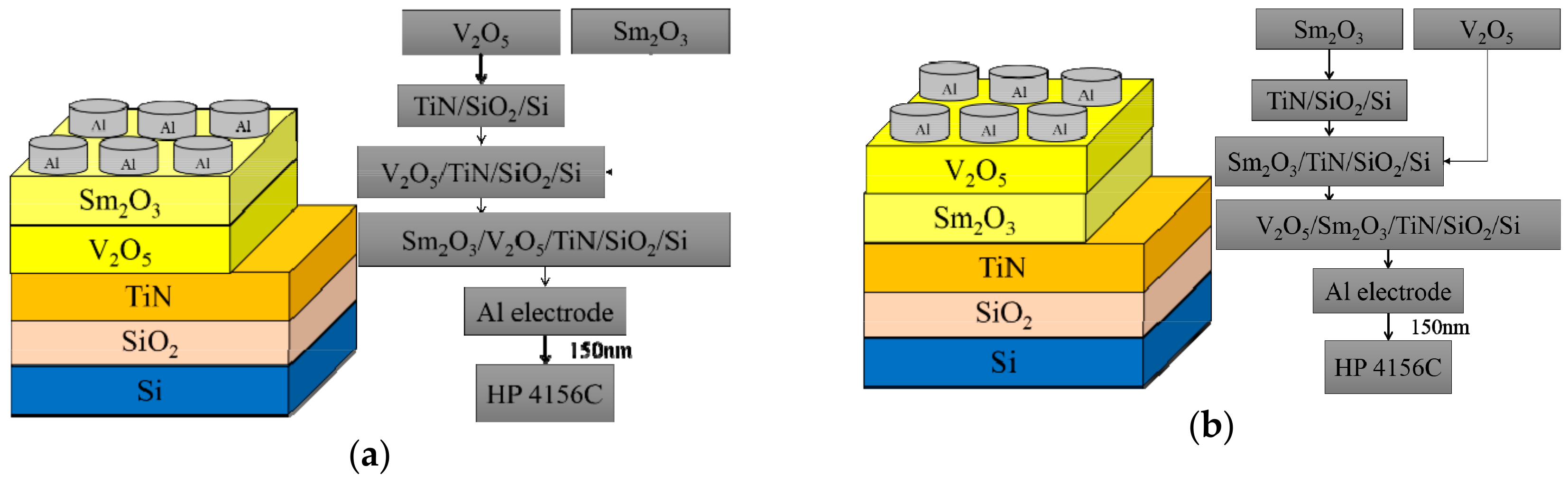
2. Experimental
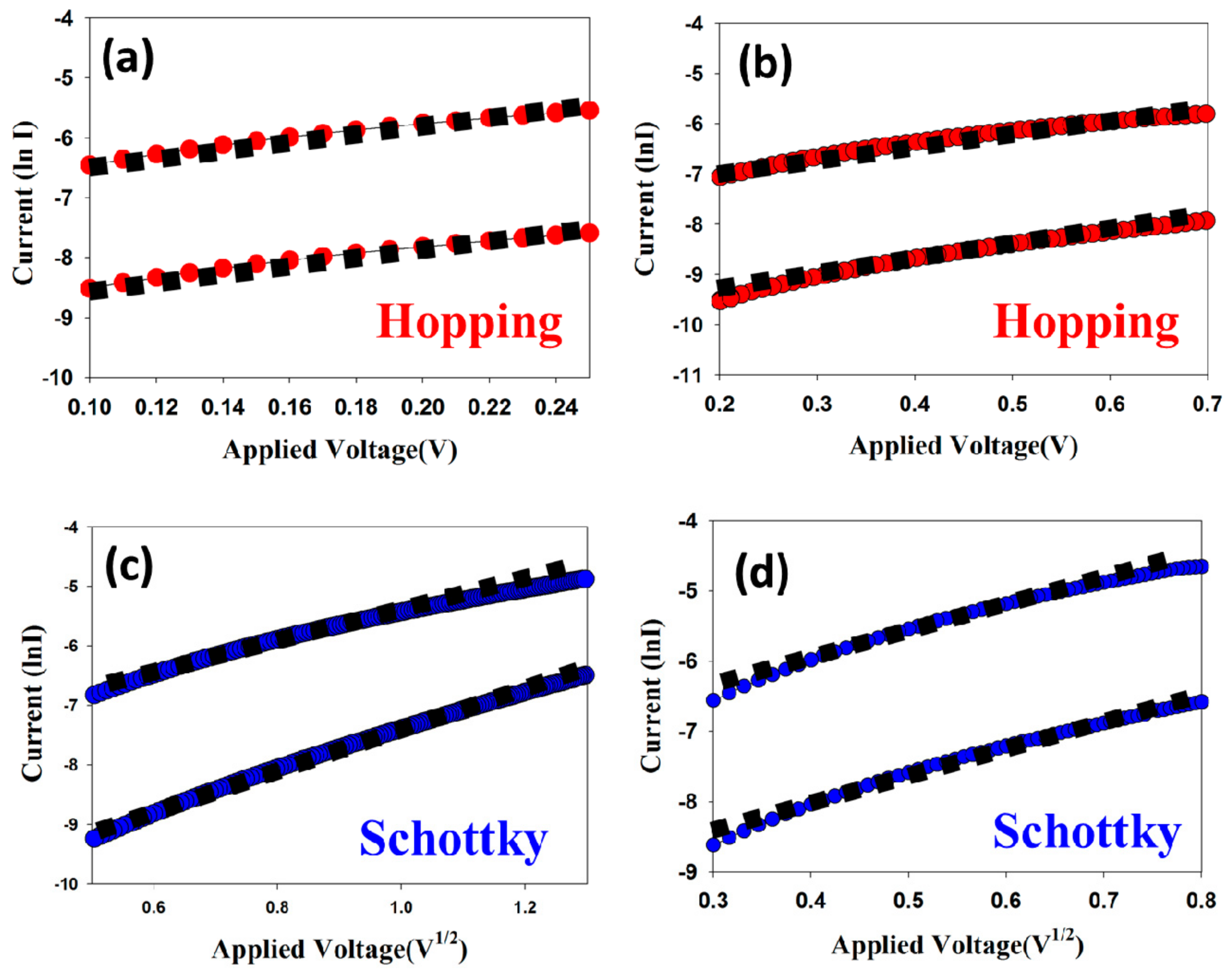
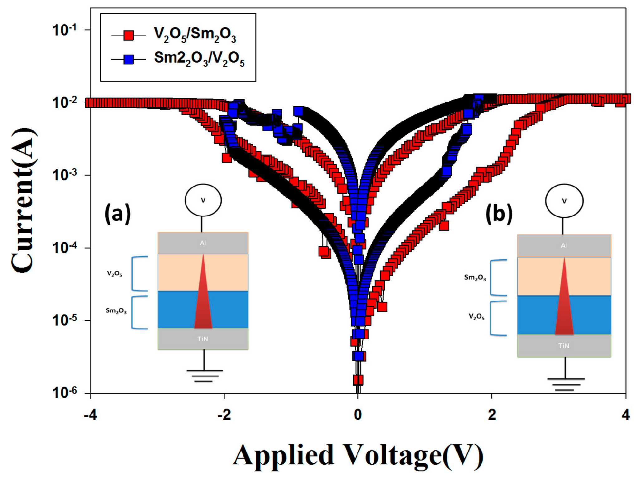
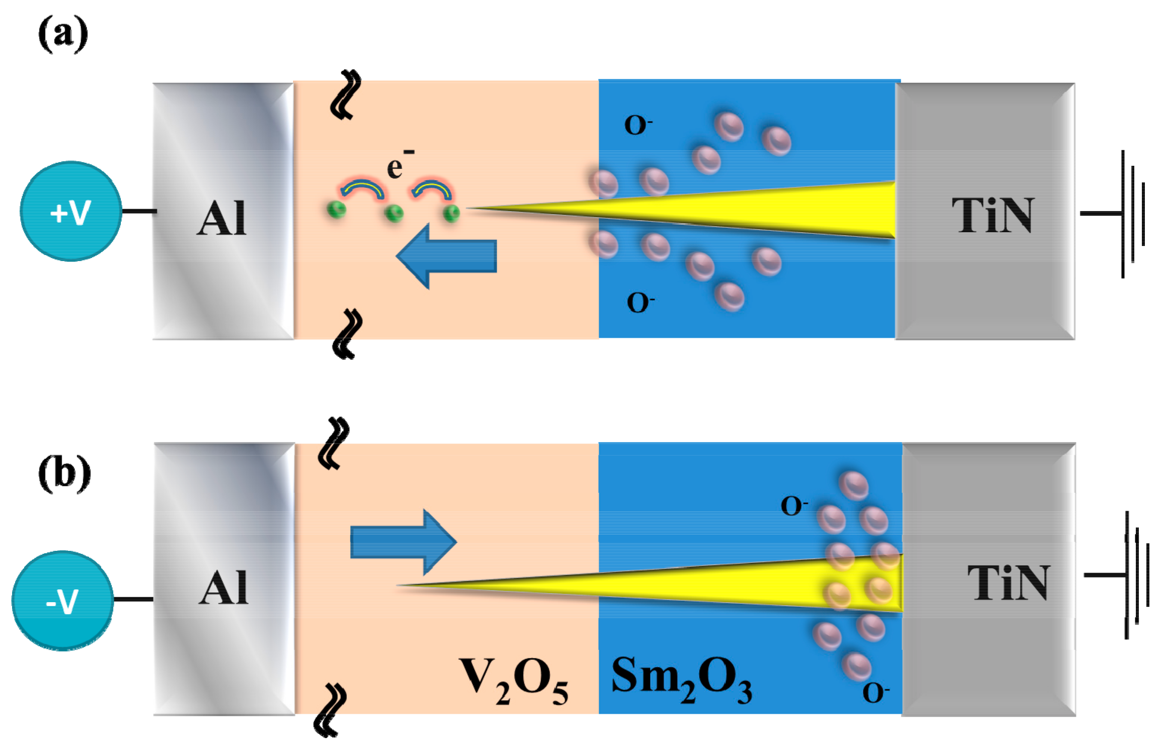
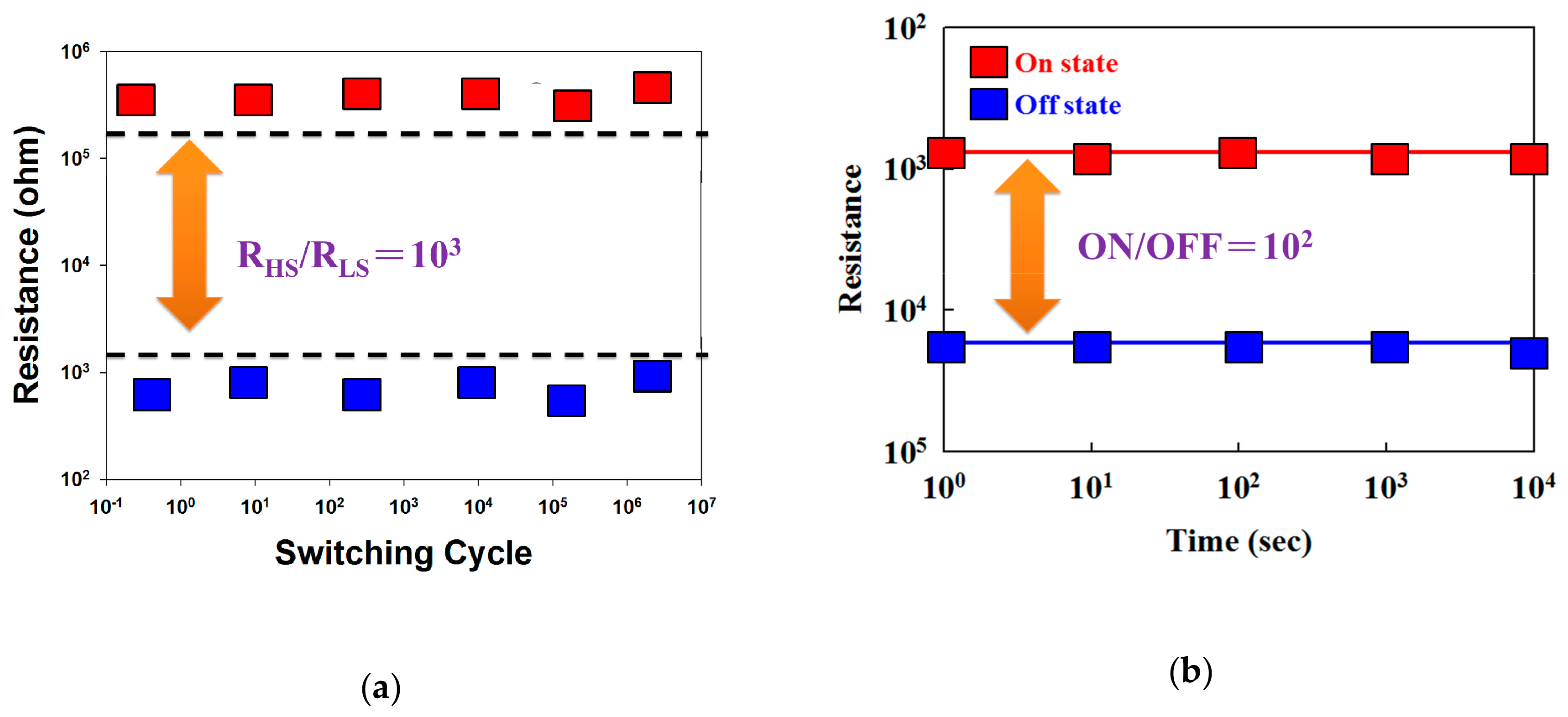
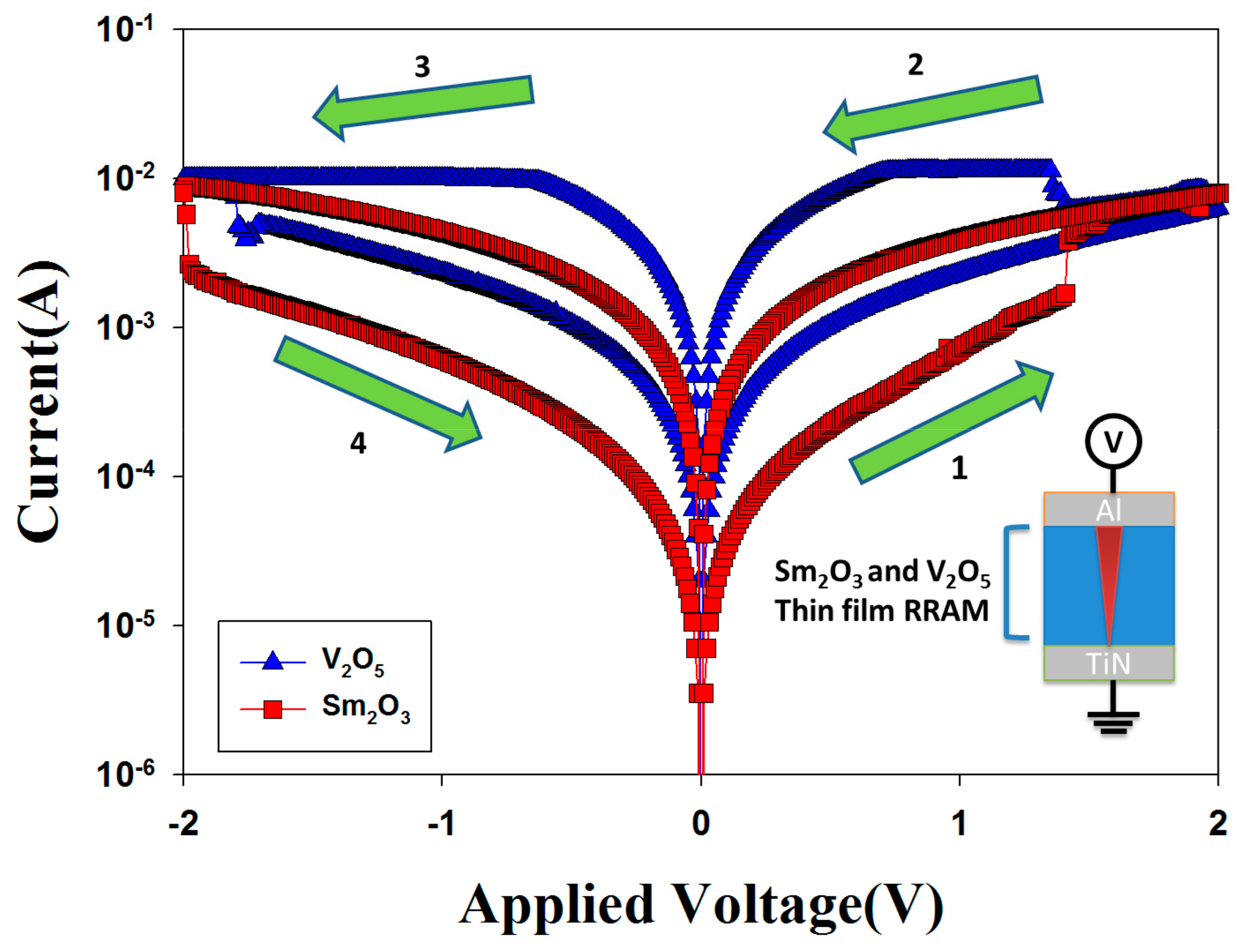
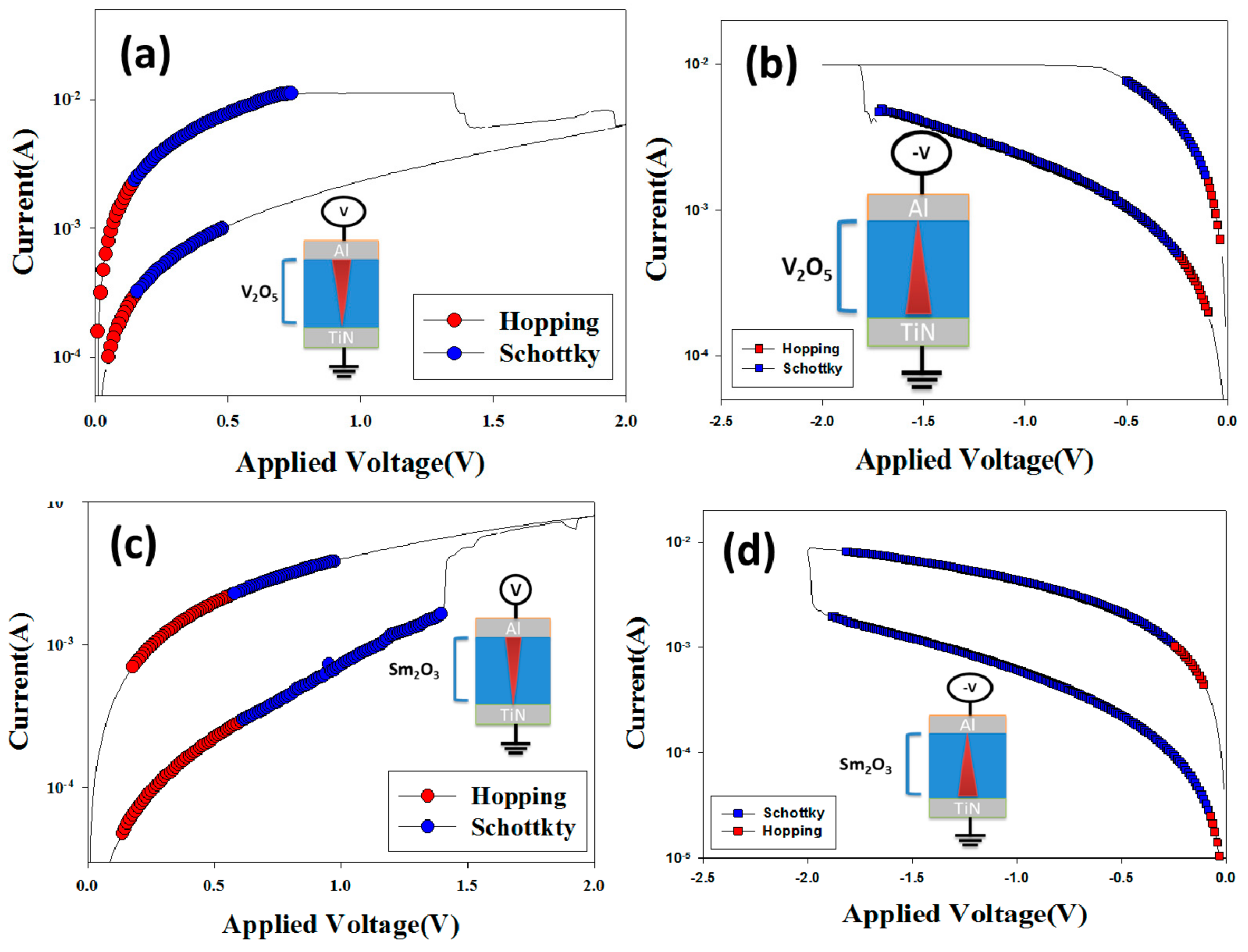
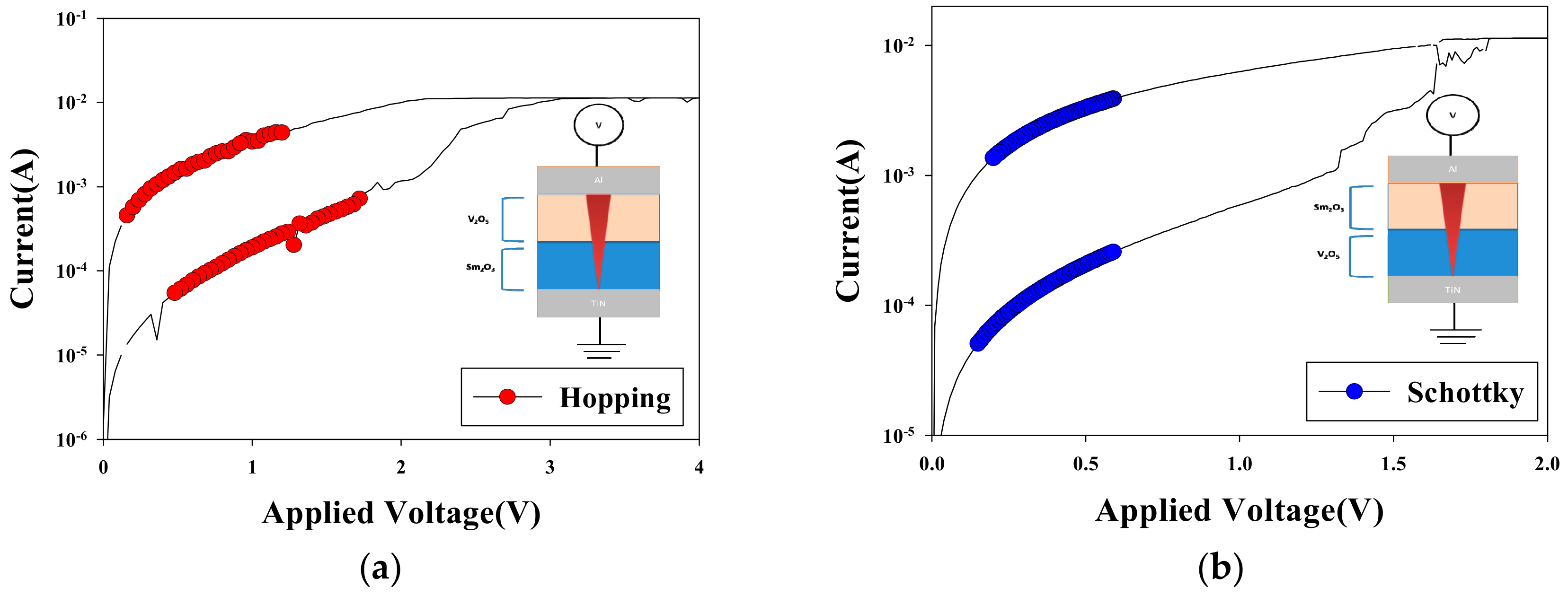
3. Results and Discussion
4. Conclusions
Author Contributions
Funding
Acknowledgments
Conflicts of Interest
References
- Murali, S.; Rajachidambaram, J.S.; Han, S.Y.; Chang, C.H.; Herman, G.S.; Conley, J.F., Jr. Resistive switching in zinc-tin-oxide. Solid State Electron. 2013, 79, 248–252. [Google Scholar] [CrossRef]
- Ismail, M.; Talib, I.; Rana, A.M.; Ahmad, E.; Nadeem, M.Y. Performance stability and functional reliability in bipolar resistive switching of bilayer ceria based resistive random access memory devices. J. Appl. Phys. 2015, 117, 084502. [Google Scholar] [CrossRef]
- Liang, D.; Li, X.; Wang, J.; Wu, L.; Chen, P. Light-controlled resistive switching characteristics in ZnO/BiFeO3/ZnO thin film. Solid State Electron. 2018, 145, 46–48. [Google Scholar] [CrossRef]
- Cheng, C.H.; Chou, K.I.; Zheng, Z.W.; Hsu, H.H. Low power resistive random access memory using interface engineered dielectric stack of SiOx/a-Si/TiOy with 1D1R-like structure. Curr. Appl. Phys. 2014, 14, 139–143. [Google Scholar] [CrossRef]
- Guo, J.; Ren, S.; Wu, L.; Kang, X.; Chena, W.; Zhao, X. Low power, high uniform, and forming-free resistive memory based on Mg-deficient amorphous MgO film with rough surface. Appl. Surf. Sci. 2018, 434, 1074–1078. [Google Scholar] [CrossRef]
- Pan, X.; Shuai, Y.; Wu, C.; Luo, W.; Sun, X.; Yuan, Y.; Zhou, S.; Ou, X.; Zhang, W. Resistive switching behavior in single crystal SrTiO3 annealed by laser. Appl. Surf. Sci. 2016, 389, 1104–1107. [Google Scholar] [CrossRef]
- Xu, D.; Xiong, Y.; Tang, M.; Zeng, B. Coexistence of the bipolar and unipolar resistive switching behaviors in vanadium doped ZnO films. J. Alloy. Compd. 2014, 584, 269–272. [Google Scholar] [CrossRef]
- Xiaoying, W.; Ming, H.; Kailiang, Z.; Fang, W.; Kai, L. Study on microstructure and resistance characteristic of vanadium oxide thin films. Acta Phys. Sin. 2013, 62, 47–201. [Google Scholar]
- Pan, T.M.; Lu, C.H. Switching behavior in rare-earth films fabricated in full room temperature. IEEE Trans. Electron Devices 2012, 59, 956–961. [Google Scholar] [CrossRef]
- Manjunath, V.; Reddy, V.R.; Reddy, P.R.S.; Janardhanam, V.; Choi, C.J. Electrical and frequency-dependent properties of Au/Sm2O3/n-GaN MIS junction with a high-k rare earth Sm2O3 as interlayer. Curr. Appl. Phys. 2017, 17, 980–988. [Google Scholar] [CrossRef]
- Karpov, V.G.; Niraula, D. OFF State Conduction in Filamentary RRAM. IEEE Trans. Electron Devices Lett. 2019, 40, 550–553. [Google Scholar] [CrossRef]
- Chin, W.C.; Cheong, K.Y.; Hassan, Z. Sm2O3 gate dielectric on Si substrate. Mater. Sci. Semicon. Process. 2010, 13, 303–314. [Google Scholar] [CrossRef]
- Sen, B.; Wong, H.; Molina, J.; Iwai, H.; Ng, J.A.; Kakushima, K.; Sarkar, C.K. Trapping characteristics of lanthanum oxide gate dielectric film explored from temperature dependent current-voltage and capacitance-voltage measurements. Solid State Electron. 2007, 51, 475–480. [Google Scholar] [CrossRef]
- Choi, J.S.; Kim, J.S.; Hwang, I.R.; Hong, S.H.; Jeon, S.H.; Kang, S.O.; Park, B.H.; Kim, D.C.; Lee, M.J.; Seo, S. Different resistance switching behaviors of NiO thin films deposited on Pt and SrRuO3 electrodes. Appl. Phys. Lett. 2009, 95, 022109. [Google Scholar] [CrossRef]
- Sun, X.; Li, G.; Zhang, X.; Ding, L.H.; Zhang, W.F. Coexistence of the bipolar and unipolar resistive switching behaviours in Au/SrTiO3/Pt cells. J. Phys. D Appl. Phys. 2011, 44, 125–404. [Google Scholar] [CrossRef]
- Chae, S.C.; Lee, J.S.; Kim, S.J.; Lee, S.B.; Chang, S.H.; Liu, C.; Kahng, B.; Shin, H.; Kim, D.W.; Shin, H.; et al. Random circuit breaker network model for unipolar resistance switching. Adv. Mater. [CrossRef]
- Lin, J.Y.; Wu, K.Y.; Chen, K.H.; Cheng, C.M.; Li, C.Y. Bipolar switching properties of bilayer V2O5/Sm2O3 thin-film resistive random access memory device prepared by sputtering technology. Sens. Mater. 2018, 30, 933–938. [Google Scholar]
- Tsai, T.M.; Chang, K.C.; Chang, T.C.; Syu, Y.E.; Chuang, S.L. Low temperature improvement method on Zn:SiOx, resistive random access memory devices. IEEE Electron Device Lett. 2013, 34, 511–513. [Google Scholar]
- Tsai, T.M.; Chang, K.C.; Chang, T.C.; Chang, G.W.; Syu, Y.E. Charge quantity influence on resistance switching characteristic during forming process. IEEE Electron Device Lett. 2013, 34, 502–504. [Google Scholar]
- Chen, K.H.; Tsai, T.M.; Cheng, C.M.; Huang, S.J.; Chang, K.C.; Liang, S.P.; Young, T.F. Schottky emission distance and barrier height properties of bipolar switching Gd:SiOx RRAM devices under different oxygen concentration environments. Materials 2018, 11, 43. [Google Scholar] [CrossRef]
- Chen, K.H.; Cheng, C.M.; Li, C.Y.; Huang, S.J. Hopping conduction distance of bipolar switching GdOx resistance random access memory thin films devices modified by different constant compliance current. Microelectron. Reliab. 2018, 91, 330–334. [Google Scholar] [CrossRef]


© 2019 by the authors. Licensee MDPI, Basel, Switzerland. This article is an open access article distributed under the terms and conditions of the Creative Commons Attribution (CC BY) license (http://creativecommons.org/licenses/by/4.0/).
Share and Cite
Lin, J.-Y.; Wu, K.-Y.; Chen, K.-H. Effects of Sm2O3 and V2O5 Film Stacking on Switching Behaviors of Resistive Random Access Memories. Crystals 2019, 9, 318. https://doi.org/10.3390/cryst9060318
Lin J-Y, Wu K-Y, Chen K-H. Effects of Sm2O3 and V2O5 Film Stacking on Switching Behaviors of Resistive Random Access Memories. Crystals. 2019; 9(6):318. https://doi.org/10.3390/cryst9060318
Chicago/Turabian StyleLin, Jian-Yang, Kuang-Yao Wu, and Kai-Huang Chen. 2019. "Effects of Sm2O3 and V2O5 Film Stacking on Switching Behaviors of Resistive Random Access Memories" Crystals 9, no. 6: 318. https://doi.org/10.3390/cryst9060318
APA StyleLin, J.-Y., Wu, K.-Y., & Chen, K.-H. (2019). Effects of Sm2O3 and V2O5 Film Stacking on Switching Behaviors of Resistive Random Access Memories. Crystals, 9(6), 318. https://doi.org/10.3390/cryst9060318