1. Introduction
III-nitride compounds have been extensively studied for applications in optoelectronics [
1,
2] and spintronics [
3,
4]. Recently, the GaN-based micro light-emitting diodes (LEDs) have attracted worldwide attention as energy-sustainable lighting sources and for use in full-color displays due to their compact size, high efficiency, and reliability. [
5,
6] However, micro-LEDs based on InGaN/GaN quantum wells (QWs) are limited by the poor quality of high-indium-content In
xGa
1-xN/GaN QWs (i.e., x > 0.33; so-called green gap) for use in red-green-blue (RGB) full-color displays [
7]. Alternatively, some researchers have combined UV InGaN/GaN LED arrays with CdSe/ZnS nanocrystal quantum dots (QDs) for color conversion [
8,
9] or specialized nano-ring light-emitting diodes (NRLEDs) produced using nano-sphere lithography technology. [
10,
11] These methods struggled with either introducing foreign CdSe/ZnS QDs or using a nano-lithography for manufacturing. The method of nano-lithography involved reducing the volume of LEDs by an etching process, which resulted in damage to the LED sidewall. Therefore, if one can fabricate micro-LEDs using a single material system, i.e., In
xGa
1-xN/GaN QWs on self-assembled micro-metered GaN disks, the manufacturing of RGB micro-LED display will become more efficient by a simple process without any complicated nano-lithography. The bandgap energy of ternary compound In
xGa
1-xN can be tuned according to the indium content (x) from 0.7 eV (i.e., InN for x = 1) to 3.4 eV (i.e., GaN for x = 0). In other words, full-color RGB micro-LED displays can be achieved by the single material system In
xGa
1-xN/GaN QW with various indium contents (e.g., x ~ 0.13 for blue, x ~ 0.28 for green, and x ~ 0.45 for red). [
12,
13,
14] However, as the indium volatilized temperature is about 650 °C, it is difficult to grow the In
xGa
1-xN layer with a high indium content by high-temperature growths like vapor phase epitaxy or metalorganic chemical vapor deposition. [
15] Currently, M. Azadmand et al. studied a droplet-controlled growth dynamics of InGaN/GaN on Si(111) substrate by plasma-assisted molecular beam epitaxy (PAMBE) at low temperatures (e.g., 450 °C), in which the Si(111) substrate provided a hexagonal basis for the growth of
c-plane (0001) wurtzite GaN film. [
16] In contrast, Lo et al. developed a low-temperature growth of hexagonal
c-plane wurtzite GaN microdisks on LiAlO
2 (LAO) substrates by PAMBE, where the LAO substrate provided a hexagonal basis for the growth of
c-plane (000
) GaN and meanwhile offered a rectangular basis for
M-plane (1
00) GaN growth. [
17] It was shown that 3-dimensional (3D) hexagonal
c-plane GaN (000
) microdisk was grown atop the hexagonal oxygen sites of LAO substrate as a finite GaN microdisk was formed. [
18] The 3D GaN microdisk can be used as a “nearly” free-standing GaN substrate for the further growth of In
xGa
1-xN/GaN, as shown in
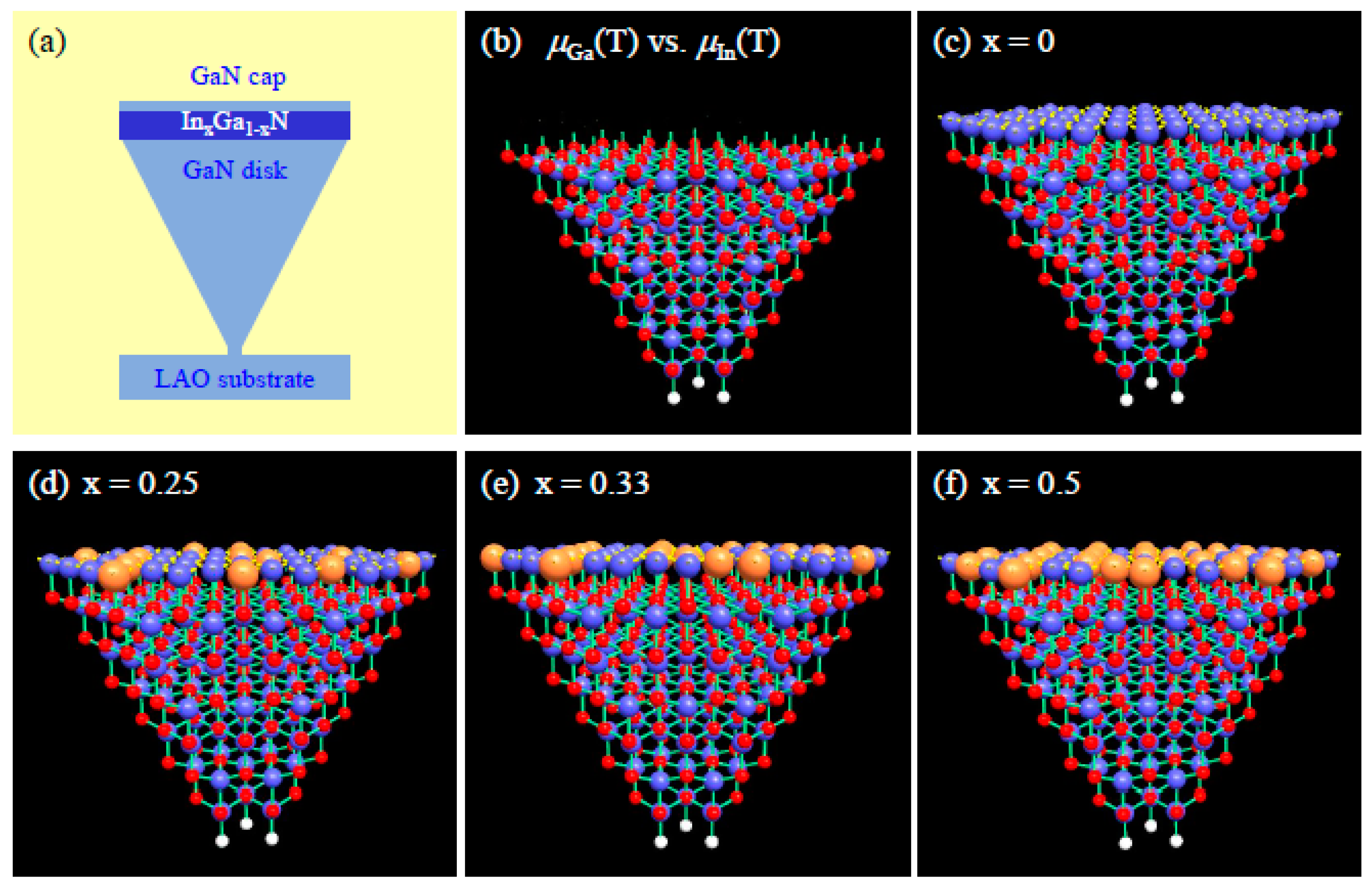
Figure 1a. However, the lattice constant between GaN (
a = 0.3160 nm,
c = 0.5125 nm) and InN (
a = 0.3545 nm,
c = 0.5703 nm) is quite different, the fabrication of ternary In
xGa
1-xN alloy on the 3D GaN microdisk is crucial for the In
xGa
1-xN/GaN micro-LED manufacturing. The nucleation of Ga or In atoms is the first step in the formation of In
xGa
1-xN layers for self-assembling on N-face, which depends on the thermodynamic chemical potentials of Ga and In ions at equilibrium,
μGa(T) and
μIn(T), as shown in
Figure 1b. After the nucleation, the In-content (x) of ternary In
xGa
1-xN alloy will be affected by the flux ratios between Ga and In molecular beams. The ball-stick model of the ternary In
xGa
1-xN alloy starting to grow onto N-face layer of GaN microdisk is simulated with different indium contents, as shown in
Figure 1c–f; here, we do not include the lattice deformation due to strain. Therefore, the self-assembling mechanism for different indium contents can be controlled by growth parameters (e.g., substrate temperature and element flux ratio). In this paper, we will systematically study the growth mechanism for the alloy composition of In
xGa
1-xN layer on GaN microdisk as functions of growth temperature and flux ratio using low-temperature PAMBE. Based on the results, we demonstrate the growth of high-indium-content In
xGa
1-xN/GaN quantum well on GaN microdisk for RGB micro-LED applications.
2. Materials and Methods
The ternary In
xGa
1-xN epi-layers were grown on GaN microdisks on 1 x 1 cm
2 LAO substrates by PAMBE (Veeco Applied-GEN 930 (Hsinchu, Taiwan)) with standard effusion cells for Ga- and In-evaporation and an rf-plasma cell with 450 W for N
2-plasma source. The detailed procedure can be found in our previous papers [
17,
18]. Before mounting on a holder, the LAO substrates were cleaned with acetone (5 min), isopropanol (5 min), de-ionized water (5 sec), phosphoric acid (1:30) (5 min), de-ionized water (5 sec), and then dried by nitrogen gas, sequentially. After the cleaning, the LAO substrates were out-gassed in MBE chamber at 680 °C for 10 min. Thereafter, the substrate temperature was decreased to the growth temperatures (T
S) specified for the study. The Ga wetting layer was first deposited on the LAO substrate for 5 min at 630 °C, and then a two-step method (i.e., two different N/Ga flux ratios, 29.0 and 138.8, performed for 35 min and 70 min, respectively) was used to grow 3D GaN microdisks at 630 °C. After the GaN epi-layer, we grew In
xGa
1-xN epi-layers on the 3D GaN microdisks for different growth parameters designed in
Table 1 and
Table 2. In sample series I, the In
xGa
1-xN epi-layers of five samples (samples A–E) were grown at a fixed N flux ratio (BEP = 9.0 x 10
−6 torr) but the different In/(In + Ga) flux ratios for 90 min at 620 °C, as shown in
Table 1. The flux ratio was measured by beam equivalent pressure (BEP) reading from Veeco Applied-GEN 930 system. In sample series II, another four samples with different In
xGa
1-xN epilayers were grown at different temperatures but using the same flux ratio as sample D for 90 min for comparison, labelled as samples F, G. H. and I. The detail growth parameters for sample series II are shown in
Table 2.
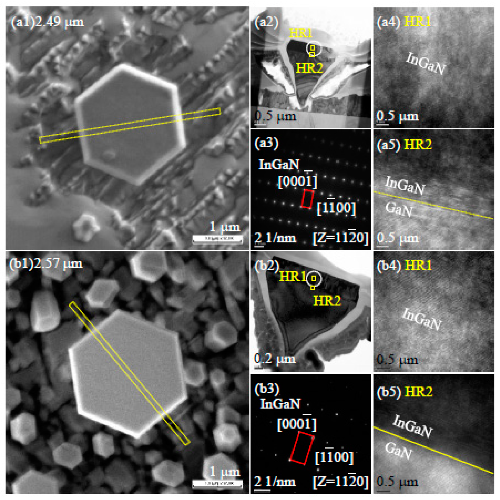
In order to examine the microstructure of the samples, two typical InGaN/GaN microdisk specimens were selected from samples D and H for scanning electron microscope (SEM), transmission electron microscope (TEM) and selective area electron diffraction (SAD) measurements. The TEM specimen was prepared by a dual-beam focus ion beam (FIB) along [1
00] direction, as shown in the
Figure 2(a1). The cross-sectional TEM image of 2.49 μm microdisk for sample D is shown in
Figure 2(a2). We performed the selection area diffraction (SAD) measurements on the In
xGa
1-xN layers at the spot circled in
Figure 2(a2). The SAD pattern exhibited a clear wurtzite single crystal as shown in
Figure 2(a3). The In
xGa
1-xN epi-layers were precisely evaluated by high-resolution TEM images focused on the spots HR1 and HR2, shown in
Figure 2(a4,a5).
Figure 2(a4) shows the
c-plane wurtzite InGaN and
Figure 2(a5) shows the interface between GaN and In
xGa
1-xN in sample D. The lattice deformation due to the different atomic size can be clearly observed from the In
xGa
1-xN epi-layers in
Figure 2(a5). Similarly, the TEM specimen of sample H was prepared,
Figure 2(b1). The cross-sectional TEM image of the 2.57 μm microdisk is shown in
Figure 2(b2). We performed the SAD measurements on the In
xGa
1-xN layer at the spot circled in
Figure 2(b2). The SAD pattern exhibited a clear wurtzite crystal as shown in
Figure 2(b3). The In
xGa
1-xN epi-layers were evaluated by high-resolution TEM images on the spots HR1 and HR2, shown in
Figure 2(b4,b5).
Figure 2(b4) shows the well-established
c-plane wurtzite InGaN and
Figure 2(b5) shows the interfaces between GaN and InGaN layers in sample H. Again, the slight lattice deformation of In
xGa
1-xN epi-layers can be observed in
Figure 2(b5), due to the different sizes between Ga and In atoms.
3. Results and Analyses
In
xGa
1-xN/GaN microdisks of the two series samples were systematically used to evaluate optical properties by cathodoluminescence (CL) and secondary electron images (SEI) measurements (JEOL JSM-6330).
Figure 3 shows the results of CL measurement for series I samples. We obtained the CL spectra by detecting the photon energy from 1.8 eV to 3.7 eV at accelerative voltage of 10 kV and extraction voltage of photonelectric magnitude tube of 1.1 kV. In sample A, we observed the highest peak at (2.56 ± 0.003) eV with FWHM equal to (0.088 ± 0.003) eV, the secondary peak at (3.35 ± 0.003) eV with FWHM equal to (0.091 ± 0.007) eV, and the smallest peak at (3.57 ± 0.005) eV with FWHM equal to (0.082 ± 0.003) eV. The SEI and the CL image at the highest peak are shown in
Figure 3(a1,a2). The CL image shows that the highest peak for the wavelength of 480 nm (e.g., 2.58 eV) was majorly emitted from the In
xGa
1-xN layer itself. The secondary peak (i.e., 3.35 eV) was normally contributed from the GaN layer and the third peak (i.e., 3.57 eV) might be attributed to the microstructures around the InGaN/GaN microdisk. In sample B, we observed the first peak at (2.13 ± 0.005) eV with FWHM equal to (0.137 ± 0.005) eV, the secondary peak at (3.33 ± 0.003) eV with FWHM equal to (0.059 ± 0.004) eV. The SEI and CL images are shown in
Figure 3(b1,b2), with the CL image shown at the peak of wavelength 580 nm (e.g., 2.14 eV). In sample C, we observed the first peak at (2.11 ± 0.005) eV with FWHM equal to (0.195 ± 0.008) eV, the secondary peak at (3.38 ± 0.003) eV with FWHM equal to (0.044 ± 0.004) eV. The SEI and CL images are shown in
Figure 3(c1,c2). The CL image shows the peak for wavelength of 587 nm (e.g., 2.11 eV). In sample D, we observed the first peak at (2.10 ± 0.009) eV with FWHM equal to (0.258 ± 0.009) eV, the secondary peak at (3.39 ± 0.005) eV with FWHM equal to (0.045 ± 0.006) eV. The SEI and CL images are shown in
Figure 3(d1,d2). The CL image shows the peak for wavelength of 570 nm (e.g., 2.11 eV). In sample E, we observed the first peak at (2.21 ± 0.009) eV with FWHM equal to (0.153 ± 0.003) eV, the secondary peak at (3.37 ± 0.003) eV with FWHM equal to (0.061 ± 0.002) eV. The SEI and CL images are shown in
Figure 3(e1,e2). The CL image shows the peak for wavelength of 560 nm (e.g., 2.21 eV). From the spectra in
Figure 3, we found that the CL intensity from In
xGa
1-xN of sample A was about 52 times that from GaN intensity. The CL intensity of In
xGa
1-xN for sample B, sample D, and sample E were about 0.73, 0.32, and 0.32 times those from GaN intensity, respectively, and the CL images of In
xGa
1-xN of microdisks had no detectable luminescence, as shown in
Figure 3(b2,d2,e2). Because we did not introduce any extrinsic impurity during the epitaxy, the broad CL peak with large FWHM was mostly contributed from the structural defects including dislocations, stacked faults and lattice deformations. The broad secondary peak with large FWHM spectra indicated that the lattice deformation occurred after introducing the indium atoms into In
xGa
1-xN layers due to the greater atomic size of indium; e.g., x = 0.33 as shown in
Figure 1(d). The CL intensity from In
xGa
1-xN in sample C was about 0.72 times that from GaN intensity.
Figure 3(c1,c2) show that the position of the illuminating was around the microdisk. The CL peaks, FWHMs, and In contents for the samples of series I are summarized in
Table 3.
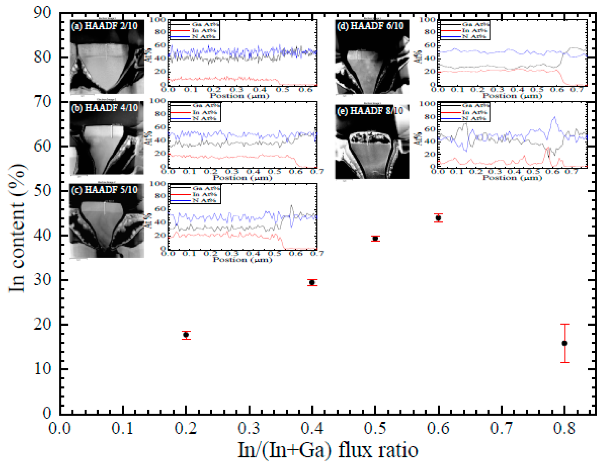
In order to evaluate the constituents of In
xGa
1-xN epi-layers, the energy dispersive x-ray spectroscopy (EDS) measurement was performed on the TEM specimens cut from the five series I samples. We prepared the TEM specimens along the (11
0) direction and scanning EDS with s zone axis (10
0). The result of indium content (x) as a function of In/(In + Ga) flux ratio is shown in
Figure 4. In the insets,
Figure 4a–e show the high angle annular dark field (HAADF) TEM images performed in the line EDS scanning mode with the constituent spectra for samples A–E, where the scanning lines were marked on the TEM images. We obtained the EDS constituent spectra (at %) from top surface crossing the In
xGa
1-xN layers to the GaN microdisk; Ga content (at %) indicated by black EDS spectrum, In content (at %) by red EDS spectrum and N content (at %) by blue EDS spectrum in the insets. We take an average from the EDS spectra of In
xGa
1-xN layers and obtain the indium content of sample A to be (17.8 ± 0.92 %), sample B to be (29.5 ± 0.73 %), sample C to be (39.3 ± 0.67 %), sample D to be (44.2 ± 0.83 %), and sample E to be (15.9 ± 4.3 %). It was found that the content of indium increased when we grew the In
xGa
1-xN layer with the In/(In + Ga) flux ratio from 0.2 to 0.6 at the temperature of 620 °C, and dropped quickly when the ratio In/(In + Ga) is up to 0.8. It is shown in the dark field TEM image
Figure 4e that the compressive lattice deformation destroyed the shape of wurtzite lattice structure after the incorporation of indium. This is consistent with the worst CL spectrum of sample E shown in
Figure 3.
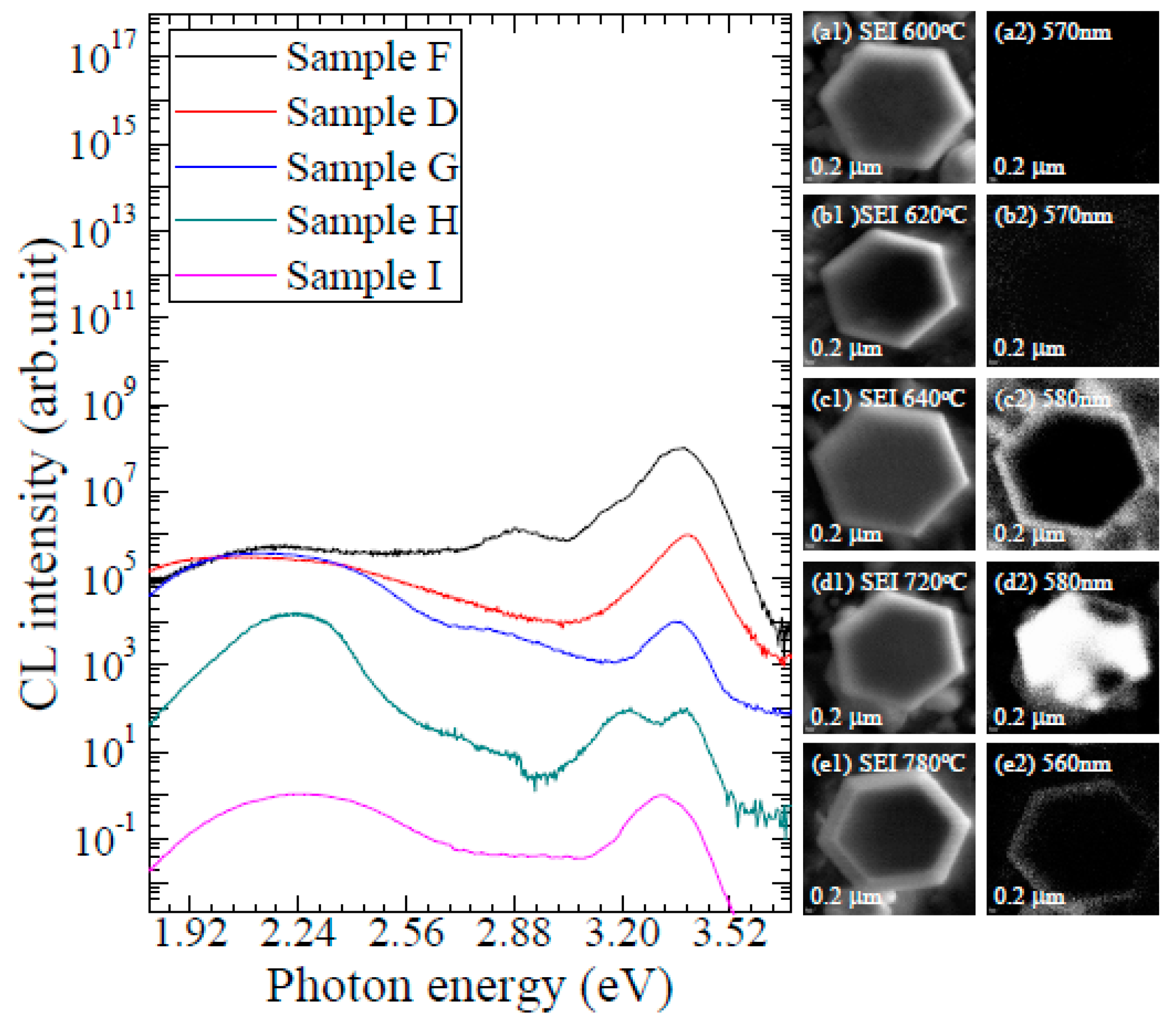
Similar analyses were performed on the series II samples against the growth temperature, where sample D was the same sample as series I for comparison. The results of CL measurements of the series II samples are shown in
Figure 5. In sample F, we observed the first peak at (2.21 ± 0.008) eV with FWHM equal to (0.204 ± 0.005) eV, the secondary peak at (2.90 ± 0.005) eV with FWHM equal to (0.083 ± 0.003) eV, and the third peak at (3.37 ± 0.002) eV with FWHM equal to (0.054 ± 0.002) eV. The SEI and CL images are shown in
Figure 5(a1,a2), where the CL image shows that the peak for wavelength of 570 nm (e.g., 2.18 eV). For sample D, the CL spectrum is the same as that in
Figure 3 for comparison, and the SEI and CL images are shown in
Figure 5(b1,b2). In sample G, we observed the first peak at (2.15 ± 0.004) eV with FWHM equal to (0.184 ± 0.004) eV and the secondary peak at (3.36 ± 0.003) eV with FWHM equal to (0.046 ± 0.002) eV. The SEI and CL images are shown in
Figure 5(c1,c2). The CL image shows the peak for wavelength of 580 nm (e.g., 2.14 eV). In sample H, we observed the first peak at (2.22 ± 0.004) eV with FWHM equal to (0.098 ± 0.005) eV, the secondary peak at (3.22 ± 0.004) eV with FWHM equal to (0.120 ± 0.006) eV and the third peak at (3.38 ± 0.002) eV with FWHM equal to (0.075 ± 0.003) eV. The SEI and CL images are shown in
Figure 5(d1,d2). The CL image shows the peak for wavelength of 580 nm (e.g., 2.14 eV). In sample I, we observed the first peak at (2.25 ± 0.006) eV with FWHM equal to (0.165 ± 0.007) eV and the secondary peak at (3.32 ± 0.002) eV with FWHM equal to (0.057 ± 0.003) eV. The SEI and CL images are shown in the
Figure 5(e1,e2). The CL image shows the peak for wavelength of 560 nm (e.g., 2.21 eV). From the CL spectra in
Figure 5, we found that the In
xGa
1-xN intensity of sample H was about 170 times that of the GaN intensity.
Figure 5(d1,d2) show that the position of the illuminating was from the microdisk. The In
xGa
1-xN intensity of sample G was about 40 times that of the GaN intensity.
Figure 5(c1,c2) show that the position of the illuminating was around the microdisk. The In
xGa
1-xN intensity of sample F was about 0.006 times that of GaN intensity, and the CL image of In
xGa
1-xN in microdisk had no detectable luminescence, as shown in
Figure 5(a1,a2). The In
xGa
1-xN intensity of sample I was about 1.13 times that of GaN intensity.
Figure 5(e1,e2) show that the position of the illuminating was around the microdisk edge. The CL peaks, FWHMs, and In contents for the samples of series II are summarized in
Table 4.
Again, we evaluate the constituents of In
xGa
1-xN layers in series II samples by energy dispersive x-ray spectroscopy (EDS) measurements. The TEM specimens were prepared along the (11
0) direction and scanning EDS line mode with the zone axis (10
0). The results are shown in
Figure 6. The high angle annular dark field (HAADF) TEM images and detailed EDS constituent spectra for series II samples are shown in the insets,
Figure 6a–e. The EDS spectra were covered from the top of In
xGa
1-xN layer and down to GaN miscrodisk. The indium content of sample F was (53.4 ± 0.75 %), sample D was (44.2 ± 0.83 %), sample G was (39.8 ± 0.62 %), sample H was (34.9 ± 0.72 %), and sample I was (0%).
Figure 6 shows that the content of indium decreased with the growth temperature from 600 °C to 720 °C for the epitaxy of In
xGa
1-xN layers. When the growth temperature was up to 780 °C, the indium content of In
xGa
1-xN layer dropped to zero. This reveals that the high temperature is not favorable for the high-indium-content epitaxy in ternary In
xGa
1-xN epi-layers due to the low indium volatilized temperature. Based on the results, we designed an appropriate In
xGa
1-xN layer as a buffer to grow high-indium-content In
xGa
1-xN/GaN microdisk double quantum wells. For instance, after GaN microdisk, we grew the In
xGa
1-xN layers as a buffer with flux ratio of (In:Ga:N) to be (9.01 x 10
−8 torr: 6.02 × 10
−8 torr: 8.96 × 10
−6 torr) at temperature of 720 °C for 50 minutes, and capped with a GaN layer for the further growth of In
xGa
1-xN/GaN double QWs. The double QWs were grown after the buffer layer with the flux ratio of (In:Ga:N) to be (9.01 × 10
−8 torr: 6.02 × 10
−8 torr: 8.96 × 10
−6 torr) for 1.5 minutes and the flux ratio of (Ga:N) to be (6.02 × 10
−8 torr: 9.08 × 10
−6 torr) for 30 seconds, and finally the GaN barrier was grown on the GaN cap layer for 5 min with the flux ratio of (Ga:N) to be (1.28 × 10
−7 torr: 8.96 × 10
−6 torr). This sequence of In
xGa
1-xN/GaN epi-layers was repeated twice to form In
xGa
1-xN/GaN double QWs.
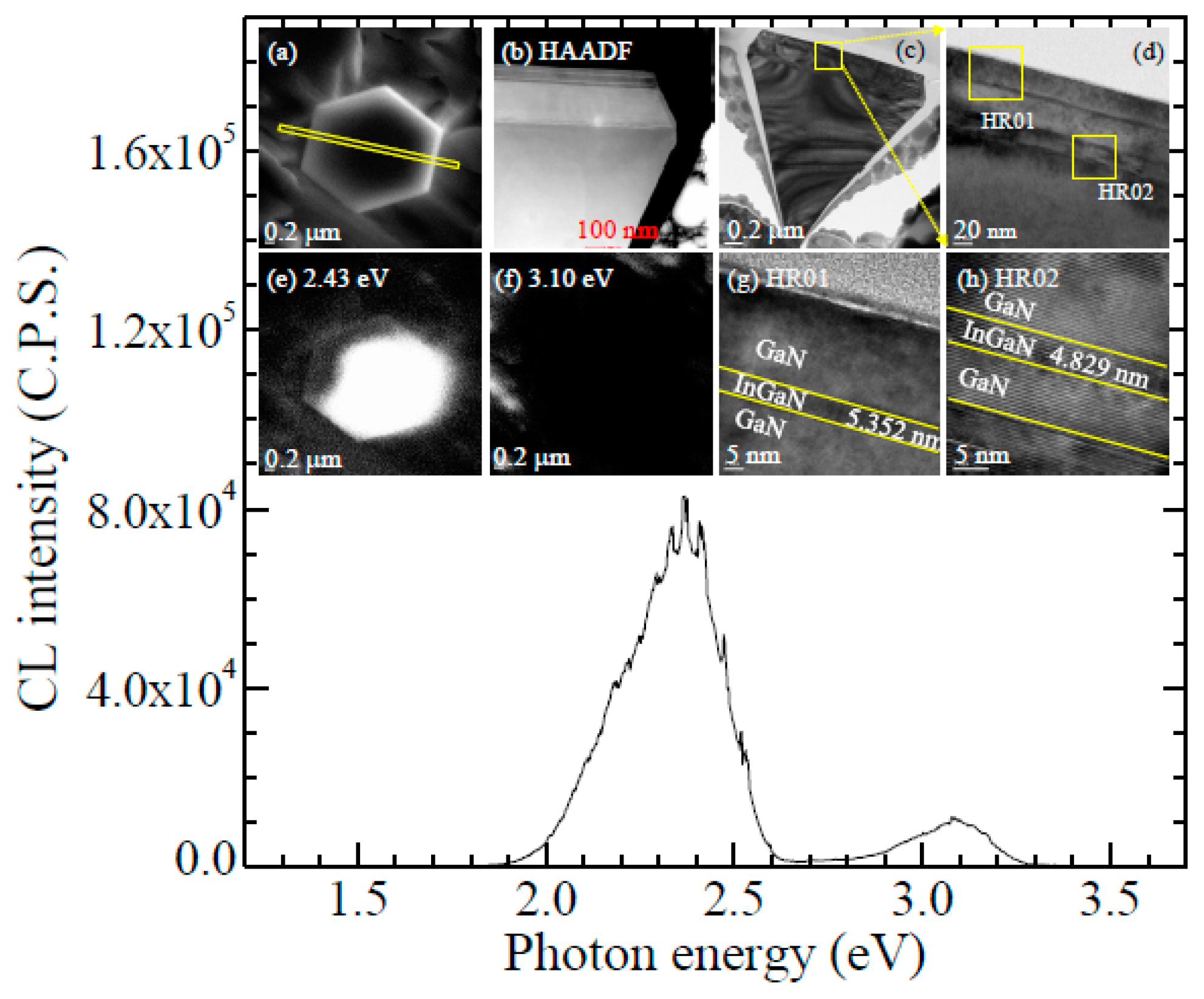
Figure 7 shows the CL spectrum of the In
xGa
1-xN/GaN microdisk double QWs, in which the intensity of CL peak at 2.43 eV is about one order of amplitude higher than that at 3.1 eV. The SEM image of the microdisk double QWs is shown in the inset,
Figure 7a. The In
xGa
1-xN buffer and double-QW structure can be observed from the TEM images,
Figure 7b–d.
Figure 7e,f show that the CL images of the peak at 2.43 eV, which is mostly emitted from the In
xGa
1-xN layers with the In content of x = 0.27 and the CL peak at 3.1 eV which is from microstructures around the microdisk. To confirm the quality of the double QWs, high resolution TEM images were taken at the spots HR01 and HR02, as shown in
Figure 7d. The well-assembled GaN lattice and In
xGa
1-xN lattice are shown in
Figure 7g,h. The slight lattice deformation can only be observed in the In
xGa
1-xN layers from high resolution TEM images.


