Article

Optimal Sr-Doped Free TiO2@SrTiO3 Heterostructured Nanowire Arrays for High-Efficiency Self-Powered Photoelectrochemical UV Photodetector Applications

Department of Optoelectronic Information Science, School of Materials Science and Engineering, Harbin Institute of Technology, Harbin 150001, China
*
Authors to whom correspondence should be addressed.
Crystals 2019, 9(3), 134; https://doi.org/10.3390/cryst9030134
Submission received: 31 January 2019 / Revised: 27 February 2019 / Accepted: 28 February 2019 / Published: 6 March 2019

Abstract

:
Due to their high performance, photoelectrochemical ultraviolet (UV) photodetectors have attracted much attention, but the recombination of photogenerated electrons at the interface of photoanode/electrolyte limited further improvement of photoelectrochemical UV photodetectors (PEC UVPDs). Modification of TiO2 photoanode by SrTiO3 could improve the performance of UVPD, because the energy barrier that is established at the TiO2–SrTiO3 interface could accelerate the separation of the photogenerated electrons-holes pair. However, the recombination center that is caused by the preparation of TiO2@SrTiO3 core-shell heterostructured nanostructure decreases the performance of PEC UVPDs, which is still an important problem that hindered its application in PEC UVPDs. In this paper, we presented a Sr-doped free TiO2@SrTiO3 core-shell heterostructured nanowire arrays as a photoanode for the self-powered PEC UVPD. This will not only accelerate the separation of the photogenerated electrons-holes pair, but it will also reduce the recombination of photogenerated electron-hole pairs in the photoanode. The intrinsic effect of SrTiO3 reaction time on the J variations of UVPDs is investigated in detail. An impressive responsivity of 0.358 A·W−1 was achieved at 360 nm for the UVPD based on TiO2@SrTiO3 core-shell heterostructured nanowire arrays, which heretofore is a considerably high photoresponsivity for self-powered photoelectrochemical UVPDs. Additionally, this UVPD also exhibits a high on/off ratio, fast response time, excellent visible-blind characteristic, and linear optical signal response.

Graphical Abstract

1. Introduction

Due to important application in environmental monitoring and surveillance, missile warning, chemical and physiology analyses, fire detection, and secure communication, the precise detection of ultraviolet (UV) radiation is desperately in demand [1]. Semiconductor UV photodetectors (UVPDs) can be categorized into two types: photoconductive and photovoltaic. The photoconductive UVPDs cannot operate without extra power sources, which is applied to urge the photogenerated carriers to generate a photocurrent [2,3,4,5,6]. This largely enlarges the device size and weight, which leads to the disadvantages of miniaturization, wireless applications, and intellectualization.
Recently, the demand for UV photodetectors that could work without additional power sources has become more and more urgent [7,8,9,10,11]. A series of self-powered UVPDs have been reported and they draw a great deal of attention on account of their numerous merits [12,13,14,15,16,17]. This type of UVPD has been designed by utilizing the photovoltaic effect. According to the charge separation features of the interface, the UVPDs that are based on the photovoltaic effect can be divided into three main types: p–n junction, Schottky junction, and photoelectrochemical (PEC) cell. For the PEC-type UVPDs, a simple physicochemical process, which could reduce the preparation process complexity when compared with p-prepares n junction and Schottky junction UVPDs, prepare photoanodes and counter electrodes. Furthermore, PEC UVPDs could generate a larger current, up to mA, which could be easily detected [18,19,20,21,22]. Based on the preparation of photoanode on flexible substrates [23], the PEC UVPDs could have a wider application range due to their weight reduction and better mechanical flexibility [24]. In summary, research on PEC UVPDs has great significance.
Researchers have used different materials, micro-/nano-structures, electrolytes, counter electrodes, and even varied device structures to assemble PEC UVPDs to enhance the performance of UV detecting. To date, most efforts to improve the performances of PEC UVPDs has concentrated on developing photoanodes. Diverse nanostructures were employed for fabricating photoanode in PEC UVPDs, including nanoparticle (NP), nanosheet (NS), nanorod (NR), nanotube (NT), nanowire (NW), and nano forest (NF) [25]. The electron transport rates and the specific surface area (SSA) of these nanostructures mentioned above cannot be gotten simultaneously. Conventional nanocrystals photoanode require thermal sintering to strengthen the electronic contact between each particle, thus leading to added processing overhead, hindering the application of flexible substrates [26]. By contrast, one-dimensional (1D) nanostructure semiconductors, such as NWs, are candidates with great promise for high performance PEC UVPDs, because a 1D nanostructure could provide direct an electron transport tunnel to accelerate the separation of carriers to reduce the possibility of the recombination of photogenerated electrons [27,28,29,30]. Xie and coworkers reported the self-powered UVPDs based on 1D TiO2 nanorod arrays. The photosensitivity of UVPDs are 0.22 A·W−1, which are greatly enhanced when compared with the nanocrystalline TiO2 film based UVPD [17]. Thanks to the great developments in fabrication techniques, most semiconductor NWs could have been successfully synthesized [31,32].
Meantime, the energy gap of the photoanode materials for PEC UVPDs should be larger than 3.1 eV, relating to the wavelength of ultraviolet radiation. In the past several decades, the investigated wide bandgap oxide and sulfide nanomaterials, including ZnO [20], ZnS [33], TiO2 [34], SnO2 [35], and perovskite structure oxides, like SrTiO3 [36], can be possibly employed as photoanode materials for PEC UVPDs. Among the various wide bandgap semiconductors, TiO2 is an n-type direct bandgap semiconductor with a proper bandgap and it has been widely investigated, owing to its UV absorption features [2,37].
A good deal of 1D TiO2 nanostructures have been applied as the photoanodes for PEC UVPDs [38,39,40,41,42]. The research of Cao et al. [40] suggests that a proper size of NRAs is essential for a higher photocurrent. Chen’s group employed vertical rutile TiO2 NRAs on PEC UVPDs, showing the responsivity of 25 mA·W−1 at 350 nm with a fast photoresponse [38]. Subsequently, they prepared branched TiO2 nanostructures that were based on TiO2 NRAs by a facile two-step chemical synthesis process. The PEC UVPDs based on branched TiO2 nanostructures showed the Rλ of 186.5 mA·W−1 at 365 nm with a low response time (the rise time of 0.15 s and the delay time of 0.05 s) Though, the superior light scattering characteristics of the branched TiO2 NRAs issue in higher harvesting of the optical light region is detrimental to the spectral selectivity of UVPD.
Commonly, the approaches for improving the performance of PEC UVPDs comprise three aspects: augmenting light capturing in UV region in photoanodes, raising charge separation or suppressing charge recombination at the interface of photoanode-electrolyte, and enhancing carrier transport [43]. Charge recombination at the interface of photoanode-electrolyte is a critical problem that exists in PEC UVPD, and the loss of photogenerated electrons leads to low responsivity [44]. Building semiconductor core–shell structures with type-II band alignment is a good way to suppress charge recombination at the interface of the photoanode-electrolyte, which has attracted plenty of interest for application as the photoanode of next generation photoelectrochemical cells. Semiconductor core–shell structures with type-II band alignment could establish a potential barrier at the interface of core–shell structures to suppress the recombination of the photogenerated electrons and the oxide of electrolyte and accelerate the separation of carriers. [45,46]. According to the energy levels that could form an energy potential barrier at the interface of photoanode-electrolyte, for TiO2 nanomaterials, the core–shell structures of TiO2@MgO [47], TiO2@InO [48], TiO2@WO3 [49], and TiO2@SrTiO3 show prodigious probability in high-efficiency PEC cells.
The performance of TiO2@SrTiO3 core-shell heterostructured nanostructures could be ulteriorly improved by employing the piezo-phototronic effect. As a general matter, elastic strain was introduced during the growth of epitaxial dissimilar materials core–shell nanostructures, such as nanowire arrays (NWAs) [50,51]. As a result, a static and internally built strain that is introduced by the lattice-mismatch can create piezoelectric polarization in the nanostructure [52,53]. The piezoelectric polarization in the core–shell NWAs is beneficial to the separation of the photogenerated electron-hole pairs.
The hydrothermal method is the most economical and practical for large size devices among the various effective methods for preparing TiO2@SrTiO3 core-shell heterostructured NWAs. In general, TiO2 NWAs and Sr2+ source was used to prepare the TiO2@SrTiO3 core-shell heterostructured NWAs. The reaction from TiO2 to SrTiO3 could be regarded as a simultaneous decomposition–deposition procedure that includes the decomposition of TiO2 followed by the deposition of the SrTiO3. When the break of TiO2 lattice occurred at the surface of TiO2 NWAs, the Sr2+ could diffuse into the lattice of TiO2 to form the Sr-doped TiO2@SrTiO3 heterostructures arrays. The doped Sr2+ may bring more recombination centers and oxygen vacancies in the TiO2@SrTiO3 heterostructure and damage the carrier transport pathway that is provided by the TiO2 nanowires. These lead to more recombination of photogenerated electron and the degradation of the of the PEC UVPD performance [54].
To solve the doped Sr2+ in TiO2@SrTiO3 heterostructures, in this paper, we present the Sr2+-doped free TiO2@SrTiO3 core-shell heterostructured NWAs as a photoanode for the self-powered PEC UVPD. When compared with the UVPD that is based on the bare TiO2 NWAs, the UVPD based on Sr2+-doped free TiO2@SrTiO3 core-shell heterostructured NWAs exhibits a higher responsivity and sensitivity (on/off ratio) under UV light irradiance. The effect of various preparation conditions of TiO2@SrTiO3 core-shell heterostructured NWAs is discussed in detail. Subsequently, the spectral-response characteristics, photo-sensitivity, response speed, and light intensity dependence of the J signal are also tested to estimate the performance of UVPD based on Sr2+–doped free TiO2@SrTiO3 core-shell heterostructured NWAs.

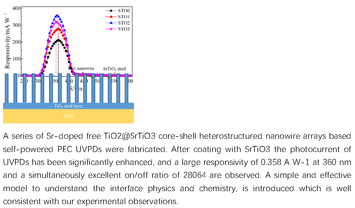
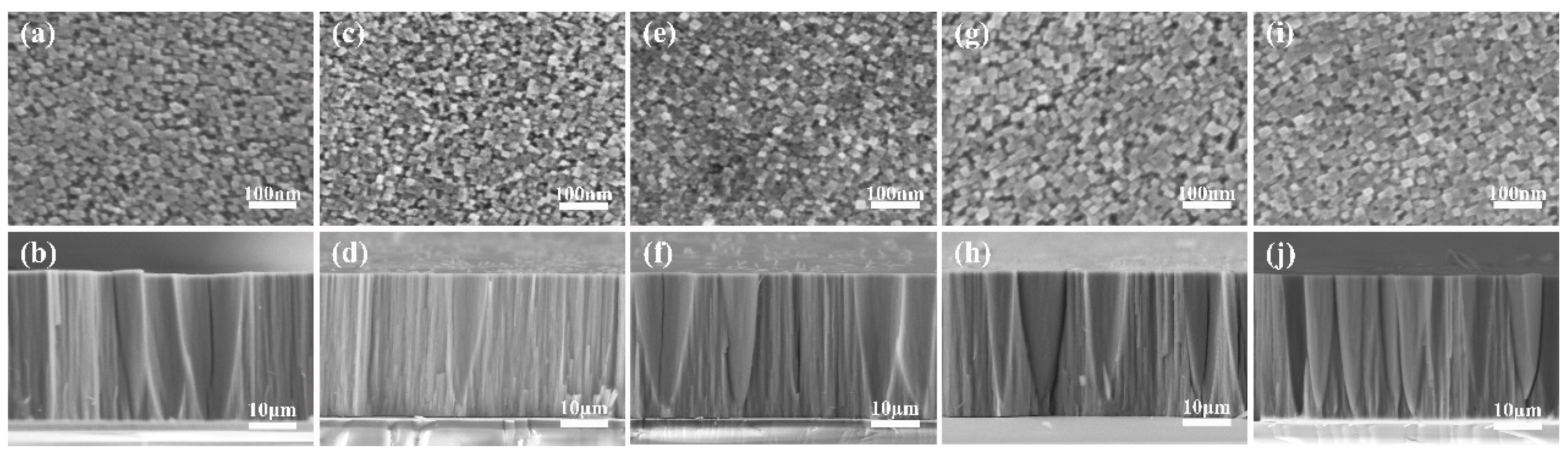
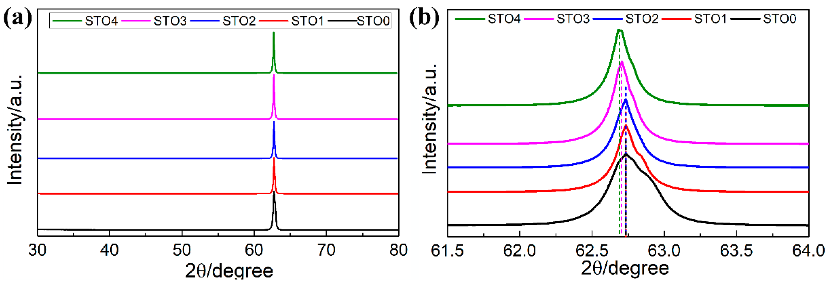
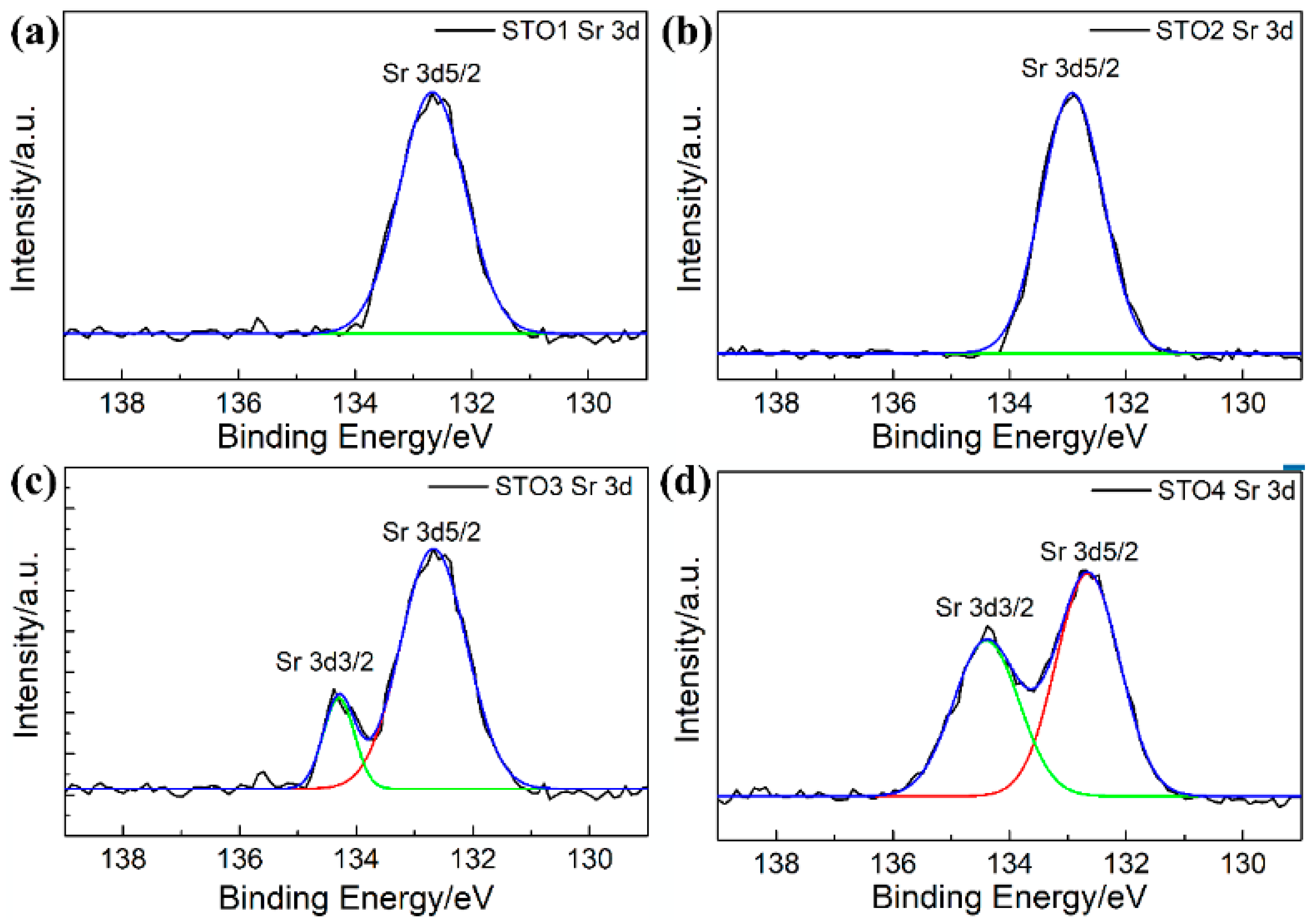
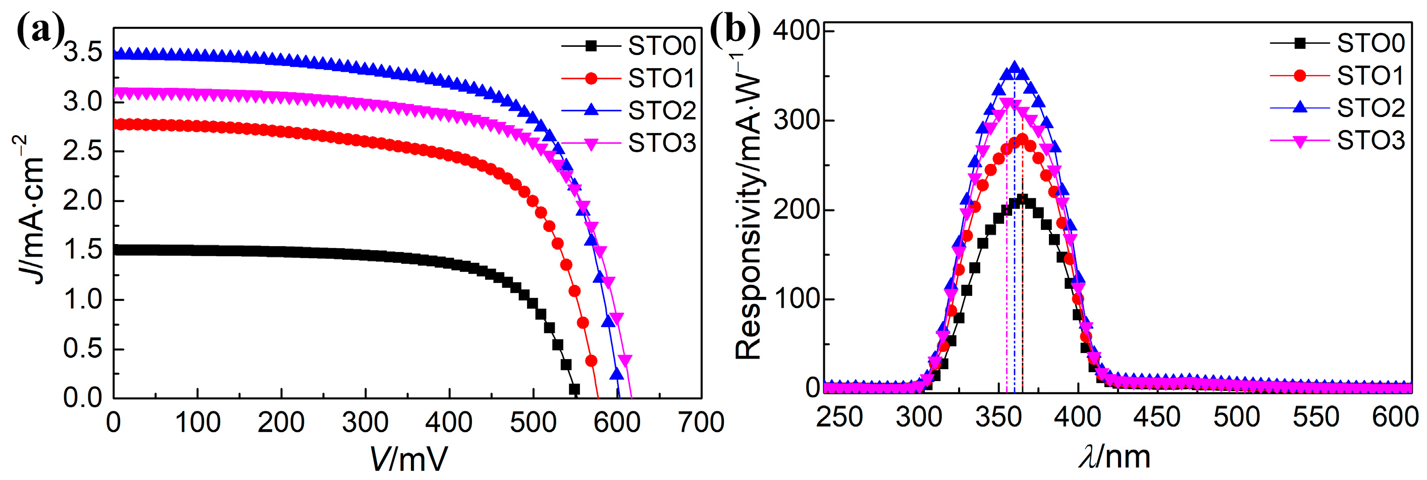
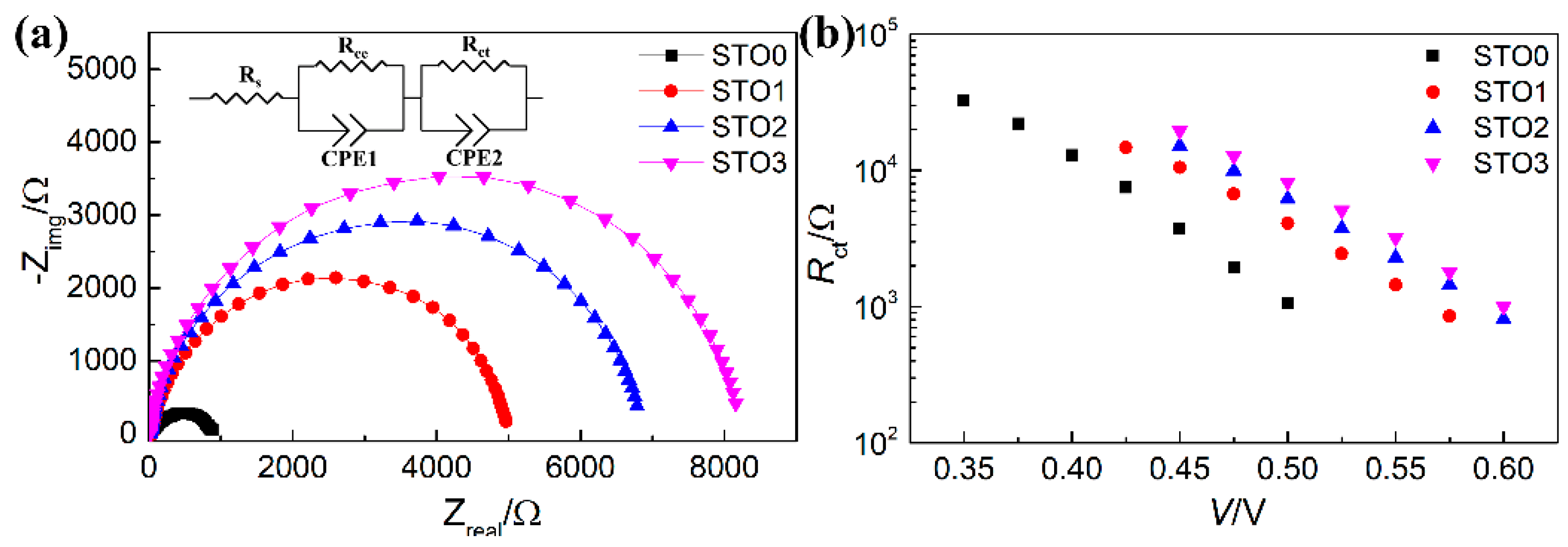
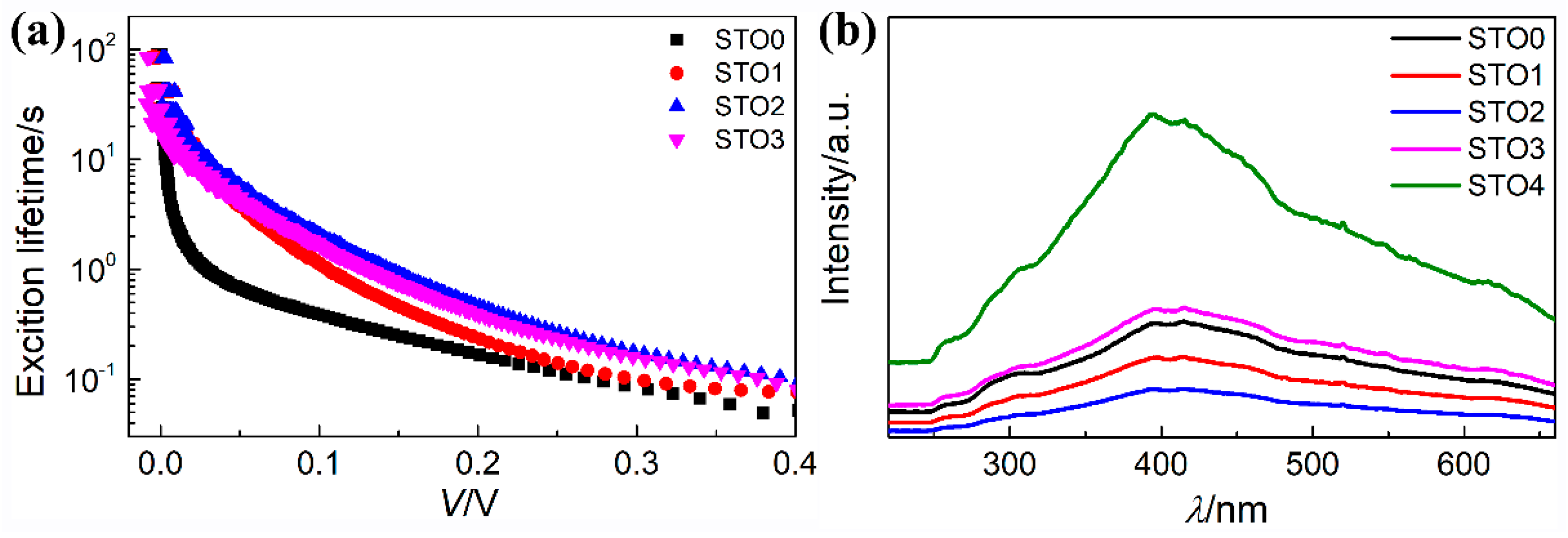
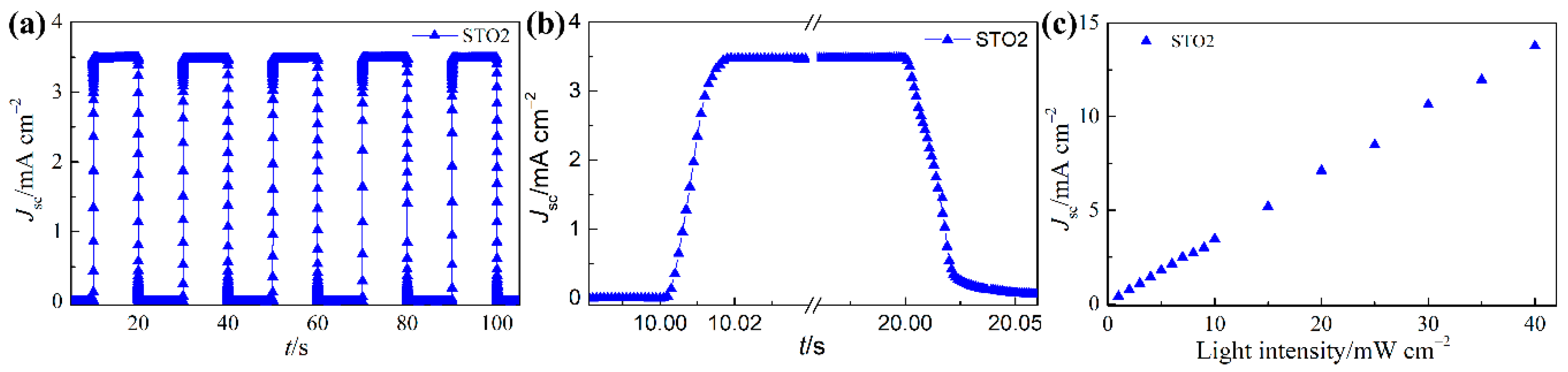
2. Results and Discussion

The experimental section is shown in Supplementary Data. The morphology of pure TiO2 and TiO2@SrTiO3 heterostructured nanowire arrays (STO0, STO1, STO2, STO3, and STO4) was characterized by field emission scanning electron microscope (FESEM), as shown in Figure 1. The top view of pure TiO2 NWAs, as shown in Figure 1a, illustrates that the cross section of nanowires is square with an average side length of 15 nm due to the tetragonal structure of the rutile TiO2, and the nanowire arrays exhibited regularly distribution. The cross-sectional FESEM image (Figure 1b) of STO0 shows that the nanowire arrays are perpendicular to the substrate with an approximate 33 μm thickness. Figure 1c–j indicate that the growth of SrTiO3 on the surface of TiO2 NWAs does not alter the diameter and thickness of TiO2 NWAs, which indicates that the growth of SrTiO3 happens in-situ on the surface of the TiO2 nanowire. To investigate the elemental distribution of TiO2@SrTiO3 heterostructures nanowire arrays, energy-dispersive X-ray spectroscopy (EDS) mapping characterization is employed (STO3 sample). Supplementary materials Figures S1 and S2 show the EDS elemental mapping images of the cross section and top surface of TiO2@SrTiO3 heterostructured nanowire arrays (STO3), respectively. Due to the homogeneous distribution of Sr element among the cross section and top surface of TiO2@SrTiO3 heterostructures nanowires, we can ensure that the formation of SrTiO3 happens on the surface of all TiO2 nanowires, so as to form TiO2@SrTiO3 heterostructure nanowires arrays.
To figure out the existential of the SrTiO3 coating layer, the detailed information regarding the microscopic structure of TiO2@SrTiO3 heterostructured nanowires (STO2) are exposed by transmission electron microscopy (TEM), as shown in Figure 2. The structure of TiO2@SrTiO3 heterostructured nanowire cluster is shown in the low magnification TEM image (Figure 2a), which indicated that the uniform nanowires, with a diameter of about 15 nm, constitute the nanowire cluster, as is consistent with the SEM results. The porous structure that each nanowire separates from the other makes for the immersion of the electrolyte. Figure 2b displays the high-resolution TEM (HRTEM) lattice image of a single TiO2@SrTiO3 heterostructured nanowire. The distinct lattice fringes differentiate TiO2 and SrTiO3 from the high-resolution TEM image. The obvious lattice spacing of 0.325 nm is in accordance with that of the (002) plane of rutile TiO2, indicating that the growth direction of rutile TiO2 NWs is along [001]. The interplanar spacing, with 0.272 nm, corresponds well to that of the (110) plane of cubic SrTiO3, which demonstrates the formation of a TiO2@SrTiO3 heterojunction structure. The SrTiO3coating layer is uniformly distributed and about 1.5 nm.
The X-ray diffraction (XRD) result of the as-prepared TiO2 nanowire arrays through hydrothermal treatment in PH 14 Sr(OH)2 aqueous solution with different treatment time (STO1, STO2, STO3, and STO4 samples). The crystalline structures and the state of Sr-doped of pure TiO2 and TiO2@SrTiO3 heterostructured nanowire arrays were investigated by X-ray diffraction (XRD) in the 2θ range of 30–80°. The XRD patterns of pure TiO2 (STO0) and TiO2@SrTiO3 heterostructured nanowire arrays (STO1, STO2, STO3, STO4) are shown in Figure 3a. For pure TiO2 nanowire arrays (STO0), the obvious diffraction peak that is located at 62.72° originates from the (002) plane of the tetragonal rutile phase TiO2 (JCPDS 21-1276), which should be attributed to the verticality of TiO2 nanowire arrays of highly [001] oriented growth and Fluorine-doped tin oxide (FTO) substrates. The XRD patterns did not show a distinctive peak of SrTiO3 phase, which might be due to the minor content of SrTiO3 as compared to TiO2, which can be effortlessly understood that the Bragg reflections that were indexed to SrTiO3 were not detected. There is something different that could be found in the magnification of XRD pattern of the (002) peak that was prepared at different treatment time, as shown in Figure 3b. It should be emphasized that, when the reaction time is short, the consistent location of (002) peaks of STO0, STO1, and STO2 suggest that no Sr element was doped into TiO2 lattice. When the treatment time is longer, the gradual shifting of the (002) peak occurred, which could be observed in the STO3 and STO4 samples. The shift of (002) peak location to a small angle suggests that the interplanar distance of (002) lattice plane augments due to the increase of treatment time. As the size of Sr2+ is larger than that of Ti4+, the augment of interplanar distance can be attributed to the replacement of Ti4+ by Sr2+. The state of Sr element doping into the lattice of TiO2 nanowire array can be further examined by the following X-ray photoelectron spectroscopy (XPS) techniques.
More specifics about the surface chemical state of TiO2@SrTiO3 heterostructured nanowire are explored by using XPS. From fully scanned spectrum (Figure S3a), the existence of Sr, Ti, O, and C in the TiO2@SrTiO3 heterostructured nanowire is confirmed. The peak of C 1s could be attributed to the carbon based impurity, and the binding energy for C 1s at 284.6 eV is applied as a criterion to calibrate the binding energies of the other elements [55]. The spectrum of the Ti 2p (Figure S3b) shows that the characteristic peak positions center at 458.28 eV related to Ti 2p3/2 and 463.98 eV related to Ti 2p1/2. The peak that is centered in 458.28 eV is comprised of TiO2 Ti 2p3/2 (458.6 eV) and SrTiO3 Ti 2p3/2 (457.8 eV), and the peak that is centered in 458.28 eV is comprised of TiO2 Ti 2p1/2 (464.4 eV) and SrTiO3 Ti 2p1/2 (463.5 eV) [56,57]. This could approve the formation of TiO2@SrTiO3 heterostructure. The XPS spectral peak of O 1s shows two small asymmetry peaks, (Figure S3c) one centered at 529.36 eV that should be linked with TiO2 and SrTiO3, meanwhile, the other peak that is centered at 531.08 eV is believed to be correlated with oxygen vacancy [58,59]. At the same time, a typical XPS fitted profile of Sr 3d is shown in Figure 4. The high resolution XPS spectrum of the Sr 3d region can be decomposed into two peaks of Sr 3d5/2 and Sr 3d3/2, which are centered at 132.74 and 134.47 eV, respectively. The peak at 132.74 eV is in accordance with those that were reported for perovskite SrTiO3, and the energy peak at 134.47 eV can be attributed to SrO complexes, which is attributed to the Sr element doping in the lattice of rutile TiO2 [60]. As shown in Figure 4a,b, when the reaction time is short, there is no peak in the high resolution XPS spectrum of the Sr 3d related to SrO, which means that no Sr element was doped into TiO2 nanowires. With the reaction time increasing, the energy peak that is related to SrO appeared, which means the Sr was doped into TiO2 nanowires, as shown in Figure 4c,d.
To evaluate the performance of the photoelectrochemical UVPDs based on STO0, STO1, STO2, and STO3 electrodes, the photocurrent-density (J) via voltage (V) characteristics were measured under a 10 mW·cm‒2 UV light source whose wavelength is 365 nm. A comparison of J-V characteristics of all UVPDs is shown in Figure 5a, and the J-V characteristics of UVPD based on STO4 is shown in Figure S4. The detailed data about the short-circuit photocurrent density (Jsc), the open-circuit photovoltage (Voc), fill factor (FF), and power conversion efficiency (η) are listed in Table 1. With the reaction time ranging from 0 to 60 min (STO0 to STO3), the Jsc first increases from 1.50 mA·cm−2 (STO0), to a maximum value of 3.48 mA·cm−2 (STO2), and then decreases with further increasing the treatment time. The Voc keeps an increasing trend with the increase of treatment time. The UVPDs that are based on STO0 show the lowest Voc due to the intrinsic property of TiO2 pure nanowires. The FF values that were obtained from the UVPDs show little change that suggests the growth of SrTiO3 do not destroy the well contact between pure TiO2 nanowires film and the FTO glass substrate. The power conversion efficiency (η) is the maximum of the product of photo current density and photo voltage, and FF could be calculated by the following equation: FF = η/(Jsc × Voc). The η displays the same trend with Jsc, which is enough to drive low-power-consuming complementary metal-oxide semiconductor (CMOS) circuits and certain nanodevices [61,62].
To pinpoint the cause of the Jsc variation, we tested the spectral photoresponsivity of the photoelectrochemical UVPDs based on STO0, STO1, STO2, and STO3. The relationship between the responsivity (defined as photocurrent per unit of incident optical power) and the incident light wavelength is shown in Figure 5b. As presented in Figure 5b, the incident light wavelength ranges from 250 to 600 nm at 0 bias. For the photoelectrochemical UVPD that is based on STO0, at 365 nm, the peak value of photoresponsivity is about 212 mA·W‒1, corresponding to the forbidden bandwidth of pure rutile TiO2. The FTO could absorbed the illumination whose wavelength is shorter than 300 nm, at the same time, photoresponsivity sharply reduces by about three orders of magnitude when the illumination whose wavelength is longer than 420 nm, which is proper for visual-blind ultraviolet detection application. For the photoelectrochemical UVPD that is based on TiO2@SrTiO3 heterostructured nanowire arrays (STO1, STO2, and STO3), the peak values of photoresponsivity are 279 at 365 nm, 358 at 360 nm, and 321 at 355 nm, respectively. The blue shift of the peak position may be due to that the forbidden bandwidth of SrTiO3 is larger than that of pure rutile TiO2. The variation tendency of photoresponsivity is consistent with the Jsc.
In fact, two factors that include the light harvesting efficiency and the rate of electron recombination mostly influence the photoresponsivity of the PEC UVPDs [63].
UV-vis diffuse reflectance spectra measurement was carried out to confirm the effect of the reaction time on the light harvesting efficiency. The thickness of nanowire arrays is too large, which meant that no light could pass through the nanowire arrays. The less reflection indicates more absorption. As displayed in Figure S5a, the variation the reflection of the pure TiO2 nanowire arrays (STO0) and TiO2@SrTiO3 heterostructured nanowire arrays (STO1, STO2, STO3, STO4) is regular. With the reaction time increasing, the absorption of samples enhances at a range of wavelengths from 300 to 400 nm. The equation for calculating the optical forbidden bandwidth from the diffuse reflectance is shown in Supplementary Information [64]. As shown in Figure S5b, the optical forbidden bandwidth of samples (STO0, STO1, STO2, STO3, STO4) with different reaction times is estimated to be 2.99, 3.02, 3.06, 3.09, and 2.95 eV, respectively. For the samples STO0, STO1, STO2, and STO3, the result of the optical forbidden bandwidth is consistent with the result of photoresponsivity, but for the sample with long reaction time (STO4), the doped Sr element into the crystal lattice of rutile TiO2 could create an impurity energy level and narrow the band gap [54], which accounts for the self-doping effect due to the bonding character of Ti–O–Sr [65]. Accordingly, the optical forbidden bandwidth is the result of the comprehensive effect of the SrTiO3 coating and doped Sr element. The distinct variation of the optical forbidden bandwidth also indicates that the amount of doped Sr element of STO4 obtained is larger than that of the sample STO3.
Electrochemical impedance spectroscopy (EIS) is applied at a bias of 0.5 V under dark condition to depict the photogenerated electron–hole pairs recombination dynamics at the photoanode/electrolyte interface to investigate the effect of the reaction time on the rate of electron recombination. Figure 6a displays the Nyquist plot curves of photoelectrochemical UVPDs that are based on STO0, STO1, STO2, and STO3. On the basis of the EIS model, in the Nyquist plot curve, the diameter of the obvious semicircle in the middle-frequency region, represents the charge transfer at the photoanode/electrolyte interface [66,67]. Accordingly, the diameter of the obvious semicircle increases with the reaction time augment, indicating that the possibility of the recombination of the photogenerated electrons and the redox in electrolyte decrease with the reaction time augment. This result is consistent with the variation tendency of photoresponsivity of photoelectrochemical UVPDs that are based on sample based on STO0, STO1, and STO2, but not with that of photoelectrochemical UVPDs that are based on sample based on STO3. Figure 6b shows plots of the interfacial charge recombination resistance as a function of the applied bias voltage, indicating the same results.
The dark current test was carried out to simply understand the photogenerated electrons recombination condition. Although the dark current is not direct data to provide the electron recombination rate, but lower dark current suggests lower photogenerated electrons recombination. As shown in Figure S6, at a same potential, the dark current of photoelectrochemical UVPD based on sample STO2 is the smallest among all of the UVPDs, which indicates that the rate of the recombination of photogenerated electrons is the smallest.
To identify the effect of reaction time on the photogenerated lifetime to understand the condition of photogenerated electron recombination open-circuit voltage decay (OCVD) more deeply, measurements of the UVPDs that were assembled with different photoanode were carried out. The OCVD technique has been commonly applied to examine the exciton electron lifetime (τe) and photogenerated electrons recombination problem in UVPDs [68,69,70]. The τe can be calculated from the corresponding OCVD curve of the UVPDs (as shown in Figure S7) and the calculation formula is also shown in Supplementary Information. Seeing that there is no current moving through the external circuit at open circle condition, the electrons must be reacted by I3 ions at the photoanode-electrolyte interface. Thus, the slow decay of Voc must be owed to the slow photogenerated electron recombination with the oxidation state of electrolyte on at the photoanode-electrolyte interface. The calculated τe as a function of Voc (in log-linear representation) is shown in Figure 7a. According to the previous research result [69,70,71,72], the τe value at a high voltage region mainly reflects the electron lifetime in the photoanodes. As illustrated in Figure 7a, the τe variation trend resembles the variation tendencies of photoresponsivity of photoelectrochemical UVPDs, which indicates that the photogenerated electrons are not only recombined with the redox in the electrolyte.
Due to the photogenerated carrier recombination being capable of leading to a noteworthy emission signal in the photoluminescence (PL) spectrum, the photogenerated charge carriers’ separation behavior of the photogenerated electron-hole pairs can be appraised by measurements of PL emission [73]. The PL intensity variation indicates the change of the recombination property of photogenerated electron-hole pairs in the photoanode. Figure 8 shows the PL spectra of pure TiO2 nanowire arrays (STO0) and TiO2@SrTiO3 heterostructured nanowire arrays (STO1, STO2, STO3, STO4). We could be informed that the reaction does not qualitatively change the shape of the PL emission, nevertheless, the PL intensity of the TiO2@SrTiO3 heterostructured nanowire arrays was found to be meaningfully varied when compared to that of the pure TiO2 nanowire arrays (STO0). After the TiO2@SrTiO3 heterostructure is formed, the intensity of PL peaks significantly decreases. The established energy barrier caused by the difference of the energy level of core-shell structures with type-II band alignment can help in the separation of the photogenerated electron-hole pairs and thus suppress interfacial charge recombination that decreases the probability of photogenerated carrier’s recombination in the photogenerated to produce photoluminescence. The obvious decrement of PL intensity can be attributed to the reduced recombination rate of photogenerated electron-hole pairs. With the further increasing of reaction time, the intensity of the PL peak regularly enhances. Doped Sr2+ elements could bring a defect of crystal lattice and recombination centers in the TiO2@SrTiO3 heterostructured nanowire arrays. At the same time, doped Sr2+ elements damage the carrier transport pathway that is built by the TiO2 nanowire. Both of these would bring out more recombination of photogenerated electron–hole pairs and then enhance the intensity of PL emission [54].
In common, evaluating the performance of UVPD from several perspectives, such as photoresponsivity, repeatability, stability, response speed, correlation between photocurrent and light intensity, and so on. To estimate the repeatability and stability of all UVPDs, time-dependent photocurrent signal is investigated under periodic pulse UV radiance with a luminous power density of 10 mW·cm−2, 20 s switching period, and 365 nm wavelength at zero bias, as shown in Figure 8a and Figure S8a. The cyclically regular switch of photocurrent signal from the “on” state to the “off” state indicates the ample repeatability and stability of this type of UVPDs. The sensitivity, also called on/off ratio, of the J signal can reach 28064 for the UVPD based on STO2, which is considerably higher than that (6276) of the UVPD that is based on STO0.
In common, the response speed was described by the rise time τr (the time to reach (1-1/e) of the maximum J) and decay time τd (the time for the photocurrent to drop to 1/e of its maximum J). Enlarged rising and decaying edges of the photocurrent response of all UVPDs are shown in Figure 8b and Figure S8b. the detailed data of τr and τd are listed in Table 2. We can find that the τr is very close to each other (11ms), but the τd of UVPD that is based on STO2 is the highest. In fact, the speed of recombination of photogenerated electron determines the magnitude of τd. In this experiment, the biggest factor that affects the speed of recombination of the photogenerated electron is that the photogenerated electron combines with the I3 in the electrolyte at the interface of the photoanode/electrolyte. From previous research in this manuscript, we can know that the recombination of photogenerated electron with the I3 in the electrolyte at the interface of photoanode/electrolyte is suppressed. Therefore, UVPD that is based on the STO2 sample achieves the longest decay time, although it presents the largest on/off ratio and photoresponsivity, which is consistent with the tendency of τe. To investigate the reaction between Jsc and the intensity of incident light, the Jsc as a function of the intensity of incident light of all UVPDs is presented in Figure 8c and Figure S8c. The Jsc measurements of UVPDs were measured under a 365 nm UV light source, whose light intensity varied from 1 to 40 mW·cm−2. Obviously, the Jsc shows an outstanding linear relationship with the growing intensity of incident light in a wide range. The slope of data is fitted through linear approximation by the least-square method, as shown in Figure S9. Moreover, the slope of Jsc and the intensity of incident light matches the Rλ that is attained from Figure 5c., suggesting that this type of photodetector is suitable in the precise measurement of intensity of UV irradiation.

3. Conclusions

In summary, Sr-doped free TiO2@SrTiO3 core-shell heterostructured nanowire arrays were successfully synthesized on FTO glass. We explored the effect of reaction time on the preparation of TiO2@SrTiO3 core-shell heterostructured nanowire arrays. When compared with pure TiO2 nanowire arrays, the photocurrent of UVPDs have been significantly enhanced after coating with SrTiO3. The UVPDs with a reaction time 40 min exhibited more excellent photoresponse properties than other TiO2@SrTiO3 heterostructured nanowire arrays that are based UVPDs. The electrochemical impedance spectroscopy results show that the formation of TiO2@SrTiO3 heterostructures can efficiently reduce the recombination at the interface of photoanode/electrolyte, and the photoluminescence results show the Sr doped enhance the recombination of photogenerated electron-hole pairs in the photoanode. Two effects dominate the performance of the UVPDs together. A large responsivity of 358 mA·W−1 was achieved at 360 nm for the UVPD based on Sr-doped free TiO2@SrTiO3 heterostructured nanowire arrays (reaction time is 40 min) without applied bias, together with the excellent on/off ratio of 28064. Additionally, this UVPD also exhibits fast response speed, excellent visible-blind characteristic, and linear optical signal response. Due to its operability in actual application, all of these manifest that this type of UV photodetector is a considerable selective candidate as next-generation UVPD.

Supplementary Materials

The following are available online at https://www.mdpi.com/2073-4352/9/3/134/s1, Experimental method, Figure S1: EDS elemental mapping images of cross section of TiO2@SrTiO3 heterostructured nanowire arrays (STO3), Figure S2: EDS elemental mapping images of top surface of TiO2@SrTiO3 heterostructured nanowire arrays (STO3), Figure S3: (a) XPS of TiO2@SrTiO3 heterostructure nanowire arrays (STO2), (b) XPS spectra of Ti 2p, and (c) XPS spectra of O 1s, Figure S4: JV characteristics a of the PEC UVPDs based on STO4, Figure S5: (a) The UV-vis diffusive reflectance spectra of samples STO0, STO1, STO2, STO3, STO4 and (b) the plots of transforming the Kubelka–Munk function versus the energy of light, Figure S6: Dark current density–voltage of all UVPDs (a) normal, (b) semi-logarithmic plots, Figure S7: Open-circuit voltage decay for all UVPDs and the UV intensity at first 10 s is 10 mA·cm−2, Figure S8: (a) Photocurrent responses, (b) The enlarged rising and decaying edges of the photocurrent response, and (c) J as a function of the incident UV light intensity from 1 to 40 mW·cm−2 of UVPDs based on STO0, STO1, STO2, STO3, Figure S9: Linear fitting of J as a function of the incident UV light intensity from 1 to 40 mW·cm−2 of UVPDs based on STO0, STO1, STO2, STO3.

Author Contributions

F.G. and D.W. designed the experiments; S.N. and B.W. performed the experiments; S.N., Y.Z., J.W. and S.J. analyzed the data; Y.Z., J.W. and S.J. contributed analysis tools; S.N. and D.W. wrote the paper, L.Z. coordinated the overall work.

Funding

This research was funded by the National Natural Science Foundation of China (Grant No. 51502061) and (Grant No. 61605036).

Conflicts of Interest

The authors declare no conflict of interest.

References

  1. Huang, Y.; Yu, Q.; Wang, J.; Wang, J.; Yu, C.; Abdalla, J.T.; Zeng, Z.; Jiao, S.; Wang, D.; Gao, S. Plasmon-Enhanced Self-Powered UV Photodetectors Assembled by Incorporating Ag@SiO2 Core−Shell Nanoparticles into TiO2 Nanocube Photoanodes. ACS Sustain. Chem. Eng. 2017, 6, 438–446. [Google Scholar] [CrossRef]
  2. Zhai, T.; Li, L.; Wang, X.; Fang, X.; Bando, Y.; Golberg, D. Recent Developments in One-Dimensional Inorganic Nanostructures for Photodetectors. Adv. Funct. Mater. 2010, 20, 4233–4248. [Google Scholar] [CrossRef]
  3. Prades, J.D.; Hernandez-Ramirez, F.; Jimenez-Diaz, R.; Manzanares, M.; Andreu, T.; Cirera, A.; Romano-Rodriguez, A.; Morante, J.R. The Effects of Electron-hole Separation on the Photoconductivity of Individual Metal Oxide Nanowires. Nanotechnology 2008, 19, 465501. [Google Scholar] [CrossRef] [PubMed]
  4. Li, L.; Gu, L.; Lou, Z.; Fan, Z.; Shen, G. ZnO Quantum Dots Decorated Zn2SnO4 Nanowire Heterojunction Photodetectors with Drastic Performance Enhancement and Flexible Ultraviolet Image Sensors. ACS Nano 2017, 11, 4067–4076. [Google Scholar] [CrossRef] [PubMed]
  5. Liu, Q.; Gong, M.; Cook, B.; Ewing, D.; Casper, M.; Stramel, A.; Wu, J. Fused Nanojunctions of Electron-Depleted ZnO Nanoparticles for Extraordinary Performance in Ultraviolet Detection. Adv. Mater. Interfaces 2017, 4, 1601064. [Google Scholar] [CrossRef]
  6. Yu, J.; Tian, N. High Spectrum Selectivity and Enhanced Responsivity of a ZnO Ultraviolet Photodetector Realized by the Addition of ZnO Nanoparticles Layer. Phys. Chem. Chem. Phys. 2016, 18, 24129–24133. [Google Scholar] [CrossRef] [PubMed]
  7. Jefferson, M. Sustainable energy development: Performance and prospects. Renew. Energy 2006, 31, 571–582. [Google Scholar] [CrossRef]
  8. Bie, Y.; Liao, Z.; Zhang, H.; Li, G.; Ye, Y.; Zhou, Y.; Xu, J.; Qin, Z.; Dai, L.; Yu, D. Self-Powered, Ultrafast, Visible-Blind UV Detection and Optical Logical Operation based on ZnO/GaN Nanoscale p-n Junctions. Adv. Mater. 2011, 23, 649–653. [Google Scholar] [CrossRef] [PubMed]
  9. Su, Y.; Lin, W.; Hsu, Y.; Wei, K. Conjugated Polymer/Nanocrystal Nanocomposites for Renewable Energy Applications in Photovoltaics and Photocatalysis. Small 2014, 10, 4427–4442. [Google Scholar] [CrossRef] [PubMed]
  10. Zhang, F.; Yuan, C.; Zhu, J.; Wang, J.; Zhang, X.; Lou, X. Flexible Films Derived from Electrospun Carbon Nanofibers Incorporated with Co3O4 Hollow Nanoparticles as Self-Supported Electrodes for Electrochemical Capacitors. Adv. Funct. Mater. 2013, 23, 3909–3915. [Google Scholar] [CrossRef]
  11. Fang, X.; Zhai, T.; Gautam, U.; Li, L.; Wu, L.; Bando, Y.; Golberg, D. ZnS Nanostructures: From Synthesis to Applications. Prog. Mater. Sci. 2011, 56, 175–287. [Google Scholar] [CrossRef]
  12. Hu, Y.; Zhang, Y.; Xu, C.; Zhu, G.; Wang, Z. High-output Nanogenerator by Rational Unipolar Assembly of Conical Nanowires and Its Application for Driving a Small Liquid Crystal Display. Nano Lett. 2012, 12, 5025–5031. [Google Scholar] [CrossRef] [PubMed]
  13. Han, J.; Fan, F.; Xu, C.; Lin, S.; Wei, M.; Duan, X.; Wang, Z. ZnO Nanotube-based Dye-sensitized Solar Cell and Its Application in Self-powered Devices. Nanotechnology 2010, 21, 405203. [Google Scholar] [CrossRef] [PubMed]
  14. Hu, Y.; Xu, C.; Zhang, Y.; Lin, L.; Snyder, R.; Wang, Z. A Nanogenerator for Energy Harvesting from a Rotating Tire and Its Application as a Self-powered Pressure/Speed Sensor. Adv. Mater. 2011, 23, 4068. [Google Scholar] [CrossRef] [PubMed]
  15. Zhang, H.; Yeung, K.; Robbins, J.; Pavlick, R.; Wu, M.; Liu, R.; Sen, A.; Phillips, S. Self-Powered Microscale Pumps Based on Analyte-Initiated Depolymerization Reactions. Angew. Chem. Int. Ed. 2012, 51, 2400–2454. [Google Scholar] [CrossRef] [PubMed]
  16. Yu, A.; Jiang, P.; Wang, Z. Nanogenerator as Self-powered Vibration Sensor. Nano Energy 2012, 1, 418–423. [Google Scholar] [CrossRef]
  17. Li, X.; Gao, C.; Duan, H.; Lu, B.; Pan, X.; Xie, E. Nanocrystalline TiO2 Film Based Photoelectrochemical Cell as Self-powered UV-photodetector. Nano Energy 2012, 1, 640–645. [Google Scholar] [CrossRef]
  18. Li, X.; Gao, C.; Duan, H.; Lu, B.; Wang, Y.; Chen, L.; Zhang, Z.; Pan, X.; Xie, E. High-performance Photoelectrochemical-type Self-powered UV Photodetector Using Epitaxial TiO2/SnO2 Branched Heterojunction Nanostructure. Small 2013, 9, 2005–2011. [Google Scholar] [CrossRef] [PubMed]
  19. Gao, C.; Li, X.; Wang, Y.; Chen, L.; Pan, X.; Zhang, Z.; Xie, E. Titanium Dioxide Coated Zinc Oxide Nanostrawberry Aggregates for Dye-sensitized Solar Cell and Self-powered UV-photodetector. J. Power Sources 2013, 239, 458–465. [Google Scholar] [CrossRef]
  20. Li, Q.; Wei, L.; Xie, Y.; Zhang, K.; Liu, L.; Zhu, D.; Jiao, J.; Chen, Y.; Yan, S.; Liu, G.; et al. ZnO Nanoneedle/H2O Solid-liquid Heterojunction-based Self-powered Ultraviolet Detector. Nanoscale Res. Lett. 2013, 8, 415. [Google Scholar] [CrossRef] [PubMed]
  21. Chen, L.; Li, X.; Wang, Y.; Gao, C.; Zhang, H.; Zhao, B.; Teng, F.; Zhou, J.; Zhang, Z.; Pan, X.; et al. Low-temperature Synthesis of Tin Dioxide Hollow Nanospheres and Their Potential Applications in Dye-sensitized Solar Cells and Photoelectrochemical Type Self-powered Ultraviolet Photodetectors. J. Power Sources 2014, 272, 886–894. [Google Scholar] [CrossRef]
  22. Xie, Y.; Wei, L.; Li, Q.; Chen, Y.; Liu, H.; Yan, S.; Jiao, J.; Liu, G.; Mei, L. A High Performance Quasi-solid-state Self-powered UV Photodetector Based on TiO2 Nanorod Arrays. Nanoscale 2014, 6, 9116–9121. [Google Scholar] [CrossRef] [PubMed]
  23. Li, H.; Jiao, S.; Li, H.; Li, L.; Zhang, X. Band-edge Modulated ZnO Pomegranates-on-paper Photodetector. J. Mater. Chem. C 2015, 3, 3702–3707. [Google Scholar] [CrossRef]
  24. Wang, X.; Dong, L.; Zhang, H.; Yu, R.; Pan, C.; Wang, Z. Recent Progress in Electronic Skin. Adv. Sci. 2015, 2, 1500169. [Google Scholar] [CrossRef] [PubMed] [Green Version]
  25. Chen, W.; Qiu, Y.; Yang, S. Branched ZnO Nanostructures as Building Blocks of Photoelectrodes for Efficient Solar Energy Conversion. Phys. Chem. Chem. Phys. 2012, 14, 10872–10881. [Google Scholar] [CrossRef] [PubMed]
  26. Crossland, E.; Noel, N.; Sivaram, V.; Leijtens, T.; Alexander-Webber, J.A.; Snaith, H.J. Mesoporous TiO2 Single Crystals Delivering Enhanced Mobility and Optoelectronic Device Performance. Nature 2013, 495, 215–219. [Google Scholar] [CrossRef] [PubMed]
  27. Jiang, Y.; Zhang, W.; Jie, J.; Meng, X.; Fan, X.; Lee, S. Photoresponse Properties of CdSe Single-Nanoribbon Photodetectors. Adv. Funct. Mater. 2007, 17, 1795–1800. [Google Scholar] [CrossRef]
  28. Jie, J.; Zhang, W.; Jiang, Y.; Meng, X.; Li, Y.; Lee, S. Photoconductive Characteristics of Single-crystal CdS Nanoribbons. Nano Lett. 2006, 6, 1887–1892. [Google Scholar] [CrossRef] [PubMed]
  29. Luo, L.; Yang, X.; Liang, F.; Jie, J.; Li, Q.; Zhu, Z.; Wu, C.; Yu, Y.; Wang, L. Transparent and Flexible Selenium Nanobelt-based Visible Light Photodetector. CrystEngComm 2012, 14, 1942–1947. [Google Scholar] [CrossRef]
  30. Zhai, T.; Li, L.; Ma, Y.; Liao, M.; Wang, X.; Fang, X.; Yao, J.; Bando, Y.; Golberg, D. One-dimensional Inorganic Nanostructures: Synthesis, Field-emission and Photodetection. Chem. Soc. Rev. 2011, 40, 2986–3004. [Google Scholar] [CrossRef] [PubMed]
  31. Dasgupta, N.; Sun, J.; Liu, C.; Brittman, S.; Andrews, S.; Lim, J.; Gao, H.; Yan, R.; Yang, P. 25th Anniversary Article: Semiconductor Nanowires-synthesis, Characterization, and Applications. Adv. Mater. 2014, 26, 2137–2184. [Google Scholar] [CrossRef] [PubMed]
  32. Barth, S.; Hernandez-Ramirez, F.; Holmes, J.; Romano-Rodriguez, A. Synthesis and Applications of One-dimensional Semiconductors. Prog. Mater. Sci. 2010, 55, 563–627. [Google Scholar] [CrossRef]
  33. Guo, P.; Jiang, J.; Shen, S.; Guo, L. ZnS/ZnO Heterojunction as Photoelectrode: Type II Band Alignment towards Enhanced Photoelectrochemical Performance. Int. J. Hydrogen Energy 2013, 38, 13097–13103. [Google Scholar] [CrossRef]
  34. Grätzel, M. Photoelectrochemical Cells. Nature 2001, 414, 338–344. [Google Scholar] [CrossRef] [PubMed]
  35. Tiwana, P.; Docampo, P.; Johnston, M.B.; Snaith, H.J.; Herz, L.M. Electron Mobility and Injection Dynamics in Mesoporous ZnO, SnO2, and TiO2 Films Used in Dye-sensitized Solar Cells. ACS Nano 2011, 5, 5158–5166. [Google Scholar] [CrossRef] [PubMed]
  36. Yang, S.; Hou, Y.; Xing, J.; Zhang, B.; Tian, F.; Yang, X.H.; Yang, H.G. Ultrathin SnO2 Scaffolds for TiO2-Based Heterojunction Photoanodes in Dye-Sensitized Solar Cells: Oriented Charge Transport and Improved Light Scattering. Chem. Eur. J. 2013, 19, 9366–9370. [Google Scholar] [CrossRef] [PubMed]
  37. Xue, H.; Kong, X.; Liu, Z.; Liu, C.; Zhou, J.; Chen, W.; Ruan, S.; Xu, Q. TiO2 Based Metal-Semiconductor-Metal Ultraviolet Photodetectors. Appl. Phys. Lett. 2007, 90, 201118. [Google Scholar] [CrossRef]
  38. Xie, Y.; Wei, L.; Li, Q.; Chen, Y.; Yan, S.; Jiao, J.; Liu, G.; Mei, L. High-performance Self-powered UV Photodetectors Based on TiO2 Nano-branched Arrays. Nanotechnology 2014, 25, 075202. [Google Scholar] [CrossRef] [PubMed]
  39. Xie, Y.; Wei, L.; Wei, G.; Li, Q.; Wang, D.; Chen, Y.; Yan, S.; Liu, G.; Mei, L.; Jiao, J. A Self-powered UV Photodetector Based on TiO2 Nanorod Arrays. Nanoscale Res. Lett. 2013, 8, 188. [Google Scholar] [CrossRef] [PubMed]
  40. Cao, C.; Hu, C.; Wang, X.; Wang, S.; Tian, Y.; Zhang, H. UV Sensor Based on TiO2 Nanorod Arrays on FTO Thin Film. Sens. Actuators B Chem. 2011, 156, 114–119. [Google Scholar] [CrossRef]
  41. Wang, Y.; Han, W.; Zhao, B.; Chen, L.; Teng, F.; Li, X.; Gao, C.; Zhou, J.; Xie, E. Performance Optimization of Self-powered Ultraviolet Detectors Based on Photoelectrochemical Reaction by Utilizing Dendriform Titanium Dioxide Nanowires as Photoanode. Sol. Energy Mater. Sol. C 2015, 140, 376–381. [Google Scholar] [CrossRef]
  42. Li, Y.; Yu, H.; Song, W.; Li, G.; Yi, B.; Shao, Z. A Novel Photoelectrochemical Cell with Self-organized TiO2 Nanotubes as Photoanodes for Hydrogen Generation. Int. J. Hydrogen Energy 2011, 36, 14374–14380. [Google Scholar] [CrossRef]
  43. Zhou, J.; Chen, L.; Wang, Y.; He, Y.; Pan, X.; Xie, E. An Overview on Emerging Photoelectrochemical Self-powered Ultraviolet Photodetectors. Nanoscale 2016, 8, 50–73. [Google Scholar] [CrossRef] [PubMed]
  44. Zhang, Q.; Cao, G. Nanostructured Photoelectrodes for Dye-sensitized Solar Cells. Nano Today 2011, 6, 91–109. [Google Scholar] [CrossRef]
  45. Liu, G.; Kong, L.; Yan, J.; Liu, Z.; Zhang, H.; Lei, P.; Xu, T.; Mao, H.; Chen, B. Nanocrystals in compression: Unexpected structural phase transition and amorphization due to surface impurities. Nanoscale 2016, 8, 11803–11809. [Google Scholar] [CrossRef] [PubMed]
  46. Cao, J.; Zhou, J.; Zhang, Y.; Wang, Y.; Liu, X. Dominating Role of Aligned MoS2/Ni3S2 Nanoarrays Supported on Three-Dimensional Ni Foam with Hydrophilic Interface for Highly Enhanced Hydrogen Evolution Reaction. ACS Appl. Mater. Interfaces 2018, 10, 1752–1760. [Google Scholar] [CrossRef] [PubMed]
  47. Ni, S.; Guo, F.; Wang, D.; Liu, G.; Xu, Z.; Kong, L.; Wang, J.; Jiao, S.; Zhang, Y.; Yu, Q.; et al. Effect of MgO Surface Modification on the TiO2 Nanowires Electrode for Self-Powered UV Photodetectors. ACS Sustain. Chem. Eng. 2018, 6, 7265–7272. [Google Scholar] [CrossRef]
  48. Wu, Z.; Wang, Y.; Sun, L.; Mao, Y.; Wang, M.; Lina, C. An Ultrasound-Assisted Deposition of NiO Nanoparticles on TiO2 Nanotube Arrays for Enhanced Photocatalytic Activity. J. Mater. Chem. A 2014, 2, 8223–8229. [Google Scholar] [CrossRef]
  49. Zhang, M.; Yang, C.; Pu, W.; Tan, Y.; Yang, K.; Zhang, J. Liquid Phase Deposition of WO3/TiO2 Heterojunction Films with High Photoelectrocatalytic Activity under Visible Light Irradiation. Electrochim. Acta 2014, 148, 180–186. [Google Scholar] [CrossRef]
  50. Grönqvist, J.; Søndergaard, N.; Boxberg, F.; Guhr, T.; Åberg, S.; Xu, H. Strain in Semiconductor Core-shell Nanowires. J. Appl. Phys. 2009, 106, 53508. [Google Scholar] [CrossRef]
  51. Søndergaard, N.; He, Y.; Fan, C.; Han, R.; Guhr, T.; Xu, H. Strain Distributions in Lattice-mismatched Semiconductor Core-shell Nanowires. J. Vac. Sci. Technol. B 2009, 27, 827–830. [Google Scholar] [CrossRef]
  52. Boxberg, F.; Søndergaard, N.; Xu, H. Photovoltaics with Piezoelectric Core-shell Nanowires. Nano Lett. 2010, 10, 1108–1112. [Google Scholar] [CrossRef] [PubMed]
  53. Wang, Z. Progress in Piezotronics and Piezo-phototronics. Adv. Mater. 2012, 24, 4632–4646. [Google Scholar] [CrossRef] [PubMed]
  54. Baker, D.; Kamat, P.V. Photosensitization of TiO2 Nanostructures with CdS Quantum Dots: Particulate Versus Tubular Support Architectures. Adv. Funct. Mater. 2009, 19, 805–811. [Google Scholar] [CrossRef]
  55. Zhang, J.; Jiao, S.; Wan, Y.; Gao, S.; Wang, D.; Wang, J. A Well-grown β-Ga2O3 Microrod Array Formed from GaOOH on a Si (100) Substrate and Growth Mechanism Study. CrystEngComm 2018, 20, 4329–4335. [Google Scholar] [CrossRef]
  56. Sanjines, R.; Tang, H.; Berger, H.; Gozzo, F.; Margaritondo, G.; Levy, F. Electronic Structure of Anatase TiO2 Oxide. J. Appl. Phys. 1994, 75, 2945–2951. [Google Scholar] [CrossRef]
  57. Aas, N.; Pringle, T.; Bowker, M. Adsorption and Decomposition of Methanol on TiO2, SrTiO3 and SrO. J. Chem. Soc. Faraday Trans. 1994, 90, 1015–1022. [Google Scholar] [CrossRef]
  58. Bai, H.; Liu, Z.; Sun, D. Hierarchical ZnO/Cu “Corn-like” Materials with High Photodegradation and Antibacterial Capability under Visible Light. Phys. Chem. Chem. Phys. 2011, 13, 6205–6210. [Google Scholar] [CrossRef] [PubMed]
  59. Yang, W. X-ray Photoelectron Spectroscopy and Electrical Properties Studies of La2O3-doped Strontium Titanate Ceramics Prepared by Sol-precipitation Method. J. Mater. Sci. 1999, 34, 3533–3544. [Google Scholar] [CrossRef]
  60. Cao, T.; Li, Y.; Wang, C.; Shao, C.; Liu, Y. A Facile in situ Hydrothermal Method to SrTiO3/TiO2 Nanofiber Heterostructures with High Photocatalytic Activity. Langmuir 2011, 27, 2946–2952. [Google Scholar] [CrossRef] [PubMed]
  61. Pan, C.; Wu, H.; Wang, C.; Wang, B.; Zhang, L.; Cheng, Z.; Hu, P.; Pan, W.; Zhou, Z.; Yang, X.; et al. Nanowire-Based High-Performance “Micro Fuel Cells”: One Nanowire, One Fuel Cell. Adv. Mater. 2008, 20, 1644–1648. [Google Scholar] [CrossRef]
  62. Harrison, R.; Koch, C. A Robust Analog VLSI Reichardt Motion Sensor. Analog Integr. Circ. Signal Proc. 2000, 24, 213–229. [Google Scholar] [CrossRef]
  63. Zhou, Z.; Fan, J.; Wang, X.; Zhou, W.; Du, Z.; Wu, S. Effect of Highly Ordered Single-crystalline TiO2 Nanowire Length on the Photovoltaic Performance of Dye-sensitized Solar Cells. ACS Appl. Mater. Interfaces 2011, 3, 4349–4353. [Google Scholar] [CrossRef] [PubMed]
  64. Hamedani, H.; Allam, N.; Garmestani, H.; ElSayed, M. Electrochemical Fabrication of Strontium-doped TiO2 Nanotube Array Electrodes and Investigation of Their Photoelectrochemical Properties. J. Phys. Chem. C 2011, 115, 13480–13486. [Google Scholar] [CrossRef]
  65. Zhang, C.; Chen, S.; Mo, L.; Huang, Y.; Tian, H.; Hu, L.; Huo, Z.; Dai, S.; Kong, F.; Pan, X. Charge Recombination and Band-edge Shift in the Dye-sensitized Mg2+-doped TiO2 Solar Cells. J. Phys. Chem. C 2011, 115, 16418–16424. [Google Scholar] [CrossRef]
  66. Kim, C.; Suh, S.; Choi, M.; Kang, Y.; Kang, Y. Fabrication of SrTiO3-TiO2 Heterojunction Photoanode with Enlarged Pore Diameter for Dye-sensitized Solar Cells. J. Mater. Chem. A 2013, 1, 11820–11827. [Google Scholar] [CrossRef]
  67. Sun, H.; Pan, L.; Piao, X.; Sun, Z. Long Afterglow SrAl2O4:Eu,Dy Phosphors for CdS Quantum Dot-sensitized Solar Cells with Enhanced Photovoltaic Performance. J. Mater. Chem. A 2013, 1, 6388–6392. [Google Scholar] [CrossRef]
  68. Zaban, A.; Greenshtein, M.; Bisquert, J. Determination of the Electron Lifetime in Nanocrystalline Dye Solar Cells by Open-Circuit Voltage Decay Measurements. ChemPhysChem 2003, 4, 859–864. [Google Scholar] [CrossRef] [PubMed]
  69. Bisquert, J.; Zaban, A.; Greenshtein, M.; Mora-Sero, I. Determination of Rate Constants for Charge Transfer and the Distribution of Semiconductor and Electrolyte Electronic Energy Levels in Dye-sensitized Solar Cells by Open-circuit Photovoltage Decay Method. J. Am. Chem. Soc. 2004, 126, 13550–13559. [Google Scholar] [CrossRef] [PubMed]
  70. Liu, Y.; Sun, X.; Tai, Q.; Hu, H.; Chen, B.; Huang, N.; Sebo, B.; Zhao, X. Efficiency Enhancement in Dye-sensitized Solar Cells by Interfacial Modification of Conducting Glass/Mesoporous TiO2 Using a Novel ZnO Compact Blocking Film. J. Power Sources 2011, 196, 475–481. [Google Scholar] [CrossRef]
  71. Liu, G.; Kong, L.; Gong, J.; Yang, W.; Mao, H.; Hu, Q.; Liu, Z.; Schaller, R.D.; Zhang, D.; Xu, T. Pressure-Induced Bandgap Optimization in Lead-Based Perovskites with Prolonged Carrier Lifetime and Ambient Retainability. Adv. Func. Mater. 2017, 27, 1604208. [Google Scholar] [CrossRef]
  72. Kong, L.; Liu, G.; Gong, J.; Hu, Q.; Schaller, R.D.; Dera, P.; Zhang, D.; Liu, Z.; Yang, W.; Zhu, K.; et al. Simultaneous band-gap narrowing and carrier-lifetime prolongation of organic–inorganic trihalide perovskites. Proc. Natl. Acad. Sci. USA 2016, 113, 8910–8915. [Google Scholar] [CrossRef] [PubMed] [Green Version]
  73. Tang, R.; Yin, L. Enhanced Photovoltaic Performance of Dye-sensitized Solar Cells Based on Sr-doped TiO2/SrTiO3 Nanorod Array Heterostructures. J. Mater. Chem. A 2015, 3, 17417–17425. [Google Scholar] [CrossRef]
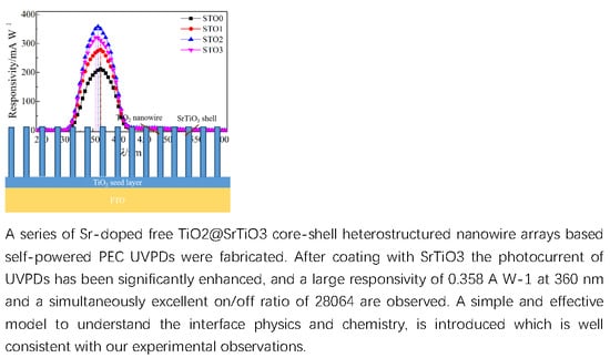
Figure 1. Morphological characterizations of the smooth-surface and rough-surface TiO2 NWAs: (a,c,e,g,i) top-surface FESEM image of STO0, STO1, STO2, STO3, STO4, respectively; and (b,d,f,h,j) cross-sectional FESEM image of STO0, STO1, STO2, STO3, STO4, respectively.
Crystals 09 00134 g001
Figure 2. (a) TEM image of nanowire bundles; (b) HRTEM image of a single TiO2@SrTiO3 heterostructured nanowire.
Crystals 09 00134 g002
Figure 3. (a) X-ray diffraction (XRD) patterns of pure TiO2 (STO0) and TiO2@SrTiO3 heterostructured nanowire arrays, (b) the enlarged X-ray diffraction (XRD) patterns between 61.5° and 64.0°.
Crystals 09 00134 g003
Figure 4. X-ray photoelectron spectroscopy (XPS) spectra of Sr 3d of TiO2@SrTiO3 heterostructured nanowire arrays: (a) STO1, (b) STO2, (c) STO3, (d) STO4.
Crystals 09 00134 g004
Figure 5. (a) J-V characteristics and (b) the spectral photoresponsivity of the photoelectrochemical ultraviolet photodetectors (PEC UVPDs) based on STO0, STO1, STO2, and STO3.
Crystals 09 00134 g005
Figure 6. (a) Electrochemical impedance spectra of UVPDs based on STO0, STO1, STO2, and STO3 measured at 0.5 V bias voltage in dark condition (b) Plots of the inter- facial charge recombination resistance as a function of the applied bias voltage.
Crystals 09 00134 g006
Figure 7. (a) the τe (in log-linear representation) as a function of open-circuit voltage, (b) the photoluminescence (PL) spectra measured at room temperature of all samples on FTO substrates.
Crystals 09 00134 g007
Figure 8. (a) Photocurrent responses, (b) The enlarged rising and decaying edges of the photocurrent response, and (c) J as a function of the incident UV light intensity from 1 to 40 mW·cm‒2 of UVPD based on STO2.
Crystals 09 00134 g008
Table 1. Detailed data of short-circuit photocurrent density (Jsc), open-circuit photovoltage (Voc), fill factor (FF), power conversion efficiency (η), and photoresponsivity of all UVPDs.
SampleJsc (mA·cm−2)Voc (mV)FF (%)η (%)Photoresponsivity (mA·W−1)
STO01.5055268.10.566212 at 365 nm
STO12.7757767.91.045279 at 365 nm
STO23.4860267.71.418358 at 360 nm
STO33.1161667.61.294321 at 355 nm
Table 2. Dark current, on/off ratio, τr and τd of UVPDs based on STO0, STO1, STO2, STO3.
SampleDark Current (mA·cm−2)On/Off Ratioτr (ms)τd (ms)
STO02.39 × 10−462761012
STO11.53 × 10−4181041113
STO21.24 × 10−4280641115
STO31.36 × 10−4228671114

