Property Improvement of GaAs Surface by 1-Octadecanethiol Passivation


Abstract
:1. Introduction
2. Experiment
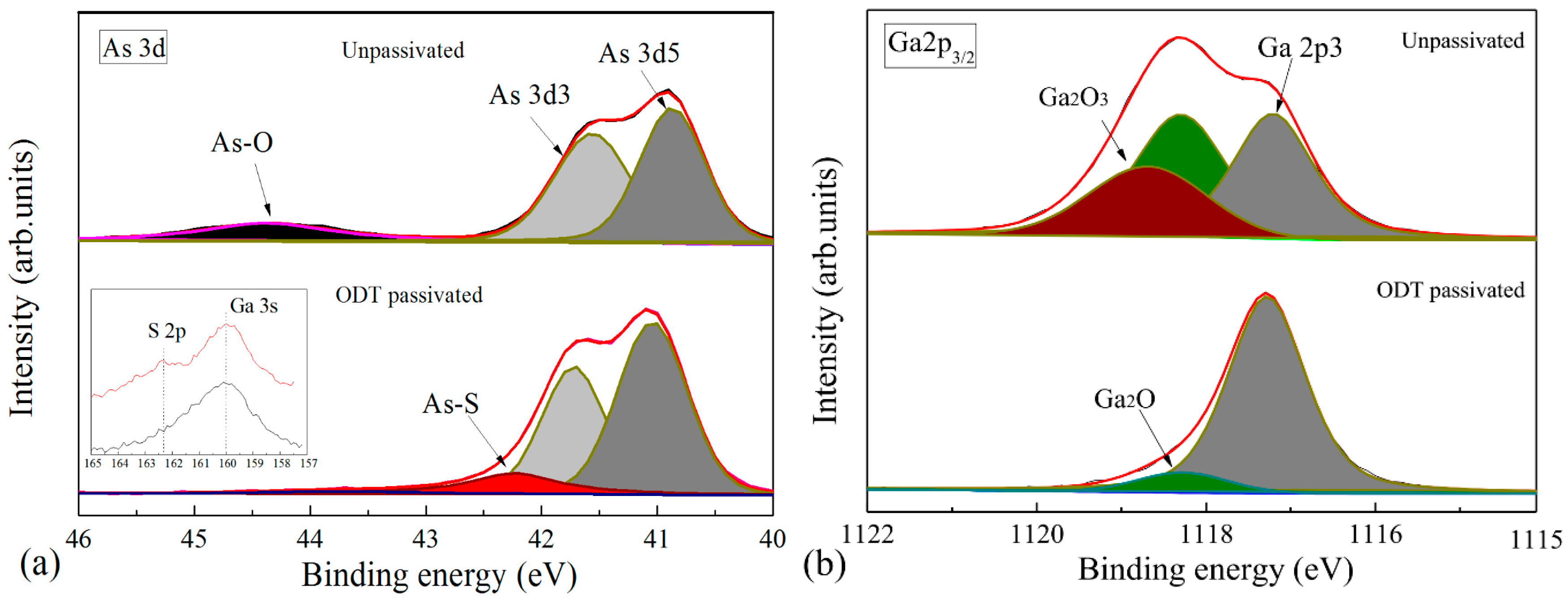
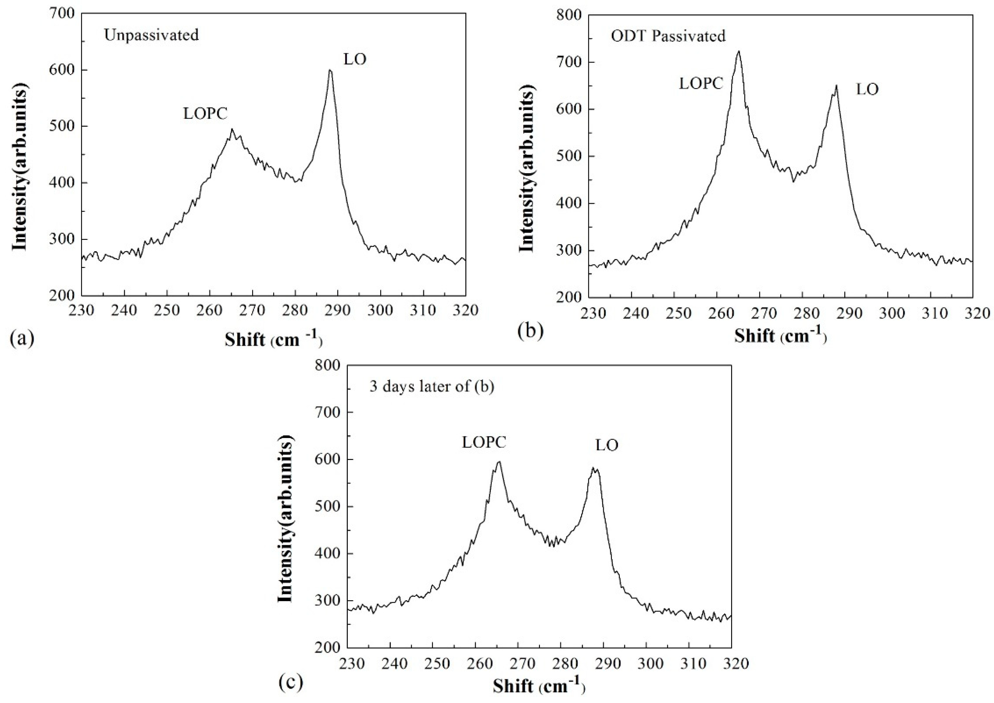
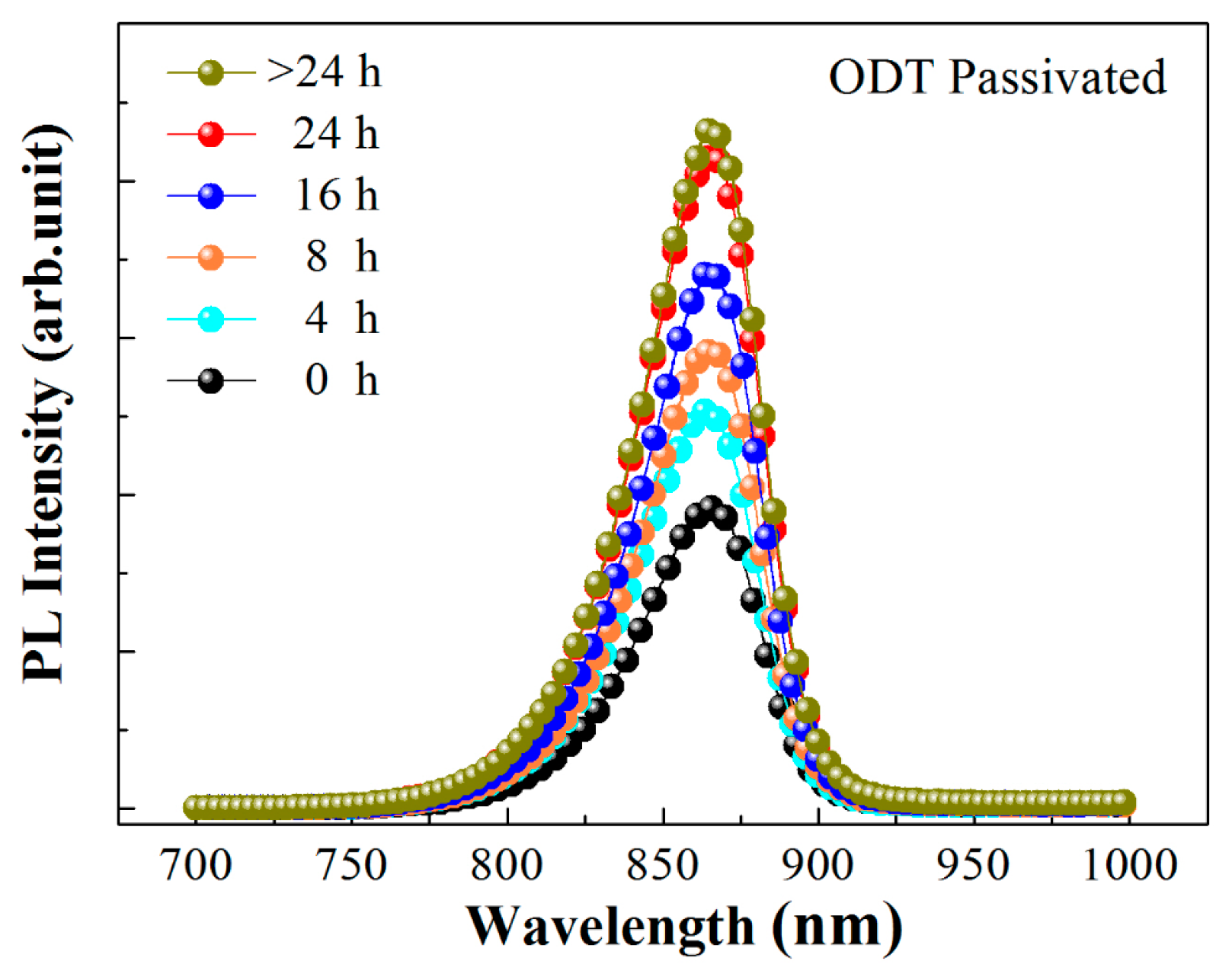
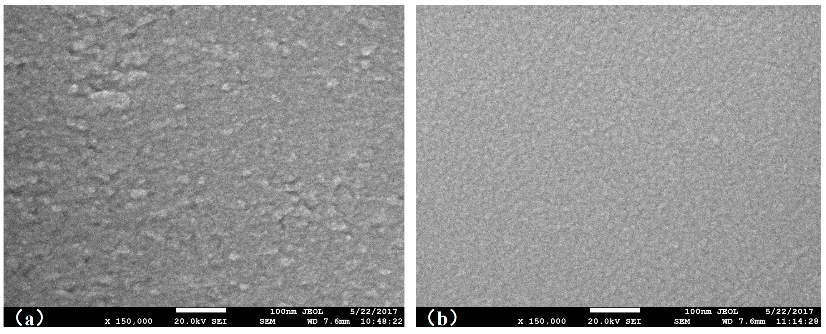
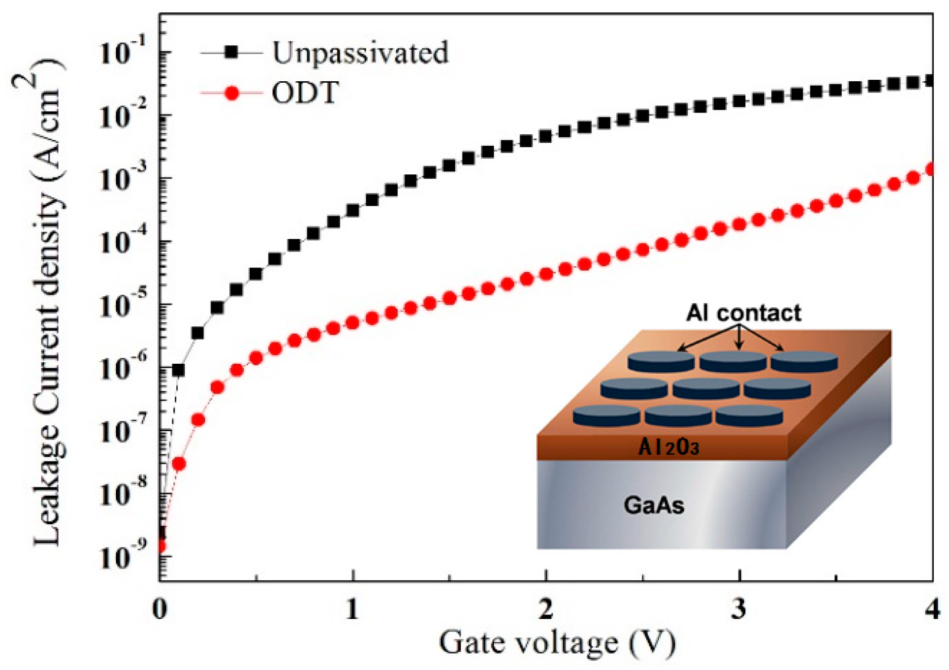
3. Discussion
4. Conclusions
Author Contributions
Funding
Conflicts of Interest
References
- Zhou, L.; Gao, X.; Wang, Y.; Xu, L.; Jia, B.; Bai, D.; Bo, B. Facet passivation of GaAs based LDs by plasma pretreatment and RF sputtered AlN film coating. J. Lightw. Technol. 2013, 31, 2279–2283. [Google Scholar]
- Xu, Y.; Gao, X.; Zhang, X.; Qiao, Z.; Zhang, J.; Zhou, L.; Bo, B. Effects on the surface and luminescence properties of GaAs by SF6 plasma passivation. Crystals 2018, 8, 339. [Google Scholar] [CrossRef]
- Robertson, J.; Guo, Y.; Lin, L. Defect state passivation at III-V oxide interfaces for complementary metal–oxide–semiconductor devices. J. Appl. Phys. 2015, 117, 112806. [Google Scholar] [CrossRef]
- Hinkle, C.L.; Milojevic, M.; Brennan, B.; Sonnet, A.M.; Aguirre-Tostado, F.S.; Hughes, G.J.; Vogel, E.M.; Wallace, R.M. Detection of Ga suboxides and their impact on III-V passivation and fermi-level pinning. Appl. Phys. Lett. 2009, 94, 162101. [Google Scholar] [CrossRef]
- Tajik, N.; Peng, Z.; Kuyanov, P.; LaPierre, R.R. Sulfur passivation and contact methods for GaAs nanowire solar cells. Nanotechnology 2011, 22, 225402. [Google Scholar] [CrossRef] [PubMed]
- Lebedev, M.V.; Kunitsyna, E.V.; Calvet, W.; Mayer, T.; Jaegermann, W. Sulfur passivation of GaSb (100) surfaces: Comparison of aqueous and alcoholic sulfide solutions using synchrotron radiation photoemission spectroscopy. J. Phys. Chem. 2013, 117, 15996–16004. [Google Scholar] [CrossRef]
- Ghita, R.V.; Negrila, C.C.; Cotirlan, C.; Logofatu, C. On the passivation of GaAs surface by sulfide compounds. Dig. J Nanomater. Biostruct. 2013, 8, 10. [Google Scholar]
- Lucero, A.T.; Byun, Y.-C.; Qin, X.; Cheng, L.; Kim, H.; Wallace, R.M.; Kim, J. Formation of a ZnO/ZnS interface passivation layer on (NH4)2S treated In0.53Ga0.47As: Electrical and in-situ X-ray photoelectron spectroscopy characterization. Jpn. J. Appl. Phys. 2016, 55, 08PC02. [Google Scholar] [CrossRef]
- Contreras, Y.; Mancheno-Posso, P.; Muscat, A.J. Comparison of the chemical passivation of GaAs, In0.53Ga0.47As, and insb with 1-eicosanethiol. Sol. State Phenom. 2016, 255, 55–60. [Google Scholar] [CrossRef]
- Budz, H.A.; LaPierre, R.R. Properties of octadecanethiol self-assembled monolayers deposited on GaAs from liquid and vapor phases. J. Vac. Sci. Technol. Vac. Surf. Films 2008, 26, 1425–1431. [Google Scholar] [CrossRef]
- Budz, H.A.; Biesinger, M.C.; LaPierre, R.R. Passivation of GaAs by octadecanethiol self-assembled monolayers deposited from liquid and vapor phases. J. Vac. Sci. Technol. Microelectron. Nanometer Struct. 2009, 27, 637. [Google Scholar] [CrossRef]
- Ye, S.; Li, G.; Noda, H.; Uosaki, K.; Osawa, M. Characterization of self-assembled monolayers of alkanethiol on GaAs surface by contact angle and angle-resolved XPS measurements. Surf. Sci. 2003, 529, 163–170. [Google Scholar] [CrossRef]
- Mancheno-Posso, P.; Muscat, A.J. Self-assembly of alkanethiolates directs sulfur bonding with GaAs (100). Appl. Surf. Sci. 2017, 397, 1–12. [Google Scholar] [CrossRef]
- Cuypers, D.; Fleischmann, C.; Van Dorp, D.H.; Brizzi, S.; Tallarida, M.; Müller, M.; Hönicke, P.; Billen, A.; Chintala, R.; Conard, T.; et al. Sacrificial self-assembled monolayers for the passivation of GaAs (100) surfaces and interfaces. Chem. Mater. 2016, 28, 5689–5701. [Google Scholar] [CrossRef]
- Vasily, N.; Bessolov, M.V.L.; Ivankov, A.F.; Bauhofer, W.; Dietrich, R.T.Z. Electronic properties of GaAs (100) surface passivated in alcoholic sulfide solutions. Appl. Surf. Sci. 1993, 133, 17–24. [Google Scholar]
- Dorsten, J.F.; Maslar, J.E.; Bohn, P.W. Near-surface electronic structure in GaAs (100) modified with self-assembled monolayers of octadecylthiol. Appl. Phys. Lett. 1995, 66, 1755–1757. [Google Scholar] [CrossRef]
- Wang, J.; Liu, X.H.; Li, Z.S.; Su, R.Z.; Ling, Z.; Cai, W.Z.; Hou, X.Y.; Wang, X. Raman scattering characterization of the crystalline qualities of ZnSe films grown on S-passivated GaAs (100) substrates. Appl. Phys. Lett. 1995, 67, 2043–2045. [Google Scholar] [CrossRef]
- Ting Hou, C.M.G.; Keller, S.W.; Nelen, L.; Kauffman, J.F. Passivation of GaAs (100) with an adhesion promoting self-assembled monolayer. Chem. Mater. 1997, 9, 3181–3186. [Google Scholar]
© 2019 by the authors. Licensee MDPI, Basel, Switzerland. This article is an open access article distributed under the terms and conditions of the Creative Commons Attribution (CC BY) license (http://creativecommons.org/licenses/by/4.0/).
Share and Cite
Zhou, L.; Chu, X.; Chi, Y.; Yang, X. Property Improvement of GaAs Surface by 1-Octadecanethiol Passivation. Crystals 2019, 9, 130. https://doi.org/10.3390/cryst9030130
Zhou L, Chu X, Chi Y, Yang X. Property Improvement of GaAs Surface by 1-Octadecanethiol Passivation. Crystals. 2019; 9(3):130. https://doi.org/10.3390/cryst9030130
Chicago/Turabian StyleZhou, Lu, Xuefeng Chu, Yaodan Chi, and Xiaotian Yang. 2019. "Property Improvement of GaAs Surface by 1-Octadecanethiol Passivation" Crystals 9, no. 3: 130. https://doi.org/10.3390/cryst9030130
APA StyleZhou, L., Chu, X., Chi, Y., & Yang, X. (2019). Property Improvement of GaAs Surface by 1-Octadecanethiol Passivation. Crystals, 9(3), 130. https://doi.org/10.3390/cryst9030130