Review

Nanowires for High-Efficiency, Low-Cost Solar Photovoltaics

Department of Electronic and Electrical Engineering, University College London, London WC1E 7JE, UK
*
Author to whom correspondence should be addressed.
Crystals 2019, 9(2), 87; https://doi.org/10.3390/cryst9020087
Submission received: 3 January 2019 / Revised: 2 February 2019 / Accepted: 6 February 2019 / Published: 8 February 2019
(This article belongs to the Special Issue Growth, and Structural Characterization of Self-Nucleated Nanowires)

Abstract

:
Solar energy is abundant, clean, and renewable, making it an ideal energy source. Solar cells are a good option to harvest this energy. However, it is difficult to balance the cost and efficiency of traditional thin-film solar cells, whereas nanowires (NW) are far superior in making high-efficiency low-cost solar cells. Therefore, the NW solar cell has attracted great attention in recent years and is developing rapidly. Here, we review the great advantages, recent breakthroughs, novel designs, and remaining challenges of NW solar cells. Special attention is given to (but not limited to) the popular semiconductor NWs for solar cells, in particular, Si, GaAs(P), and InP.

1. Introduction

The demand for energy is accelerating exponentially due to the global population growth and economic development. With the current energy–consumption trend, 10 billion people (expected in 2050) will need a minimum of ten additional terawatts (equivalent to 150 million barrels of oil per day) [1]. The energy shortage will have significant impact on our future society. Furthermore, fossil fuels are not renewable and will run out soon. The combustion of fossil fuels can also cause serious “Greenhouse effect” and air pollution. Therefore, it is urgent to find replacements as new-generation energy sources. Over 120,000 TW of solar energy is delivered to the earth, far exceeding our current energy requirement (13 TW) [2]. Using solar cells, solar energy can be converted in a clean and renewable way into electricity, offering a multibillion-dollar market [3].
However, there are major barriers for the large-scale use of solar energy due to the difficulties in balancing the cost and efficiency of existing devices. Silicon-based solar cell modules currently dominate the solar energy market because of their low-cost and long-term reliability, but only convert about 8–19% of the available solar energy [4,5]. Very high efficiencies (>40%) can be obtained using III–V multijunction cells with several planar active layers on Ge substrates [6,7] However, the planar III–V materials and Ge substrates needed for such devices are too rare and expensive for broad use. Innovations are needed to harvest solar energy with greater efficiency and economic viability. The ideal solution is to build the high-efficiency III–V solar cells onto the low-cost mature Si platform and develop III–V/Si two-junction cells. It has been predicted that an efficiency of above 40% can also be achieved by using this III–V/Si dual-junction structure [8,9,10,11]. Nevertheless, after 20 years of research, the lattice and thermal expansion coefficient mismatches between III–V epilayers and Si substrates are still hindering the effective implementation of this idea.
Semiconductor nanowires (NWs) have lots of novel mechanical, optical and electronic properties that are not present in the thin-film counterparts [12,13,14,15,16], which can provide a highly promising solution to build the high-efficiency and low-cost solar cells on Si as mentioned above [17,18]. In addition, they can also add new functionalities to solar cells [13,19]. Thus, NW solar cells have drawn widespread attention [20,21]. Here, we review the advantages, recent progress, novel designs, and challenges of using NWs to make SCs. Special attention is given to (but not limited to) the popular semiconductor NWs for solar cells, in particular Si, GaAs(P), and InP. More detailed reviews on other materials and nanostructures can be found in Ref [22], NW and device fabrication process can be found in Ref [13,23,24], photocatalytic energy conversion can be found in Ref [25], and basic fundamentals can be found in Ref [26,27,28,29].

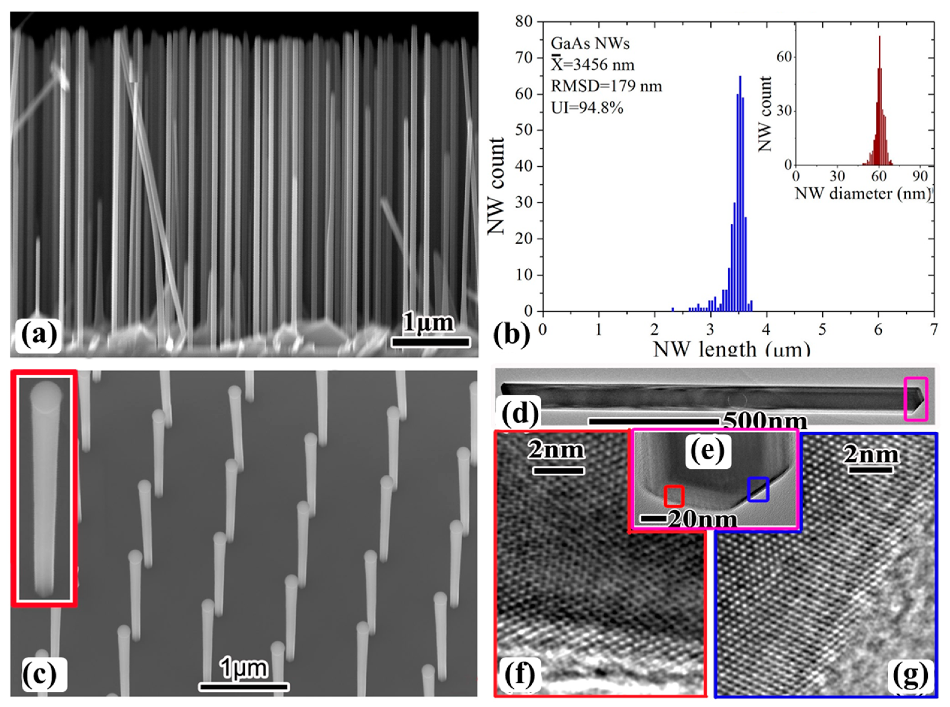
2. Integrating High-Quality III–Vs on Si

There are large lattice and thermal expansion coefficient mismatches between thin-film III–V materials and Si, causing large strain during the growth and leading to the generation of a high-density of defects, such as threading dislocations. NWs are filamentary crystals with a tailored diameter in the range from few nanometers to few hundred nanometers. NWs with a large surface-to-volume ratio and a small contact area between the NW and the Si substrate can elastically relieve the strain induced at the hetero-interface over a thickness of a few monolayers [30] Normally, no threading dislocations can be found at the upper part of the NWs. Thus, the lattice and thermal expansion mismatch issues between III–V epilayers and Si substrates can be effectively solved using the NW structure. Large-area high-quality III–V NW arrays can be grown on Si without wafer bowing and cracking, which promises an ideal marriage between the high-performance III–V NW optoelectronic devices and the mature low-cost large-scale Si microelectronic technologies.
To make large-area solar cells, the uniformity of NWs is critical. However, to reduce the cost, the growth on unpatterned Si substrates is preferred as no growth mask is needed, but it needs to use the droplet-catalyzed growth mode (except nitride) [31]. Uniformity control can be achieved through a nanoscale catalytic droplet, but suffers from the strong influence caused by the Gibbs−Thomson (GT) effect [32]. The GT effect makes the larger catalytic droplets have higher effective supersaturations and hence faster nucleation rates. Therefore, thicker NWs are commonly longer in length. Moreover, for NWs made of ternary or multinary materials, their composition uniformity can also be influenced by the droplet uniformity through the GT effect, making thinner NWs richer in elements with stronger chemical bonds. For example, the thinner GaAsP NWs are richer in P. To achieve good uniformity, good size uniformity of the catalytic droplets is necessary. As can be seen in Figure 1a,b, the uniform droplets can produce NWs with uniformity as high as >90%.
The III−V NW growth on unpatterned substrates typically follows a self-assembly mechanism where the NWs are randomly positioned. To realize better control of NW optical properties for achieving high-efficiency NW solar cells, each NW should be precisely located [33,34,35]. NW position control can be achieved using patterned substrates. Moreover, the growth on patterned substrates can suppress the parasitic bulk (cluster) deposition that often accompanies NW growth on unpatterned substrates, which is beneficial for making tandem solar cells. However, the growth on patterned Si substrates is more complex compared to that on unpatterned Si substrates and patterned III–V substrates, because the fast oxidization feature of Si makes the patterned holes covered/blocked by a thin layer of native oxide. The chemical etching via HF solution is not sufficient to obtain oxide-free holes for the NW growth. Zhang et al. developed an in situ, high-temperature (∼900 °C) cleaning technology that can thoroughly clean the patterned holes [36]. This cleaned substrate can be directly used for selective-area NW growth, but not directly for droplet-catalyzed NW growth. Zhang et al. showed that a Ga pre-deposition step is essential for the catalytic droplet formation in the oxide-free holes and further ensure the NW growth via vapor-liquid-solid (VLS) mode. (Figure 1c) [36]. They also found that the size of the patterned holes should not be bigger than the droplet size, otherwise it will affect the NW morphology by inducing parasitic growth at the bottom of the NWs.
The good crystal quality of NWs is the foundation of good solar cell performance. However, NWs tend to generate a high density of stacking faults that are a mixture of zinc-blende (ZB) and wurtzite (WZ) crystal structures. For the self-catalyzed mode, the droplet consumption can also generate a large number of defects. These defects can extend into the NW shell and degrade the shell crystal quality [37]. They can also regionally change the surface properties of NWs by producing new facets with different surface energies. Therefore, the nucleation features around these defective regions can be significantly modified, affecting the shell uniformity. This has been proofed by the Be-doped GaAsP shell with lumps along the length [37]. To grow high-quality shells, it is essential to eliminate the defects in the core NWs. Zhang et al. showed that the formation of Be−Ga alloy droplets can effectively suppress the WZ nucleation during GaAsP NW growth and droplet consumption, leading to the phase-pure ZB core NWs. On the high-quality core NWs, they achieved the growth of pure-ZB shells with highly regular morphology (Figure 1d–g) that demonstrated a one-order magnitude enhancement in room-temperature emission compared to the defective shells [37].
Therefore, position uncontrolled and controlled NWs with good uniformity, morphology, and crystal quality can be grown on Si substrates, which sets a strong foundation to build high-performance III–V solar cells on Si.

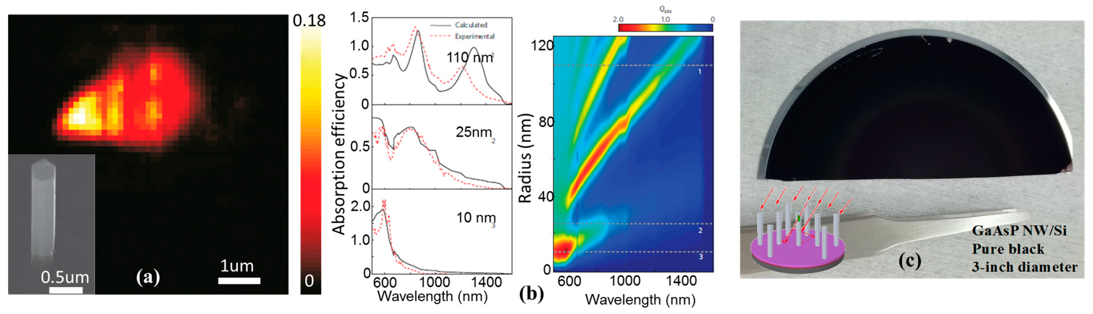
3. Superior Solar Photon Harvesting

In the thin-film solar cell structure, the light reflection from the front surface is one of the major energy loss mechanisms. For example, without any treatment, around 30% of the light illuminated at Si surface can be lost due to the reflection at the interface between air and Si [38]. To reduce this loss, conventional cells commonly need dielectric antireflection coatings, however, it is difficult to cover the entire absorption wavelength range. Broadband antireflection strategies can be achieved by light trapping schemes, such as inverted pyramid structures, however these add to the cost due to their complex fabrication process [39,40,41]. In contrast, NW arrays have strong antireflection ability with superior wavelength-, polarization-, and angle-dependent properties compared to planar structures, because NWs can form graded-refractive index layers [42]. Therefore, they can greatly reduce the light reflectance at the interface of two media by avoiding abrupt change in refractive index [43,44,45]. Diedenhofen et al. grew layers of GaP NWs on AlInP/GaAs substrates [46]. They found that NWs can greatly reduce the reflection and increase the light transmission into the substrate over broad spectral and angular ranges due to the graded refractive index. Zhu et al. fabricated a-Si:H NWs and realized greatly enhanced absorption over a large range of wavelengths and angles of incidence due to suppressed reflection [47]. More than 70% of the light was absorbed at angles of incidence up to 60°, which was significantly better than thin films (45%). In addition, the absorption of NW arrays was 70% at the band gap edge of a-Si:H, which was much higher than thin films (53%). Garnett et al. studied the transmission of the Si with and without Si NWs [48]. They found that the transmission over the entire spectral range (600 to 1100 nm) was reduced by factors of 2.9–7.8 for NWs with a length of 2 μm. Moreover, the transmission can be reduced more when the NWs are longer. When they increased the NW length to 5 μm, the transmission could be reduced by factors of 12–29. Tsakalakos et al. studied the reflectance of Si samples with and without Si NWs. They found that the reflectance of the NW film was less than 5% over the majority of the spectrum (below 700 nm), while that of the Si film was well above 30% [49].
NWs can have a greatly enhanced light-scattering effect due to subwavelength dimensions [50]. Strudley et al. studied the light transport inside a NW mat [51]. They found that mats of disordered high-refractive-index semiconductor NWs are one of the strongest three-dimensional scattering materials for light, which makes traditional light diffusion models no longer valid when describing photon transport and emission in strongly scattering NW mats. Their statistical analysis of intensity fluctuations showed that the transport for focused illumination is governed by a minimum of around three open transmission modes, which was a record low value for light in a three-dimensional medium. These effects are so strong that they observed a change in the distribution from Gaussian towards a skewed distribution that is only predicted in theory, but was not previously seen in a three-dimensional optical medium. Garnett et al. also observed similar phenomena [48]. They demonstrated that the path length of incident solar radiation in ordered arrays of Si NWs was 73 times longer. This extraordinary enhancement factor of light-trapping path length is above the randomized scattering (Lambertian) limit (2n2 ∼ 25 without a back reflector) and is superior to other light-trapping methods.
Semiconductor NWs have a unique nanoscale 1-dimensional structure which is typically on the order of the light wavelength. In addition, with the high refractive index, they behave as optical antennae [52] that can modify the absorption and emission properties [53]. When NWs are vertically standing, the absorption properties are determined by the waveguide modes [29,54]. NWs are more efficient in light absorption compared to planar materials of an equivalent volume. Krogstrup et al. observed that single NW solar cells with the vertical configuration have a remarkable increase in the absorption cross-section compared to their physical size (Figure 2a) [55]. At 1 sun illumination, a short-circuit current of 180 mA/cm2 was obtained from their vertically-standing GaAs NWs, which is more than one order of magnitude higher than that predicted from the Lambert–Beer law. This light-concentrating property gave their solar cells a high experimental efficiency of 40% that is above the Shockley–Queisser limit.
When the NW is lying horizontally, the absorption properties are determined by leaky-mode resonances or the Mie resonances supported by the NW (Figure 2b) [56], which provides an opportunity to engineer the light absorption in NWs by controlling their physical dimensions [57,58]. When the resonant modes supported by the NWs are leaky, the overlap between the incident electromagnetic field and the guided mode profile is maximized, facilitating efficient coupling with incident light. Sandhu et al. showed that an optimized single NW cell has a much higher open-circuit voltage compared to that of a bulk cell [59]. In addition, it also has a much higher short-circuit current when compared with the contributions of a region of semiconductor with the same volume located in the top surface of a bulk cell. Cao et al. observed that Leaky mode resonances can led to 250% increase in the light absorption per unit volume of material compared with the bulk [60].
All these advantages allow NW arrays to have advanced light trapping ability and hence strongly enhanced optical absorption in comparison with the thin-film devices [38,46,50]. This can significantly enhance the broadband light absorption over a wide range of incident angles, especially the near and below band gap absorption [61]. Wen et al. analyzed the efficient light trapping for GaAs NW arrays and found that the NW arrays have superior absorption characteristic (>90%) over thin-film (~60%) and can absorb 500% more photons per unit volume material, due to the combined effects of intrinsic antireflection and efficient excitation of resonant modes [62]. The study also revealed that an optimized geometry design can absorb 90% of above-bandgap sunlight despite the low volume filling ratio. Zhang et al. studied the light trapping properties of InGaAs NWs and found the short-circuit current can reach 61.3 mA/cm2, which is three times higher than that of thin-film layers with the same thickness [63]. Lin et al. simulated the absorption enhancement in terms of ultimate efficiency of Si NW devices, and suggested that an optimized SiNW array with a lattice constant of 600 nm and a wire diameter of 540 nm can have an ultimate efficiency that is 72.4% higher than a Si thin-film device of equal thickness [35]. Kelzenberg et al. demonstrated experimentally that Si NW arrays with a very small filling fraction (∼5%) can achieve up to 96% peak absorption, and can absorb up to 85% of above-bandgap direct sunlight each day [34]. This enhanced near-infrared absorption allows their overall sunlight absorption to exceed the ray-optics light-trapping absorption limit over a broad range of incidence angles for an equivalent volume of randomly textured planar Si. Guo et al. studied the influence of GaAs NW diameter D, length L, and filling ratio D/P on the absorption [64]. The optimal results for the normal light incidence were evaluated as D = 180 nm, L = 2 μm, and D/P = 0.5, which can lead to an absorption that exceeds 90% in the visible light region. This is much higher than that of thin films with the same thickness, due to the combined effects of the intrinsic antireflection and efficient excitation of resonant modes. For the oblique incidence, their modelling showed that perfect antireflection (>80%) can be achieved at incident angles up to 60°. Anttu et al. compared the efficiency of InP NW array solar cells with that of the conventional InP bulk solar cells [65]. They considered a NW array of 400 nm period, 4 μm length, and 170 nm diameter, which can produce 96% of the short-circuit current obtainable in the perfectly absorbing InP bulk cell. Besides, the NW solar cell emits fewer photons (especially into the substrate) than the bulk cell at thermal equilibrium, which allows for a higher open circuit-voltage. As a result, NWs longer than 4 μm can actually show, despite producing a lower short-circuit current, an efficiency limit of up to 32.5% that is higher than the bulk cells (31.0%). Callahan et al. also suggested with modelling that NW solar cells can exceed the ray optic light trapping limit [61]. This is supported by Wallentin et al [20]. They used ~1.5 μm-long 180-nm-diameter InP NWs to make solar cells. The NWs surface coverage was only 12% and the amount of InP material was only 1/10,000th of planar cells. Due to the resonant light trapping in NWs, the share of sunlight converted into photocurrent (71%) was six times the limit in a simple ray optics description. As a result, they can generate a short-circuit current which was about 83% of the best InP planar cells, and efficiencies up to 13.8% (comparable to the record planar InP cell) were achieved. Anttu et al. also found that 94% of the incident solar light can be absorbed by cylindrical NWs with a length of 2 µm, pitch of 400 nm, and a diameter of 241 nm [66]. Similar work has been done by other researchers [35,42,46,50,67,68,69,70,71,72,73,74,75,76,77,78,79,80].
Besides, the NW can also guide the below-band-gap photons into the substrate. Diedenhofen et al. found that more than 90% of the photons with energy lower than the InP absorption, were coupled into the underlying substrate by the InP NWs, which is highly favorable for multijunction devices [81].
Therefore, NWs have superior solar photon harvesting functions which are highly suitable for making photovoltaics. This can also be supported by the pure-black color of the 1.7 eV GaAsP NWs/Si sample shown in Figure 2c. Due to the advanced light absorption, the NW device can use a much smaller quantity of deposited material to achieve higher absorption efficiency compared with its thin-film counterparts. This can greatly reduce the cost, which has until now been prohibitive for thin-film III–V solar cells, so that NW-based solar cells are cost competitive with Si solar cells [20].

4. Superior Extraction Scheme for Photon-Generated Carriers

One of the key requirements for solar cells to achieve a high efficiency is the ability to maintain a large optical thickness to facilitate efficient light absorption and a small electrical thickness to facilitate efficient photo-generated carrier collection at the contacts. The collection efficiency of photon-generated carriers depends strongly on the minority carrier diffusion length, which decreases rapidly with the increase of defect density [82]. The generated carriers will be wasted if they are more than one diffusion length away from the space charge region. In a traditional thin-film device, the collection path of the generated carriers is parallel to the solar photon travelling path (Figure 3, left) [83]. Therefore, the requirement for a thick enough absorption material puts high demand on the crystal quality, so that the carriers can pass through without substantial recombination. The shape anisotropy of NWs provides opportunities to decouple the optical and electrical thickness of solar cells using the co-axial p–n junction structure (Figure 3, right) [18,82]. It absorbs the light along the whole NW, while the generated carriers can be efficiently separated in the radial direction. The radial distance that carriers need to travel (in hundreds nm range) is normally much smaller than, or comparable with, the minority carrier diffusion length. Therefore, the orthogonally decoupled light absorption and carrier separation paths can lead to low bulk recombination, and hence high efficiency. In addition, the NWs have a large surface-to-volume ratio, which offers a large junction area (up to 103 times larger than thin films) that can further enhance the charge separation efficiency. The study showed that the influence of changing the diffusion length under radial junction is less than in planar junction [84]. Kayes et al. studied the influence of carrier diffusion length on the Si device efficiency with a radial p–n junction geometry [82]. When they assumed very low diffusion length (100 nm), the maximum efficiency of the p–n junction device and the planar geometry were 11% and 1.5%, respectively. For a cell with carrier diffusion length 1 μm, the maximum efficiency of the radial p–n junction geometry and the planar geometry were 13%, and 5%, respectively. Pei et al. performed numerical simulations on amorphous-silicon (a-Si) NW solar cells and found that the co-axial p–n junction structure can overcome the efficiency limit of an a-Si solar cell [85]. They showed that the photocurrent of the a-Si solar cell with a 4000-nm-long NW was nearly 40% more than that of a planar a-Si solar cell. A conversion efficiency of 11.6% was obtained, which was enhanced by around 32%.
For III–V materials with a long carrier diffusion length, the difference of the performance between the planar and radial structures was not as obvious as that for Si. However, NWs have a large surface-to-volume ratio and hence a high-density of surface states. A study from Christesen et al. revealed that the NW devices with radial p–i–n structures are “surprisingly insensitive to surface recombination” compared to the ones with axial structures [86,87]. The internal quantum efficiencies of radial devices can be as high as 95% even with high surface recombination velocities (SRVs) of 105 cm/s, while axial devices require substantially lower values of 103−104 cm/s to produce the same level of performance because their depletion region is exposed to the surface. Apart from quantum efficiency, the open-circuit voltages of radial devices can be nearly twice that of axial devices.
All those advantages enable us to use lower-purity, less-expensive materials with low minority carrier diffusion lengths to build high-efficiency solar cells. As a result, the use of NW structure can significantly reduce the device cost. These merits of NWs make the development of high-efficiency and low-cost solar cells promising, and hence have the potential to revolutionize solar energy harvesting technology.

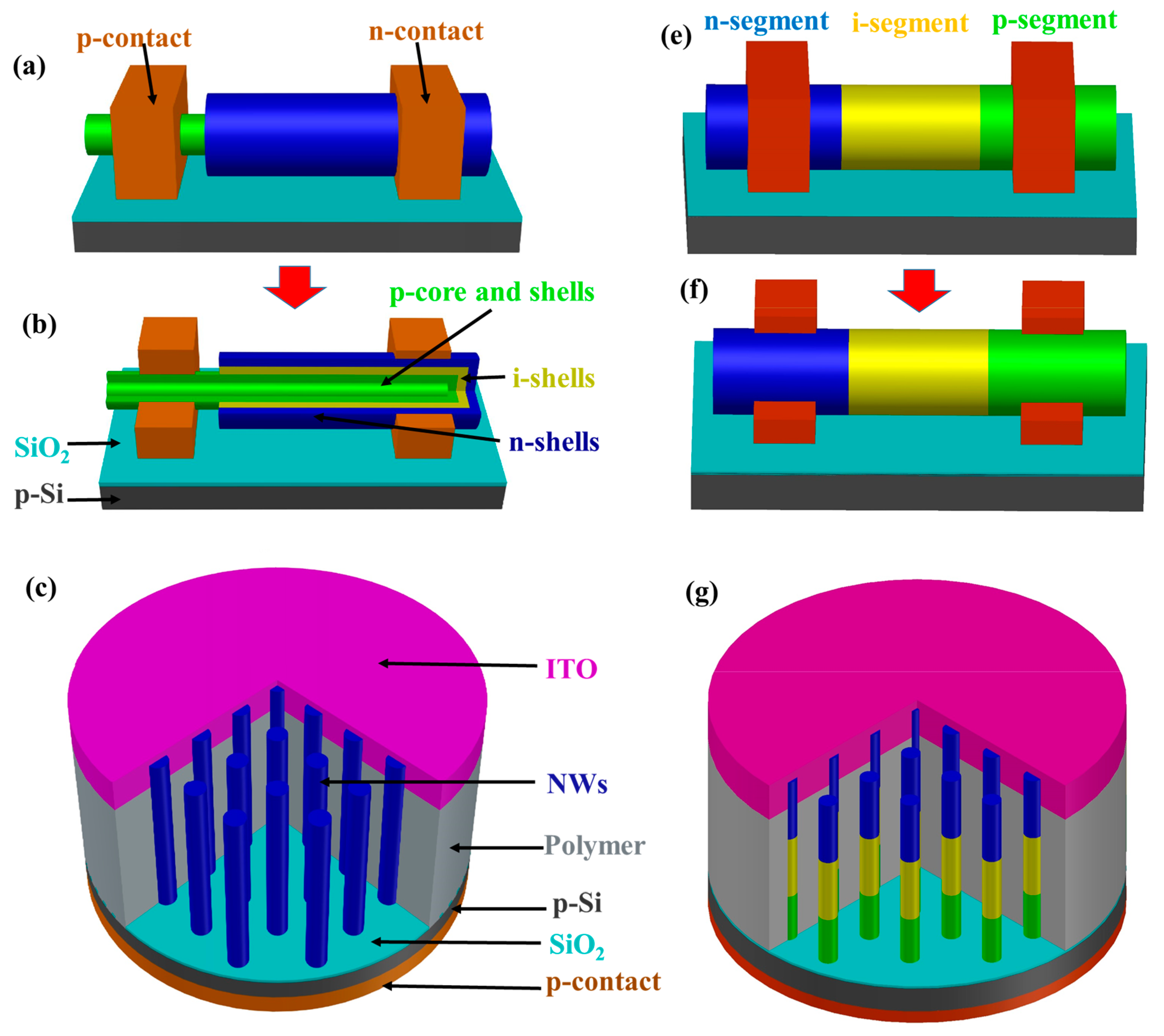
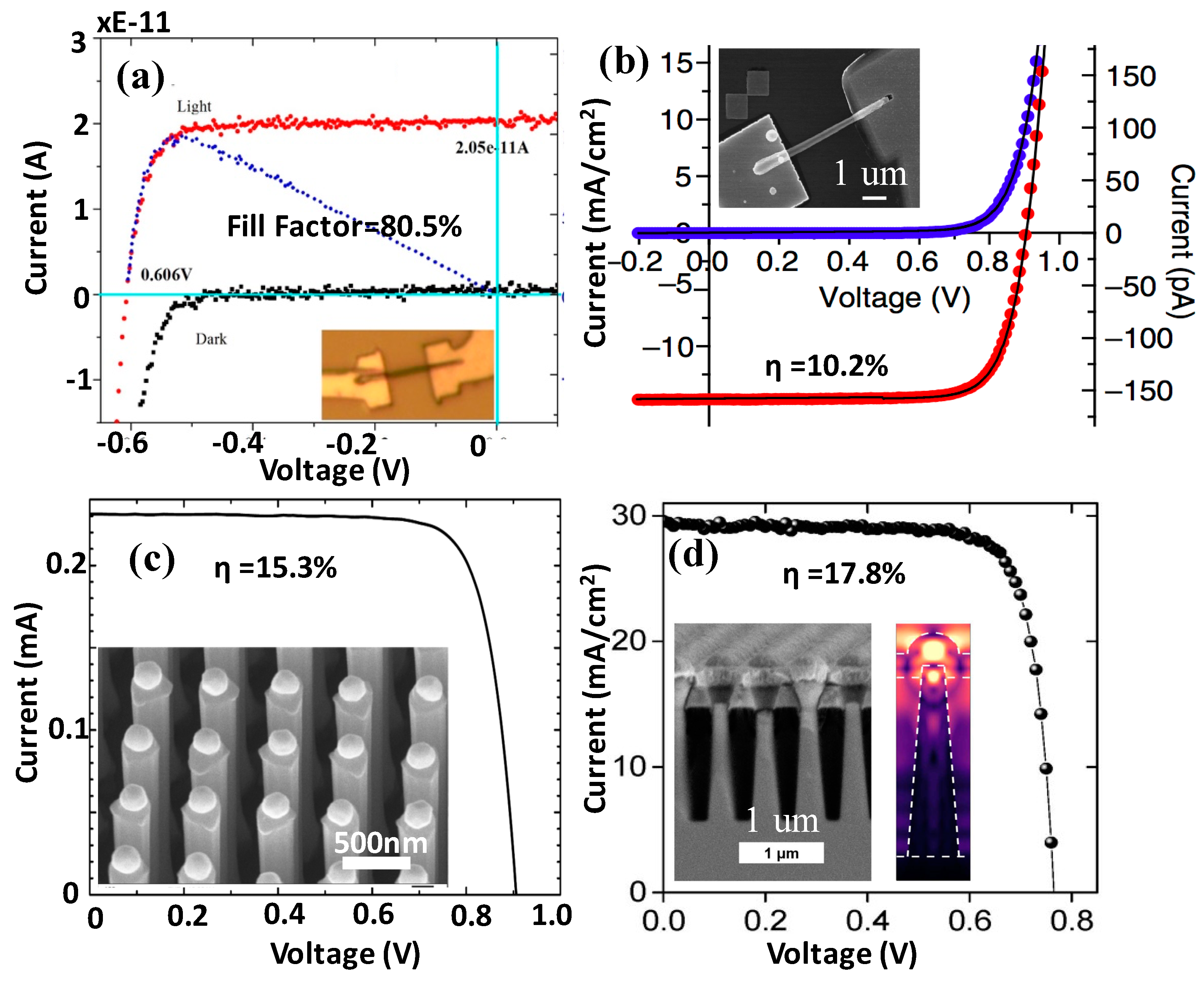
5. Single-Junction Solar Cells

To make NW solar cells, the first step is to achieve good Ohmic contact. However, the high-density surface states of NWs make it challenging because they can pin the Fermi level at the NW surface to the middle of the band gap [88,89]. When NWs contact metal, the pinning can produce a Schottky barrier and seriously hinder the formation of Ohmic contact. It has been reported that unpassivated GaAs NWs will be seriously depleted when the diameter is below 100 nm, making Ohmic contact formation even more difficult, especially for NWs with a smaller size [90]. Zhang et al. optimized the NW doping and the annealing condition of AuZn contact and achieved good Ohmic contact on GaAs NWs with a diameter as small as 50~60 nm [91]. This is the smallest III–V NWs diameter reported so far with Ohmic contacts, which gives valuable information on how small the NWs can be, while still allowing good Ohmic contact.
Divided by size, there are single (Figure 4a,b,e,f) and large-area (Figure 4c,g) NW devices [20,92,93,94,95,96,97,98]. The large-area photovoltaics can generate a large volume of power or strong signal. However, the fabrication of large-area devices is frequently hold back by the challenges in pinpointing the bottle necks due to too many performance-affecting factors, such as the contact quality, p–i–n junction quality, and doping profile. The intrinsic limiting factors caused by the NW itself can be identified by studying single NW devices, providing valuable information for the development of large-area devices. Moreover, single NW photovoltaics can also be used in high-density integrated circuits (ICs). For example, they can function as photon detectors in Si-based photonics, greatly facilitating the chip-to-chip and system-to-system optical communications [99]. Further divided by structure, there are radial (Figure 4a–c) [98] and axial junction (Figure 4e–g) [92] solar cells. The fabrication of single NW devices with radial p–i–n junctions is more difficult. Shell removal is one of the major challenges, making most of the devices limited in performance [100,101]. For instance, the widely-used self-catalyzed NWs commonly have a p-type doped core that is covered by i- and n-shells, forming a p–i–n junction. To make p-type contact, the n- and i-shells must be removed so that p-contact metal can be deposited onto the exposed p-regions (Figure 4a,b). Due to the small size, it is difficult to perform the shell removal uniformly and precisely. Besides, it commonly uses wet etching to perform the shell removal [102]. When the NWs have stacking faults, it can be even more challenging to achieve uniform shell removal, because the stacking faults can give rise to new surface facets with higher surface energies and hence these regions can be corroded faster. Zhang et al. used focused ion beam (FIB) to mill away the surface n- and i-layers and achieved a uniform p-core [91]. After putting on the p- and n-contacts, the single GaAs NW solar cell showed a world-record-high fill factor of 80.5% and a stable photo response (Figure 5a). In contrast, the fabrication of single NW solar cells with an axial junction is much easier because no shell removal is needed (Figure 4e,f). The structure for large-area NW solar cells are quite similar despite different junction configurations. As illustrated in Figure 4c,g, the contacts are commonly in a top-bottom configuration, with one contact at back of the substrate and the other one at the tip of NWs. The quality of the top contact has more significant influence on the solar cell performance. Fang et al. found that the major factor that limited the performance of their large-area solar cell was the low carrier-collection efficiency of the top contact [103]. Besides, it needs to be noted that devices with radial junctions have more limitations of fabrication technique because the junction layers are very thin and can easily be damaged by unoptimized fabrication processes, such as annealing.
There has been extensive study of the fabrication of single NW devices, such as solar cells and detectors [104,105,106]. However, most of them are with axial p–i–n structures because it is comparatively easy to fabricate contacts [107,108]. However, so far, the highest efficiency of single horizontal NW solar cell is 10.2% reported by Holm et al. using GaAsP NWs with radial p–i–n junctions (Figure 5b) [109]. Vertically standing NWs are higher in efficiency due to their light-concentrating property. Ko et al. achieved an efficiency of 19.6% using InP NWs [110]. Krogstrup et al. even reported a high experimental efficiency of 40% using GaAs NWs [55].
Large-area solar cells are rapidly developing [111]. Wallentin et al. reported an InP NW array solar cell with an efficiency of 13.8%, which is the first large-area solar cell with an efficiency higher than 10% [20]. Afterwards, Cui et al. achieved an efficiency of 11.1% with InP NW arrays [93]. Then, Åberg et al. achieved 15.3% using GaAs NW arrays (Figure 5c) [92]. So far, the world record is held by Hwang et al. with an efficiency of 18.9% using very thick NWs (microwires), followed by van Dam et al. with an efficiency of 17.8% (Figure 5d) [112,113]. Although the NWs used in these two reports were via top-down etching, the achievement still shows the promising future of making NW solar cells. All these four outstanding works are based on III–V substrates. To reduce the cost, developing Si-based solar cells is critical. However, most of them are low in efficiency [114,115,116,117,118,119]. It also needs to be mentioned that the solar cells with good efficiencies are achieved with axial p–i–n junctions. The efficiency of those with radial p–i–n junctions is still lower than 7.5% [95,96,114,120,121,122,123,124,125,126]. This could be because it is relatively difficult to fabricate the contact on a radial junction. Each layer in the radial junction is very thin and easily damaged, putting higher demand on the fabrication technology.
So far, the efficiency of single NW solar cells and large-area bottom-up solar cells still needs to be improved. The breakthrough of the fabrication techniques for both single and large-area NW solar cells makes the development of high-efficiency NW solar cells promising.

6. Design for Novel High-Efficiency and Low-Cost Solar Cells

The unique structure and advanced properties of NWs give more freedom in constructing novel solar cells with high efficiency and low cost.
Tandem solar cells on Si: In the traditional thin-film structure, multijunction cells allow for high efficiency, but need to use the expensive Ge substrates. The integration of III–V solar cells on Si can greatly reduce the cost, which is extremely challenging. The ability to grow III–V NWs on Si substrates has thus attracted great attention in the design of two-junction solar cells consisting of a bottom Si cell and a top III–V NW cell [18,127,128,129,130,131]. The optimum structure requires the top NW cell to have a direct bandgap of near 1.7 eV, which can be achieved using a number of compound semiconductor material systems, such as GaAs0.77P0.23, Al0.19Ga0.81As, In0.65Ga0.35P, Al0.13In0.87P, and Al0.57In0.43As. The optimum structure also requires equal current from each subcell, namely a current-matching condition [132,133]. This can be realized by adjusting the diameter, length, and period of the NW array. Therefore, NW solar cells have many more degrees of freedom compared with thin-film solar cells, whose current-matching is achieved by adjusting the thickness of the absorbing layer in each subcell. Hu et al. showed how to design the current matching between 1.7 eV III–V NW top cell and 1.1 eV Si planar bottom cell by tuning the NW diameter and period [134]. The highest photocurrent density of 17.8 mA cm−2 can be obtained with a diameter of 180 nm, period of 350 nm, and length of 5 μm. This corresponds to 89.4% absorption of the AM1.5G spectrum. It is commonly accepted that a promising efficiency above 30% under one sun illumination could be obtained at the current matching geometries [135]. Some researchers even suggest that it can go above 34% [127,136]. Early in 2014, Holm et al. reported the III–V NW/Si solar cells by using 1.7eV GaAsP NWs [126]. However, due to the unoptimized quality and structure, the efficiency was only 4%. Later on, Yao et al. made important progress and paid special attention to the current-matching between top and bottom cells [97]. They made GaAs NW/Si tandem cells and achieved an open circuit voltage of 0.956 V and an efficiency of 11.4% (Figure 6a).
Axial tandem solar cells: NWs have a small cross section, which allows NWs to accommodate big strains axially and laterally. This can greatly facilitate the integration of materials with large lattice mismatch, providing more freedom in the structure design compared with thin-film devices [137]. The axial junction can distribute the strain across the interface, which can further relax the strain gradually and elastically. Therefore, for an axial NW heterojunction structure with lattice mismatch, there will be a critical diameter below which no interface dislocation can be introduced regardless of the length [138,139]. Dislocation-free heterojunctions have been realized even with a large lattice mismatch, such as GaAs/GaP, InAs/InSb, and InAs/InP [137,140,141]. Similarly, the NW core can share part of the mismatch strain and therefore drastically reduce the strain in the shell [142,143,144,145,146,147]. NW core–shell structure can thus accommodate larger lattice mismatch compared with thin-film structures [148,149]. For example, Nazarenko et al. demonstrated that a 160-nm defect-free GaAs shell can be grown on In0.2Ga0.8As core NWs despite a large lattice mismatch of 2%, which is much thicker than the allowed thickness in thin-films (10 nm) [150]. With this advantage, Chen et al. proposed an axial Ga0.51In0.49P/InP dual-junction solar cell with axial p–i–n junctions and a maximum efficiency of 38.5% could be achieved [151]. Wang et al. proposed a novel NW solar cells with several radial p–n junctions connected axially. Therefore, the solar spectrum can be separated and absorbed in the top and bottom cells with respect to the wavelength (Figure 6b) [152]. The unique structure of NW p–n junctions enables substantial light absorption along the NW length and efficient carrier separation and collection in the radial direction. The simulation results revealed a high conversion efficiency of 16.8% at a low filling ratio of 0.196, which is much higher than the axial tandem p–n junctions under the same conditions (8.87%). After matching the current, a promising efficiency of 19.9% can be achieved at a low filling ratio of 0.283. Heurlin et al, demonstrated the possibility of building tunnel junctions inside a single NW [108]. They connected two p–n junctions axially in a single InP NW by a heavily doped p–n tunnel junction, forming a tandem NW SC. An open-circuit voltage of 1.15 V was achieved under ~1 sun illumination, which was an increase of 67% compared to the single p–n junction device. Hocevar et al. reported the growth of hybrid axial GaP/Si heterojunctions [153]. This integration of different materials in the SiNWs opens new approaches to achieving high-efficiency NW solar cells, such as novel 1.7 eV III–V/Si NW solar cells.
Multiterminal NW solar cell: Dorodnyy et al. proposed a multiterminal NW solar cell design (Figure 6c) [154]. The design uses NWs of different band gaps. For example, the authors used Al0.54Ga0.46As, GaAs, and In0.37Ga0.63As NWs, which can form an ideal band gap combination (2.01, 1.42, and 0.93 eV, correspondingly). These three types of NWs are mixed evenly on the sample. Therefore, they can split the incoming solar spectrum spatially and NWs with different band gaps separately convert it into electrical power. Besides, these three types of NWs have separated contacts, which can circumvent the current matching requirement in common tandem solar cells with the one-pair-contact structure, giving more freedom in device design. Therefore, a theoretical conversion efficiency of 48.3% can be achieved. This multiterminal contacting device can be fabricated with the technology close to that used in a standard CMOS fabrication line. However, the major challenge would be the difficulty of growing different NW groups with different lengths required for device fabrication.
Inorganic NW/organic hybrid solar cells: Compared with organic polymers, inorganic materials commonly have a high carrier mobility and affinity. In contrast, organic polymers commonly have a low carrier mobility and short lifetime, which leads to a low device efficiency. However, they are low in production cost. Therefore, researchers are trying to combine together the advantages of the two material systems, which has been demonstrated extensively in the planar solar cells [155,156]. When inorganic materials are made into the NW structure, the devices can have a very large surface-to-volume ratio, which can provide a large surface area. A greatly enhanced efficiency is hence expected for the inorganic NW/polymer combination due to the fast and efficient charge separation/collection [157]. Bi et al. showed the effectiveness of using the NW structure in making inorganic NW/polymers [158]. They introduced GaAs NWs into the 3-hexylthiophene (P3HT)/GaAs hybrid solar cells and reached an efficiency of 1.04% (2.6 sun), while the reference planar GaAs had negligible photovoltaic response. Chao et al. reported a similar phenomenon in making poly(3,4-ethylenedio xythiophene):poly(styrenesulfonate) (PEDOT:PSS) solar cells [159]. They found that compared to the planar GaAs/PEDOT:PSS cells, the efficiency of GaAs NW/PEDOT:PSS under AM 1.5 global one sun illumination was improved from 0.29% to 5.8%. Shen et al. compared the inorganic–organic hybrid Si solar cells with and without Si NWs in between [160]. They found the presence of Si NW can increase the efficiency from 3.6~6% to 7.5~8.4% due to the excellent output characteristics of light harvesting capability and charge extraction efficiency. For this type of hybrid solar cells, the organic layers should not be thicker than the exciton diffusion length. Tsai et al. built Si NW arrays/P3HT hybrid solar cells [161]. They found that the core–shell hybrid solar cells with suitable polymer thickness exhibited a 61% improvement in the short-circuit current and a 31.1% enhancement in the conversion efficiency as compared to the P3HT-infiltrated Si NW solar cells with very thick polymer layers that formed a flat air–polymer cell interface. Besides, the interface carrier recombination can seriously hinder the performance of hybrid organic/inorganic hetero-junction solar cells. Wang et al. studied the influence of surface treatment on the performance of Si NW/PEDOT:PSS hybrid solar cells [162]. They generated a surface sacrificial oxide on the Si NWs, and then followed with a HF etching process to remove the oxide, which can achieve a clean Si NW surface without contaminates, such as Au. This increased the efficiency from about 10% to 12.4%. Yu et al. introduced an intermediate 1,1-bis[(di-4-tolylamino)phenyl]cyclohexane (TAPC) layer into Si NW/PEDOT:PSS hybrid heterojunction solar cells. This can effectively block the strong oxidation reaction occurring between PEDOT:PSS and Si, which improved the device characteristics and assurances for reliability [163]. This insertion layer can also increase the minority carrier lifetime because of an energy offset at the heterojunction interface. As a result of the interface modification, the hybrid heterojunction cell demonstrated a high efficiency of 13.01% that was superior to the reference counterpart (12.01%). This insertion layer also enhanced the Voc from 0.52 to 0.54 V, and an FF from 66.4 to 69.5%. Um et al. fabricated Si NW/PEDOT:PSS solar cells [164]. In their design, a Ag/SiO2 electrode was embedded into the Si substrate and positioned between Si NW arrays underneath PEDOT:PSS, which can facilitate suppressing recombinations at the Si–Ag interface and notably improve the fabrication reproducibility. With this design, their cell exhibited a power conversion efficiency of up to 16.1% with an open-circuit voltage of 607 mV and a short circuit current density of 34 mA/cm2. Wei et al. built a hierarchical hybrid solar cell (Figure 6d) [165]. They made n-Si NWs on n-Si micro-pyramid arrays, and then coated the NWs with PEDOT:PSS. This design can greatly enhance the light antireflection ability of the surface by combining the advantages from both nano- and microstructures. This solar cell had an efficiency of 11.48%, which was higher than the planar solar cells (6.16~7.59%) and the micropyramid solar cells without NWs (10.37~10.96%). At present, the polymer/NW hybrid solar cell has reached an efficiency of well over 10% [164,166]. However, these high-efficiency hybrid solar cells were using top-down etched NWs [167,168]. For bottom-up NW solar cells, the efficiency is commonly lower than 5% [169], which could be due to the challenges of managing the interface properties between the NW and the substrate.
Branched solar cells: Lundgren et al. proposed a high-absorption structure using a novel branched NW (BNW) configuration (Figure 6e), which can be used in the fabrication of solar cells [170]. BNW arrays have the potential to greatly increase the optical absorption compared with normal NW array structures. They modeled the properties of branched Si NWs and achieved a maximum absorption of over 95% at 500 nm wavelength. Besides, they also achieved at least a factor of 4 improvement in absorbing the photons in the difficult low energy region (~1 μm). There has been great progress in fabricating branched NWs [171]. For example, Wang et al. have demonstrated the growth of Si and GaN NWs with multigeneration branches [172]. Baxter et al. used branched ZnO NWs to construct dye-sensitized solar cells and achieved an internal quantum efficiencies of 70%, which benefited from the improved electron transport [173].
NW solar cells on cheap substrates: Unlike thin-film structures, NW growth has much wider choices in the substrate selection, which benefits from its good strain accommodation ability mentioned above. The integration between large lattice mis-matched material systems have been reported, such as InP/Si (8.1%) and InAs/Si (11.6%) [174,175,176,177,178]. Besides the single crystalline and polycrystalline substrates, the NWs can also be grown on graphene, carbon nanotube, fibre-textured silicon thin film, amorphous Si, glass, and indium tin oxide [179,180,181,182,183,184]. O’Donnell et al. grew Si NW solar cells on glass substrates and achieved and efficiency of 5.6% [185]. Mohseni et al. presented a novel solar cells design employing InGaAs NW arrays grown directly by van der Waals epitaxy on graphene films [123]. An efficiency of 2.51% was demonstrated despite the unoptimized bandgap of NWs. This demonstration shows that the substrate limitation in traditional thin-film technology can be broken. Even on the non-crystal substrates, the III–V devices could still be integrated through the surface treatment by graphene. Therefore, NW solar cell can greatly reduce the cost due to the use of cheap substrates.
Flexible solar cells: For some special occasions, novel device properties will be needed. Lightweight and flexibility are two of the desired properties which can substantially reduce the facility weight, minimize the transportation cost, and lead to the realization of smart solar cells, such as integrating flexible cells into clothing [186]. NWs with 1-dimensional structure provide unique advantages in realizing these advanced functions, as they can be buried into polymers and then easily peeled off from the substrates [187]. Fan et al. demonstrated flexible CdS NW based CdTe solar cells with an efficiency of ~6% (Figure 6f) [188]. Kwon et al. made flexible solar cells using Si NWs and achieved an efficiency of >8% [189]. Han et al. fabricated flexible GaAs NW solar cells with NWs lying horizontally and achieved a high efficiency of 16% under air mass 1.5 global illumination [190].
These novel designs provide highly promising ways to greatly reduce the cost and boost the efficiency of solar cells, which may revolutionize present solar cell technology.

7. Challenges in Making NW Solar Cells

Despite the great advantages of using NWs in making solar cells, there are still some challenges that need significant effort.
Characterization: The nanoscale 1-dimensional structure makes it challenging to quantify the electrical properties of NWs using conventional measurement methods. Conventional electrical transport measurements (e.g. Hall Effect, van der Pauw, and field-effect transistor analysis), although appropriate for planar layers, are considerably more challenging to apply to NWs. The quasi one-dimensional NW geometry precludes conventional Hall Effect measurements unless highly specialized procedures are employed to make electrical contacts to the NWs [191,192]. Field-effect measurements are widely used on NWs, but their interpretation is heavily influenced by modelling assumptions and the uncertainty in the estimated gate capacitance term [193,194]. Crucially, these errors can also depend on the NW diameter, systematically distorting the apparent relationship between diameter and the determined mobilities [194]. Difficulties in obtaining ohmic contacts, particularly to p-type materials, [194] and the artefacts that arise due to metal contacts, can confound meaningful interpretation of contact-based measurements. Without these key electrical data, such as charge carrier lifetimes, mobilities, diffusion lengths, doping levels, and surface recombination velocities, it is extremely difficult to optimize NW growth and structure for rational, targeted device development.
Surface passivation: Due to the nanoscale 1–D cylindrical structure, NWs have a large surface-to-volume ratio and the surface area can be over 1000 times larger compared with thin-film structures. The surface of a crystal breaks the three-dimensional bulk periodicity and there is an associated change in the electronic structure [195]. The large surface area inherent to NWs exacerbates the effects of surface states. Surface states can trap carriers, which causes carrier depletion and band bending in the near surface region, affecting the metal contact fabrication [196,197] More seriously, surface states are also high-efficiency carrier loss centers that can lead to a low device efficiency [198]. The high surface recombination velocity results in the annihilation of minority carriers that would otherwise contribute to a portion of the output in the PV device. Consequently, bare NWs exhibit extremely short carrier lifetimes of only a few picoseconds [199]. It has been reported that core–shell GaAs NWs applied to solar cells have revealed conversion efficiencies ranging from 0.83% [200] for as-grown devices to 2.54% [96] for devices post-treated with ammonium sulphide agents. Similarly, InGaP passivation can increase the efficiency of GaAs NWs solar cells from 1.02% to 6.63% [95]. Nakai et al. also reported the increase of the efficiency of GaAs NW solar cells from 0.71% to 4% by introducing an InGaP surface passivation layer [201]. This phenomenon has also been found on different material systems. For example, Zhang et al. fabricated ZnO/CdTe core–shell NW solar cells and got negligible PCE. They inserted a thin CdS interlayer shell to provide more effective passivation to the ZnO surface and improved the PCE to 4% [202]. A similar discovery was also reported by Kartopu et al [203]. These reports show the influence of surface states and the importance of surface passivation. For Si NWs, the passivation is relatively mature, and the surface dandling bonds can be effectively reduced using amorphous silicon, carbon, SiN, SiO2, and Al2O3 [204,205,206,207]. However, the passivation for III–Vs is less developed compared with Si. Currently, the surface passivation is commonly using materials with higher band gap to block carriers away from surface, such as AlGaAs for GaAs NWs, or using materials with lower surface recombination rate, such as InP or InGaP. However, traditional surface-state characterization methods typically have a large deviation range and cannot give an accurate value of the key parameters, such as surface recombination rates [208]. As a result, it is challenging to quantitatively assess the passivation effect with high accuracy, which makes it difficult to predict how much further improvement is needed. That could be why most reported research is comparative study and only shows some improvement based on few parameters, rather than give a quantitative value of surface state passivation. Therefore, more advanced characterization methods will be required to systematically develop highly-efficient and robust surface-passivation techniques.
P–i–n junctions: The p–i–n junction is the most critical part for most of the solar cells. It consists of three regions. As the name suggests, there is an intrinsic/undoped layer sandwiched between a p- and an n-doped regions. The Fermi levels of the doped regions must be aligned at the same level. The potential difference across the -layer, called the built-in potential, is the main driving force to separate photon-generated electrons and holes to n and p regions for collection, respectively. The accumulated charge carriers can contribute to the current flow when connected to outer circuits. The quality of p–i–n junctions depends significantly on the doping, which has been widely studied in thin-film structures. However, NW growth mechanisms and environment are typically different from those of thin-film structures, with different growth temperatures, III–V ratios, and growth facets. This can significantly influence the doping incorporation pathways (through sidewalls or droplets), efficiency, doping type, and ionization energy, which gives special demands on NW doping to construct high-quality junctions [209,210,211]. For example, the ionization energy of dopants has been reported to increase with decreasing NW diameter, resulting in a carrier density lower than expected value [212]. Dopant incorporation may also be affected by the “self-purification effect” in the NW, that is, at nanodimensions, impurities with high formation energy will be expelled out of the nanocrystal to lower system Gibbs free energy [213,214]. The small dimensions and large surface-to-volume ratio of NWs can also affect the junction performance. The surface states can trap a large number of carriers, lowering the effective doping concentration [215]. The p-, i-, and n-layers are very thin (<100 nm) in the circular core–shell structure, which are quite susceptible to surface states. Moreover, the small size makes it more challenging to balance the effective dopant concentration and hence carrier density in the p and n regions. If the concentration of one type of effective dopant is significantly more than the other, it would be difficult to form p–i–n junction. Thus, the knowledge obtained from previous thin-film studies cannot transfer directly to NWs. There is a lack of systematic study on how to build high-quality p–i–n junctions based on this ultrathin and circular structure, because there is no effective way to characterize the junction quality. Although atom-probe measurement gives great insight into dopant incorporation, it unfortunately cannot provide insight into the density of ionized (and therefore active) dopants [216]. Therefore, more effort will be required to systematically study the optimization of p–i–n junctions. Fiordaliso et al. and Boulanger et al. demonstrated a useful technology to characterize the quality of NW p–i–n junctions [114,217]. By using off-axis electron holography, the electrostatic potentials across the p–n junction can be mapped out, providing direct information on the built-in potential. This can greatly facilitate the development of high-quality junction.
NW solar cell device fabrication: The solar cell fabrication technique for thin-film structures is well established. However, it cannot be used directly for the fabrication of NW solar cells, especially those with radial p–i–n junctions. The NW solar cell is a highly-compacted structure with radial p–i–n junctions of only a few hundreds of nanometers. The etching and annealing used in thin-film device fabrication can easily cause damage to the junction. Developing new fabrication technology for NW devices is time-consuming and costly. In particular, the lack of electrical data makes it difficult to identify if the failure is caused by the NW structure or the device fabrication process. So far, large-area solar cells with a high fill factor approaching 80% can be achieved [92,113], but on axial structures. The radial p–i–n structure has great advantages in making solar cells, but the device fabrication is still challenging, and the fill factor is commonly lower than 70% [122]. Very recently, a high fill factor of 80.5% from single NWs with radial p–i–n structure has been achieved by Zhang et al [91]. which is a big achievement in single NW device fabrication. Hopefully, this technology will promote the fabrication of large-area solar cells with radial p–i–n junctions. Moreover, the size of the solar cell is a critical factor that can decide its practical applications. Although there are already technologies that can produce high-quality NWs with wafer-scale uniformity, more study on scaling-up of NW solar cells is needed [218].

8. Conclusions

Compared with thin-film/planar/bulk materials, NWs can allow the integration of high-quality materials with good opto-electrical properties, such as III–Vs, onto cheap Si substrates, providing a highly-promising method to build high-efficiency, low-cost solar cells. NWs can greatly enhance the light absorption compared to planar material of an equivalent volume, which allows one to use a trace amount of expensive materials to achieve adequate light absorption. NWs can also provide superior extraction scheme for the photon-generated carriers, which can greatly enhance the external quantum efficiency. So far, single NW solar cells have achieved an efficiency of 10.2% for the horizontal structure and 40% for the vertical structure; the large-area structure has achieved an efficiency of 18.9%, which demonstrates the feasibility of building next-generation, high-efficiency, low-cost solar cells using the NW structure. All these promoted the design for novel higher-efficiency and lower-cost solar photovoltaics, such as NW/Si tandem solar cells, axial tandem NW solar cells, branched NW solar cells, inorganic NW/organic hybrid solar cells, NW solar cells on cheap substrates (graphene, carbon nanotube, fiber-textured silicon thin film, amorphous Si, glass, and indium tin oxide), and flexible solar cells. Despite the promising future and significant progress, there are some challenges in achieving high-efficiency NW solar cells. More effort is needed in developing more advanced technologies for characterization, surface passivation, p–i–n junctions, and NW solar cell device fabrication.

Funding

The authors acknowledge the support of Leverhulme Trust, EPSRC (grant nos. EP/P000916/1 and EP/P000886/1), and EPSRC National Epitaxy Facility.

Conflicts of Interest

The authors declare no conflict of interest.

References

  1. Husher, J.D. Beyond Global Warming: The Bigger Problem and Real Crisis; iUniverse, Inc.: Bloomington, IN, USA, 2007. [Google Scholar]
  2. Yu, K.; Chen, J. Enhancing solar cell efficiencies through 1-D nanostructures. Nanoscale Res. Lett. 2009, 4, 1. [Google Scholar] [CrossRef]
  3. Solar Cells Market Size—Industry Share Analysis Report 2024. Available online: https://www.gminsights.com/industry-analysis/solar-cells-market (accessed on 1 December 2016).
  4. Almansouri, I.; Ho-Baillie, A.; Bremner, S.P.; Green, M.A. Supercharging silicon solar cell performance by means of multijunction concept. IEEE J. Photovolt. 2015, 5, 968. [Google Scholar] [CrossRef]
  5. Essig, S.; Allebé, C.; Remo, T.; Geisz, J.F.; Steiner, M.A.; Horowitz, K.; Barraud, L.; Ward, J.S.; Schnabel, M.; Descoeudres, A.; et al. Raising the one-sun conversion efficiency of III–V/Si solar cells to 32.8% for two junctions and 35.9% for three junctions. Nat. Energy 2017, 2, 17144. [Google Scholar] [CrossRef]
  6. Abdul Hadi, S.; Fitzgerald, E.A.; Griffiths, S.; Nayfeh, A. III–V/Si dual junction solar cell at scale: Manufacturing cost estimates for step-cell based technology. J. Renew. Sustain. Energy 2018, 10, 015905. [Google Scholar] [CrossRef]
  7. Green, M.A.; Emery, K.; Hishikawa, Y.; Warta, W.; Dunlop, E.D. Solar cell efficiency tables (version 48). Prog. Photovolt. Res. Appl. 2016, 7, 905–913. [Google Scholar] [CrossRef]
  8. Marti, A.; Araújo, G.L. Limiting efficiencies for photovoltaic energy conversion in multigap systems. Sol. Energy Mater. Solar Cells 1996, 43, 203. [Google Scholar] [CrossRef]
  9. De Vos, A. Detailed balance limit of the efficiency of tandem solar cells. J. Phys. D Appl. Phys. 1980, 13, 839. [Google Scholar] [CrossRef]
  10. Abdul Hadi, S.; Fitzgerald, E.A.; Nayfeh, A. Theoretical efficiency limit for a two-terminal multijunction “step-cell” using detailed balance method. J. Appl. Phys. 2016, 119, 073104. [Google Scholar] [CrossRef]
  11. Kurtz, S.R.; Faine, P.; Olson, J.M. Modeling of two-junction, series-connected tandem solar cells using top-cell thickness as an adjustable parameter. J. Appl. Phys. 1990, 68, 1890. [Google Scholar] [CrossRef]
  12. Lieber, C.M.; Wang, Z.L. Functional nanowires. MRS Bull. 2007, 32, 99. [Google Scholar] [CrossRef]
  13. Zhang, Y.; Wu, J.; Aagesen, M.; Liu, H. III–V nanowires and nanowire optoelectronic devices. J. Phys. D Appl. Phys. 2015, 48, 463001. [Google Scholar] [CrossRef]
  14. Yan, R.; Gargas, D.; Yang, P. Nanowire photonics. Nat. Photonics 2009, 3, 569. [Google Scholar] [CrossRef]
  15. Dasgupta, N.P.; Sun, J.; Liu, C.; Brittman, S.; Andrews, S.C.; Lim, J.; Gao, H.; Yan, R.; Yang, P. 25th anniversary article: Semiconductor nanowires–synthesis, characterization, and applications. Adv. Mater. 2014, 26, 2137. [Google Scholar] [CrossRef] [PubMed]
  16. Yang, P.; Yan, R.; Fardy, M. Semiconductor nanowire: what’s next? Nano Lett. 2010, 10, 1529. [Google Scholar] [CrossRef] [PubMed]
  17. Reimer, M.E.; Bulgarini, G.; Akopian, N.; Hocevar, M.; Bavinck, M.B.; Verheijen, M.A.; Bakkers, E.P.A.M.; Kouwenhoven, L.P.; Zwiller, V. Bright single-photon sources in bottom-up tailored nanowires. Nat. Commun. 2012, 3, 737. [Google Scholar] [CrossRef] [PubMed]
  18. LaPierre, R.R. Numerical model of current-voltage characteristics and efficiency of GaAs nanowire solar cells. J. Appl. Phys. 2011, 109, 034311. [Google Scholar] [CrossRef]
  19. Cui, Y.; Van Dam, D.; Mann, S.A.; Van Hoof, N.J.J.; Van Veldhoven, P.J.; Garnett, E.C.; Haverkort, J.E.M. Boosting solar cell photovoltage via nanophotonic engineering. Nano Lett. 2016, 16, 6467–6471. [Google Scholar] [CrossRef] [PubMed]
  20. Wallentin, J.; Anttu, N.; Asoli, D.; Huffman, M.; Åberg, I.; Magnusson, M.H.; Siefer, G.; Fuss-Kailuweit, P.; Dimroth, F.; Witzigmann, B.; et al. InP nanowire array solar cells achieving 13.8% efficiency by exceeding the ray optics limit. Science 2013, 339, 1057. [Google Scholar] [CrossRef]
  21. Service, R.F. Performance of Nanowire Solar Cells on the Rise. Science 2013, 339, 263. [Google Scholar] [CrossRef]
  22. Yu, R.; Lin, Q.; Leung, S.F.; Fan, Z. Nanomaterials and nanostructures for efficient light absorption and photovoltaics. Nano Energy 2012, 1, 57–72. [Google Scholar] [CrossRef]
  23. Kapadia, R.; Fan, Z.; Takei, K.; Javey, A. Nanopillar photovoltaics: Materials, processes, and devices. Nano Energy 2012, 1, 132–144. [Google Scholar] [CrossRef]
  24. Sun, K.; Kargar, A.; Park, N.; Madsen, K.N.; Naughton, P.W.; Bright, T.; Wang, D. Compound semiconductor nanowire solar cells. IEEE J. Sel. Top. Quantum Electron. 2011, 17, 1033. [Google Scholar] [CrossRef]
  25. Hoang, S.; Gao, P.X. Nanowire array structures for photocatalytic energy conversion and utilization: A review of design concepts, assembly and integration, and function enabling. Adv. Energy Mater. 2016, 6, 1600683. [Google Scholar] [CrossRef]
  26. Ali, N.M.; Rafat, N.H. Modeling and simulation of nanorods photovoltaic solar cells: A review. Renew. Sustain. Energy Rev. 2017, 68, 212. [Google Scholar] [CrossRef]
  27. Haverkort, J.E.; Garnett, E.C.; Bakkers, E.P. Fundamentals of the nanowire solar cell: Optimization of the open circuit voltage. Appl. Phys. Rev. 2018, 5, 031106. [Google Scholar] [CrossRef]
  28. LaPierre, R.R.; Chia, A.C.E.; Gibson, S.J.; Haapamaki, C.M.; Boulanger, J.; Yee, R.; Rahman, K.M.A. III–V nanowire photovoltaics: Review of design for high efficiency. Phys. Status Solidi (RRL)–Rapid Res. Lett. 2013, 7, 815. [Google Scholar] [CrossRef]
  29. Mokkapati, S.; Jagadish, C. Review on photonic properties of nanowires for photovoltaics. Opt. Express 2016, 24, 17345. [Google Scholar] [CrossRef]
  30. Joyce, H.J.; Gao, Q.; Tan, H.H.; Jagadish, C.; Kim, Y.; Zou, J.; Smith, L.M.; Jackson, H.E.; Yarrison-Rice, J.M.; Parkinson, P.; et al. III–V semiconductor nanowires for optoelectronic device applications. Progr. Quantum Electron. 2011, 35, 23. [Google Scholar] [CrossRef]
  31. Wagner, R.S.; Ellis, W.C. Vapor-liquid-solid mechanism of single crystal growth. Appl. Phys. Lett. 1964, 4, 89. [Google Scholar] [CrossRef]
  32. Zhang, Y.; Sanchez, A.M.; Sun, Y.; Wu, J.; Aagesen, M.; Huo, S.; Kim, D.; Jurczak, P.; Xu, X.; Liu, H. Influence of droplet size on the growth of self-catalyzed ternary GaAsP nanowires. Nano Lett. 2016, 16, 1237. [Google Scholar] [CrossRef]
  33. Heiss, M.; Russo-Averchi, E.; Dalmau-Mallorquí, A.; Tütüncüoğlu, G.; Matteini, F.; Rüffer, D.; Conesa-Boj, S.; Demichel, O.; Alarcon-Lladó, E.; Fontcuberta i Morral, A. III–V nanowire arrays: Growth and light interaction. Nanotechnology 2014, 25, 014015. [Google Scholar] [CrossRef] [PubMed]
  34. Kelzenberg, M.D.; Boettcher, S.W.; Petykiewicz, J.A.; Turner-Evans, D.B.; Putnam, M.C.; Warren, E.L.; Spurgeon, J.M.; Briggs, R.M.; Lewis, N.S.; Atwater, H.A. Enhanced absorption and carrier collection in Si wire arrays for photovoltaic applications. Nat. Mater. 2010, 9, 239. [Google Scholar] [CrossRef] [PubMed]
  35. Lin, C.; Povinelli, M.L. Optical absorption enhancement in silicon nanowire arrays with a large lattice constant for photovoltaic applications. Opt. Express 2009, 17, 19371. [Google Scholar] [CrossRef] [PubMed]
  36. Zhang, Y.; Wu, J.; Aagesen, M.; Holm, J.; Hatch, S.; Tang, M.; Huo, S.; Liu, H. Self-catalyzed ternary core–shell GaAsP nanowire arrays grown on patterned Si substrates by molecular beam epitaxy. Nano Lett. 2014, 14, 4542. [Google Scholar] [CrossRef] [PubMed]
  37. Zhang, Y.; Fonseka, H.A.; Aagesen, M.; Gott, J.A.; Sanchez, A.M.; Wu, J.; Kim, D.; Jurczak, P.; Huo, S.; Liu, H. Growth of Pure Zinc-Blende GaAs (P) Core–Shell Nanowires with Highly Regular Morphology. Nano Lett. 2017, 17, 4946. [Google Scholar] [CrossRef] [PubMed]
  38. Zhu, J.; Yu, Z.; Fan, S.; Cui, Y. Nanostructured photon management for high performance solar cells. Mater. Sci. Eng. R Rep. 2010, 70, 330. [Google Scholar] [CrossRef]
  39. Sivasubramaniam, S.; Alkaisi, M.M. Inverted nanopyramid texturing for silicon solar cells using interference lithography. Microelectron. Eng. 2014, 119, 146. [Google Scholar] [CrossRef]
  40. Smith, A.W.; Rohatgi, A. Ray tracing analysis of the inverted pyramid texturing geometry for high efficiency silicon solar cells. Sol. Energy Mater. Sol. Cells 1993, 29, 37. [Google Scholar] [CrossRef]
  41. Mavrokefalos, A.; Han, S.E.; Yerci, S.; Branham, M.S.; Chen, G. Efficient light trapping in inverted nanopyramid thin crystalline silicon membranes for solar cell applications. Nano Lett. 2012, 12, 2792. [Google Scholar] [CrossRef] [PubMed]
  42. Hu, L.; Chen, G. Analysis of optical absorption in silicon nanowire arrays for photovoltaic applications. Nano Lett. 2007, 7, 3249. [Google Scholar] [CrossRef] [PubMed]
  43. Rayleigh, L. On reflection of vibrations at the confines of two media between which the transition is gradual. Proc. Lond. Math. Soc. 1879, 1, 51. [Google Scholar] [CrossRef]
  44. Hiralal, P.; Chien, C.; Lal, N.N.; Abeygunasekara, W.; Kumar, A.; Butt, H.; Amaratunga, G.A. Nanowire-based multifunctional antireflection coatings for solar cells. Nanoscale 2014, 6, 14555–14562. [Google Scholar] [CrossRef] [PubMed]
  45. Diedenhofen, S.L.; Grzela, G.; Haverkamp, E.; Bauhuis, G.; Schermer, J.; Rivas, J.G. Broadband and omnidirectional antireflection layer for III/V multijunction solar cells. Sol. Energy Mater. Sol. Cells 2012, 101, 308–314. [Google Scholar] [CrossRef]
  46. Diedenhofen, S.L.; Vecchi, G.; Algra, R.E.; Hartsuiker, A.; Muskens, O.L.; Immink, G.; Bakkers, E.P.A.M.; Vos, W.L.; Rivas, J.G.; Rivas, J.G. Broad-band and Omnidirectional Antireflection Coatings Based on Semiconductor Nanorods. Adv. Mater. 2009, 21, 973. [Google Scholar] [CrossRef]
  47. Zhu, J.; Yu, Z.; Burkhard, G.F.; Hsu, C.M.; Connor, S.T.; Xu, Y.; Wang, Q.; McGehee, M.; Fan, S.; Cui, Y. Optical absorption enhancement in amorphous silicon nanowire and nanocone arrays. Nano Lett. 2008, 9, 279. [Google Scholar] [CrossRef] [PubMed]
  48. Garnett, E.; Yang, P. Light trapping in silicon nanowire solar cells. Nano Lett. 2010, 10, 1082. [Google Scholar] [CrossRef]
  49. Tsakalakos, L.; Balch, J.E.; Fronheiser, J.; Shih, M.Y.; LeBoeuf, S.F.; Pietrzykowski, M.; Codella, P.J.; Korevaar, B.A.; Sulima, O.; Rand, J.; et al. Strong broadband optical absorption in silicon nanowire films. J. Nanophotonics 2007, 1, 013552. [Google Scholar] [CrossRef]
  50. Muskens, O.L.; Rivas, J.G.; Algra, R.E.; Bakkers, E.P.; Lagendijk, A. Design of light scattering in nanowire materials for photovoltaic applications. Nano Lett. 2008, 8, 2638. [Google Scholar] [CrossRef]
  51. Strudley, T.; Zehender, T.; Blejean, C.; Bakkers, E.P.; Muskens, O.L. Mesoscopic light transport by very strong collective multiple scattering in nanowire mats. Nat. Photonics 2013, 7, 413. [Google Scholar] [CrossRef]
  52. Van Dam, D.; Abujetas, D.R.; Paniagua-Dominguez, R.; Sánchez-Gil, J.A.; Bakkers, E.P.; Haverkort, J.E.; Gómez Rivas, J. Directional and polarized emission from nanowire arrays. Nano Lett. 2015, 15, 4557. [Google Scholar] [CrossRef]
  53. Kupec, J.; Witzigmann, B. Dispersion, wave propagation and efficiency analysis of nanowire solar cells. Opt. Express 2009, 17, 10399. [Google Scholar] [CrossRef] [PubMed]
  54. Fountaine, K.T.; Whitney, W.S.; Atwater, H.A. Resonant absorption in semiconductor nanowires and nanowire arrays: Relating leaky waveguide modes to Bloch photonic crystal modes. J. Appl. Phys. 2014, 116, 153106. [Google Scholar] [CrossRef]
  55. Krogstrup, P.; Jørgensen, H.I.; Heiss, M.; Demichel, O.; Holm, J.V.; Aagesen, M.; Nygard, J.; i Morral, A.F. Single-nanowire solar cells beyond the Shockley–Queisser limit. Nat. Photonics 2013, 7, 306. [Google Scholar] [CrossRef]
  56. Cao, L.; White, J.S.; Park, J.S.; Schuller, J.A.; Clemens, B.M.; Brongersma, M.L. Engineering light absorption in semiconductor nanowire devices. Nat. Mater. 2009, 8, 643. [Google Scholar] [CrossRef] [PubMed]
  57. Li, X.; Zhan, Y. Enhanced external quantum efficiency in rectangular single nanowire solar cells. Appl. Phys. Lett. 2013, 102, 021101. [Google Scholar] [CrossRef]
  58. Wang, B.; Leu, P.W. Tunable and selective resonant absorption in vertical nanowires. Opt. Lett. 2012, 37, 3756. [Google Scholar] [CrossRef]
  59. Sandhu, S.; Yu, Z.; Fan, S. Detailed balance analysis and enhancement of open-circuit voltage in single-nanowire solar cells. Nano Lett. 2014, 14, 1011. [Google Scholar] [CrossRef]
  60. Cao, L.; Fan, P.; Vasudev, A.P.; White, J.S.; Yu, Z.; Cai, W.; Schuller, J.A.; Fan, S.; Brongersma, M.L.; Brongersma, M.L. Semiconductor nanowire optical antenna solar absorbers. Nano Lett. 2010, 10, 439. [Google Scholar] [CrossRef]
  61. Callahan, D.M.; Munday, J.N.; Atwater, H.A. Solar cell light trapping beyond the ray optic limit. Nano Lett. 2012, 12, 214. [Google Scholar] [CrossRef]
  62. Wen, L.; Zhao, Z.; Li, X.; Shen, Y.; Guo, H.; Wang, Y. Theoretical analysis and modeling of light trapping in high efficicency GaAs nanowire array solar cells. Appl. Phys. Lett. 2011, 99, 143116. [Google Scholar] [CrossRef]
  63. Zhang, X.; Sun, X.H.; Huang, H.; Wang, X.; Huang, Y.; Ren, X. Optical absorption in InP/InGaAs/InP double-heterostructure nanopillar arrays for solar cells. Appl. Phys. Lett. 2014, 104, 061110. [Google Scholar] [CrossRef]
  64. Guo, H.; Wen, L.; Li, X.; Zhao, Z.; Wang, Y. Analysis of optical absorption in GaAs nanowire arrays. Nanoscale Res. Lett. 2011, 6, 617. [Google Scholar] [CrossRef]
  65. Anttu, N. Shockley–Queisser detailed balance efficiency limit for nanowire solar cells. ACS Photonics 2015, 2, 446. [Google Scholar] [CrossRef]
  66. Anttu, N.; Abrand, A.; Asoli, D.; Heurlin, M.; Åberg, I.; Samuelson, L.; Borgström, M. Absorption of light in InP nanowire arrays. Nano Res. 2014, 7, 816. [Google Scholar] [CrossRef]
  67. Xie, W.Q.; Oh, J.I.; Shen, W.Z. Realization of effective light trapping and omnidirectional antireflection in smooth surface silicon nanowire arrays. Nanotechnology 2011, 22, 065704. [Google Scholar] [CrossRef]
  68. Convertino, A.; Cuscuna, M.; Martelli, F. Optical reflectivity from highly disordered Si nanowire films. Nanotechnology 2010, 21, 355701. [Google Scholar] [CrossRef]
  69. Srivastava, S.K.; Kumar, D.; Singh, P.K.; Kar, M.; Kumar, V.; Husain, M. Excellent antireflection properties of vertical silicon nanowire arrays. Sol. Energy Mater. Sol. Cells 2010, 94, 1506. [Google Scholar] [CrossRef]
  70. Li, X.; Li, J.; Chen, T.; Tay, B.K.; Wang, J.; Yu, H. Periodically aligned Si nanopillar arrays as efficient antireflection layers for solar cell applications. Nanoscale Res. Lett. 2010, 5, 1721. [Google Scholar] [CrossRef]
  71. Xiong, Z.; Zhao, F.; Yang, J.; Hu, X. Comparison of optical absorption in Si nanowire and nanoporous Si structures for photovoltaic applications. Appl. Phys. Lett. 2010, 96, 181903. [Google Scholar] [CrossRef]
  72. Li, J.; Yu, H.; Wong, S.M.; Zhang, G.; Sun, X.; Lo, P.G.Q.; Kwong, D.L. Si nanopillar array optimization on Si thin films for solar energy harvesting. Appl. Phys. Lett. 2009, 95, 033102. [Google Scholar] [CrossRef]
  73. Li, J.; Yu, H.; Wong, S.M.; Li, X.; Zhang, G.; Lo, P.G.Q.; Kwong, D.L. Design guidelines of periodic Si nanowire arrays for solar cell application. Appl. Phys. Lett. 2009, 95, 243113. [Google Scholar] [CrossRef]
  74. Fan, Z.; Kapadia, R.; Leu, P.W.; Zhang, X.; Chueh, Y.L.; Takei, K.; Wu, M. Ordered arrays of dual-diameter nanopillars for maximized optical absorption. Nano Lett. 2010, 10, 3823. [Google Scholar] [CrossRef]
  75. Anttu, N.; Xu, H.Q. Coupling of light into nanowire arrays and subsequent absorption. J. Nanosci. Nanotechnol. 2010, 10, 7183. [Google Scholar] [CrossRef]
  76. Kupec, J.; Stoop, R.L.; Witzigmann, B. Light absorption and emission in nanowire array solar cells. Opt. Express 2010, 18, 27589. [Google Scholar] [CrossRef]
  77. Hu, Y.; LaPierre, R.R.; Li, M.; Chen, K.; He, J.J. Optical characteristics of GaAs nanowire solar cells. J. Appl. Phys. 2012, 112, 104311. [Google Scholar] [CrossRef]
  78. Motohisa, J.; Hiruma, K. Light absorption in semiconductor nanowire arrays with multijunction cell structures. Jpn. J. Appl. Phys. 2012, 51, 11PE07. [Google Scholar] [CrossRef]
  79. Jeong, S.; Wang, S.; Cui, Y. Nanoscale photon management in silicon solar cells. J. Vac. Sci. Technol. A 2012, 30, 060801. [Google Scholar] [CrossRef]
  80. Du, Q.G.; Kam, C.H.; Demir, H.V.; Yu, H.Y.; Sun, X.W. Broadband absorption enhancement in randomly positioned silicon nanowire arrays for solar cell applications. Opt. Lett. 2011, 36, 1884–1886. [Google Scholar] [CrossRef]
  81. Diedenhofen, S.L.; Janssen, O.T.; Grzela, G.; Bakkers, E.P.; Gómez Rivas, J. Strong geometrical dependence of the absorption of light in arrays of semiconductor nanowires. ACS Nano 2011, 5, 2316. [Google Scholar] [CrossRef]
  82. Kayes, B.M.; Atwater, H.A.; Lewis, N.S. Comparison of the device physics principles of planar and radial p–n junction nanorod solar cells. J. Appl. Phys. 2005, 97, 114302. [Google Scholar] [CrossRef]
  83. Lam, P.; Hatch, S.; Wu, J.; Tang, M.; Dorogan, V.G.; Mazur, Y.I.; Salamo, G.J.; Ramiro, I.; Seeds, A.; Liu, H. Voltage recovery in charged InAs/GaAs quantum dot solar cells. Nano Energy 2014, 6, 159. [Google Scholar] [CrossRef]
  84. Cheng, Y.C.; Chen, T.G.; Chang, F.Y.; Huang, B.Y.; Pan, H.T.; Li, C.K.; Yu, P.; Wu, Y.R. Fabrication and modeling of large-scale silicon nanowire solar cells for thin-film photovoltaics. In Proceedings of the Photovoltaic Specialists Conference (PVSC), Austin, TX, USA, 3–8 June 2012. [Google Scholar]
  85. Pei, Z.; Chang, S.T.; Liu, C.W.; Chen, Y.C. Numerical simulation on the photovoltaic behavior of an amorphous-silicon nanowire-array solar cell. IEEE Electron Device Lett. 2009, 30, 1305. [Google Scholar]
  86. Christesen, J.D.; Zhang, X.; Pinion, C.W.; Celano, T.A.; Flynn, C.J.; Cahoon, J.F. Design principles for photovoltaic devices based on Si nanowires with axial or radial p–n junctions. Nano Lett. 2012, 12, 6024. [Google Scholar] [CrossRef] [PubMed]
  87. Yu, S.; Roemer, F.; Witzigmann, B. Analysis of surface recombination in nanowire array solar cells. J. Photonics Energy 2012, 2, 028002. [Google Scholar] [CrossRef]
  88. Alekseev, P.A.; Dunaevskiy, M.S.; Cirlin, G.E.; Reznik, R.R.; Smirnov, A.N.; Kirilenko, D.A.; Davydov, V.Y.; Berkovits, V.L. Unified mechanism of the surface Fermi level pinning in III-As nanowires. Nanotechnology 2018, 29, 314003. [Google Scholar] [CrossRef] [PubMed]
  89. Ali, H.; Zhang, Y.; Tang, J.; Peng, K.; Sun, S.; Sun, Y.; Song, F.; Falak, A.; Wu, S.; Qian, C.; et al. High-Responsivity Photodetection by a Self-Catalyzed Phase-Pure p-GaAs Nanowire. Small 2018, 14, 1704429. [Google Scholar] [CrossRef] [PubMed]
  90. Demichel, O.; Heiss, M.; Bleuse, J.; Mariette, H.; Fontcuberta i Morral, A. Impact of surfaces on the optical properties of GaAs nanowires. Appl. Phys. Lett. 2010, 97, 201907. [Google Scholar] [CrossRef]
  91. Zhang, Y.; Sanchez, A.M.; Aagesen, M.; Huo, S.; Fonseka, H.A.; Gott, J.A.; Kim, D.; Yu, X.; Chen, X.; Xu, J.; et al. Growth and Fabrication of High-Quality Single-Nanowire Devices with Radial P–i–n junctions. Small 2018, 15, e1803684. [Google Scholar] [CrossRef] [PubMed]
  92. Åberg, I.; Vescovi, G.; Asoli, D.; Naseem, U.; Gilboy, J.P.; Sundvall, C.; Dahlgren, A.; Svensson, K.; Anttu, N.; Bjork, M.T.; et al. A GaAs nanowire array solar cell with 15.3% efficiency at 1 sun. IEEE J. Photovolt. 2016, 6, 185. [Google Scholar] [CrossRef]
  93. Cui, Y.; Wang, J.; Plissard, S.R.; Cavalli, A.; Vu, T.T.; van Veldhoven, R.P.; Gao, L.; Trainor, M.; Verheijen, M.A.; Haverkort, J.E.M.; et al. Efficiency enhancement of InP nanowire solar cells by surface cleaning. Nano Lett. 2013, 13, 4113. [Google Scholar] [CrossRef] [PubMed]
  94. Yao, M.; Huang, N.; Cong, S.; Chi, C.Y.; Seyedi, M.A.; Lin, Y.T.; Cao, Y.; Povinelli, M.L.; Dapkus, P.D.; Zhou, C. GaAs nanowire array solar cells with axial p–i–n junctions. Nano Lett. 2014, 14, 3293. [Google Scholar] [CrossRef] [PubMed]
  95. Mariani, G.; Scofield, A.C.; Hung, C.H.; Huffaker, D.L. GaAs nanopillar-array solar cells employing in situ surface passivation. Nat. Commun. 2013, 4, 1497. [Google Scholar] [CrossRef] [PubMed]
  96. Mariani, G.; Wong, P.S.; Katzenmeyer, A.M.; Léonard, F.; Shapiro, J.; Huffaker, D.L. Patterned radial GaAs nanopillar solar cells. Nano Lett. 2011, 11, 2490. [Google Scholar] [CrossRef] [PubMed]
  97. Yao, M.; Cong, S.; Arab, S.; Huang, N.; Povinelli, M.L.; Cronin, S.B.; Dapkus, P.D.; Zhou, C. Tandem solar cells using GaAs nanowires on Si: Design, fabrication, and observation of voltage addition. Nano Lett. 2015, 15, 7217. [Google Scholar] [CrossRef] [PubMed]
  98. Tian, B.; Zheng, X.; Kempa, T.J.; Fang, Y.; Yu, N.; Yu, G.; Lieber, C.M. Coaxial silicon nanowires as solar cells and nanoelectronic power sources. Nature 2007, 449, 885. [Google Scholar] [CrossRef] [PubMed]
  99. Krishnamoorthy, A.V.; Ho, R.; Zheng, X.; Schwetman, H.; Lexau, J.; Koka, P.; Li, G.; Shubin, I.; Cunningham, J.E. Computer systems based on silicon photonic interconnects. Proc. IEEE 2009, 97, 1337. [Google Scholar] [CrossRef]
  100. Gutsche, C.; Lysov, A.; Braam, D.; Regolin, I.; Keller, G.; Li, Z.A.; Geller, M.; Spasova, M.; Prost, W.; Tegude, F.J. n-GaAs/InGaP/p-GaAs Core-Multishell Nanowire Diodes for Efficient Light-to-Current Conversion. Adv. Funct. Mater. 2012, 22, 929. [Google Scholar] [CrossRef]
  101. Dong, Y.; Tian, B.; Kempa, T.J.; Lieber, C.M. Coaxial group III− nitride nanowire photovoltaics. Nano Lett. 2009, 9, 2183. [Google Scholar] [CrossRef]
  102. Garcia, J.C.; Rosencher, E.; Collot, P.; Laurent, N.; Guyaux, J.L.; Vinter, B.; Nagle, J. Epitaxially stacked lasers with Esaki junctions: A bipolar cascade laser. Appl. Phys. Lett. 1997, 71, 3752. [Google Scholar] [CrossRef]
  103. Fang, H.; Li, X.; Song, S.; Xu, Y.; Zhu, J. Fabrication of slantingly-aligned silicon nanowire arrays for solar cell applications. Nanotechnology 2008, 19, 255703. [Google Scholar] [CrossRef]
  104. Colombo, C.; Heiβ, M.; Grätzel, M.; Fontcuberta i Morral, A. Gallium arsenide p-i-n radial structures for photovoltaic applications. Appl. Phys. Lett. 2009, 94, 173108. [Google Scholar] [CrossRef]
  105. Dai, X.; Zhang, S.; Wang, Z.; Adamo, G.; Liu, H.; Huang, Y.; Couteau, C.; Soci, C. GaAs/AlGaAs nanowire photodetector. Nano Lett. 2014, 14, 2688. [Google Scholar] [CrossRef] [PubMed]
  106. Otnes, G.; Borgström, M.T. Towards high efficiency nanowire solar cells. Nano Today 2017, 12, 31. [Google Scholar] [CrossRef]
  107. Barrigon, E.; Hultin, O.; Lindgren, D.; Yadegari, F.; Magnusson, M.H.; Samuelson, L.; Johansson, L.I.M.; Björk, M.T. GaAs nanowire pn-junctions produced by low-cost and high-throughput Aerotaxy. Nano Lett. 2017, 18, 1088. [Google Scholar] [CrossRef] [PubMed]
  108. Heurlin, M.; Wickert, P.; Fält, S.; Borgström, M.T.; Deppert, K.; Samuelson, L.; Magnusson, M.H. Axial InP nanowire tandem junction grown on a silicon substrate. Nano Lett. 2011, 11, 2028. [Google Scholar] [CrossRef] [PubMed]
  109. Holm, J.V.; Jørgensen, H.I.; Krogstrup, P.; Nygård, J.; Liu, H.; Aagesen, M. Surface-passivated GaAsP single-nanowire solar cells exceeding 10% efficiency grown on silicon. Nat. Commun. 2013, 4, 1498. [Google Scholar] [CrossRef] [PubMed]
  110. Ko, W.S.; Tran, T.T.D.; Bhattacharya, I.; Ng, K.W.; Sun, H.; Chang-Hasnain, C. Illumination angle insensitive single indium phosphide tapered nanopillar solar cell. Nano Lett. 2015, 15, 4961–4967. [Google Scholar] [CrossRef]
  111. Nakai, E.; Chen, M.; Yoshimura, M.; Tomioka, K.; Fukui, T. InGaAs axial-junction nanowire-array solar cells. Jpn. J. Appl. Phys. 2014, 54, 015201. [Google Scholar] [CrossRef]
  112. Hwang, I.; Um, H.D.; Kim, B.S.; Wober, M.; Seo, K. Flexible crystalline silicon radial junction photovoltaics with vertically aligned tapered microwires. Energy Environ. Sci. 2018, 11, 641–647. [Google Scholar] [CrossRef]
  113. Van Dam, D.; van Hoof, N.J.; Cui, Y.; van Veldhoven, P.J.; Bakkers, E.P.; Gómez Rivas, J.; Haverkort, J.E. High-efficiency nanowire solar cells with omnidirectionally enhanced absorption due to self-aligned indium–tin–oxide mie scatterers. ACS Nano 2016, 10, 11414. [Google Scholar] [CrossRef]
  114. Boulanger, J.P.; Chia, A.C.E.; Wood, B.; Yazdi, S.; Kasama, T.; Aagesen, M.; LaPierre, R.R. Characterization of a Ga-assisted GaAs nanowire array solar cell on Si substrate. IEEE J. Photovolt. 2016, 6, 661. [Google Scholar] [CrossRef]
  115. Shin, J.C.; Kim, K.H.; Yu, K.J.; Hu, H.; Yin, L.; Ning, C.Z.; Rogers, J.A.; Zuo, J.-M.; Li, X. In x Ga1-x As Nanowires on Silicon: One-Dimensional Heterogeneous Epitaxy, Bandgap Engineering, and Photovoltaics. Nano Lett. 2011, 11, 4831. [Google Scholar] [CrossRef] [PubMed]
  116. Tang, Y.B.; Chen, Z.H.; Song, H.S.; Lee, C.S.; Cong, H.T.; Cheng, H.M.; Zhang, W.J.; Bello, I.; Lee, S.T. Vertically aligned p-type single-crystalline GaN nanorod arrays on n-type Si for heterojunction photovoltaic cells. Nano Lett. 2008, 8, 4191. [Google Scholar] [CrossRef] [PubMed]
  117. Nguyen, H.P.T.; Chang, Y.L.; Shih, I.; Mi, Z. InN pin nanowire solar cells on Si. IEEE J. Sel. Top. Quantum Electron. 2011, 17, 1062. [Google Scholar] [CrossRef]
  118. Wei, W.; Bao, X.Y.; Soci, C.; Ding, Y.; Wang, Z.L.; Wang, D. Direct heteroepitaxy of vertical InAs nanowires on Si substrates for broad band photovoltaics and photodetection. Nano Lett. 2009, 9, 2926. [Google Scholar] [CrossRef] [PubMed]
  119. Han, N.; Wang, F.; Yip, S.; Hou, J.J.; Xiu, F.; Shi, X.; Hui, A.T.; Hung, T.; Ho, J.C. GaAs nanowire Schottky barrier photovoltaics utilizing Au–Ga alloy catalytic tips. Appl. Phys. Lett. 2012, 101, 013105. [Google Scholar] [CrossRef]
  120. Fukui, T.; Yoshimura, M.; Nakai, E.; Tomioka, K. Position-Controlled III–V Compound Semiconductor Nanowire Solar Cells by Selective-Area Metal–Organic Vapor Phase Epitaxy. Ambio 2012, 41, 119. [Google Scholar] [CrossRef]
  121. Goto, H.; Nosaki, K.; Tomioka, K.; Hara, S.; Hiruma, K.; Motohisa, J.; Fukui, T. Growth of core–shell InP nanowires for photovoltaic application by selective-area metal organic vapor phase epitaxy. Appl. Phys. Express 2009, 2, 035004. [Google Scholar] [CrossRef]
  122. Mariani, G.; Zhou, Z.; Scofield, A.; Huffaker, D.L. Direct-bandgap epitaxial core–multishell nanopillar photovoltaics featuring subwavelength optical concentrators. Nano Lett. 2013, 13, 1632. [Google Scholar] [CrossRef]
  123. Mohseni, P.K.; Behnam, A.; Wood, J.D.; Zhao, X.; Yu, K.J.; Wang, N.C.; Rockett, A.; Rogers, J.A.; Lyding, J.W.; Pop, E.; et al. Monolithic III-V nanowire solar cells on graphene via direct van der waals epitaxy. Adv. Mater. 2014, 26, 3755. [Google Scholar] [CrossRef]
  124. Yoshimura, M.; Nakai, E.; Tomioka, K.; Fukui, T. Indium phosphide core–shell nanowire array solar cells with lattice-mismatched window layer. Appl. Phys. Express 2013, 6, 052301. [Google Scholar] [CrossRef]
  125. Nowzari, A.; Heurlin, M.; Jain, V.; Storm, K.; Hosseinnia, A.; Anttu, N.; Borgström, M.T.; Pettersson, H.; Samuelson, L. A comparative study of absorption in vertically and laterally oriented InP core–shell nanowire photovoltaic devices. Nano Lett. 2015, 15, 1809. [Google Scholar] [CrossRef] [PubMed]
  126. Holm, J.V.; Aagesen, M.; Zhang, Y.; Wu, J.; Hatch, S.; Liu, H. Bandgap optimized III–V (GaAsP) nanowire on silicon tandem solar cell, device and data. In Proceedings of the 2014 IEEE 40th Photovoltaic Specialist Conference (PVSC), Denver, CO, USA, 8–13 June 2014. [Google Scholar]
  127. Bu, S.; Li, X.; Wen, L.; Zeng, X.; Zhao, Y.; Wang, W.; Wang, Y. Optical and electrical simulations of two-junction III–V nanowires on Si solar cell. Appl. Phys. Lett. 2013, 102, 031106. [Google Scholar] [CrossRef]
  128. Chen, Y.; Höhn, O.; Tucher, N.; Pistol, M.E.; Anttu, N. Optical analysis of a III–V-nanowire-array-on-Si dual junction solar cell. Opt. Express 2017, 25, A665–A679. [Google Scholar] [CrossRef] [PubMed]
  129. Maryasin, V.; Bucci, D.; Rafhay, Q.; Panicco, F.; Michallon, J.; Kaminski-Cachopo, A. Technological guidelines for the design of tandem III–V nanowire on Si solar cells from opto-electrical simulations. Sol. Energy Mater. Sol. Cells 2017, 172, 314–323. [Google Scholar] [CrossRef]
  130. Wen, L.; Li, X.; Zhao, Z.; Bu, S.; Zeng, X.; Huang, J.H.; Wang, Y. Theoretical consideration of III–V nanowire/Si triple-junction solar cells. Nanotechnology 2012, 23, 505202. [Google Scholar] [CrossRef] [PubMed]
  131. Foster, A.P.; Wilson, L.R. Design parameters for nanowire-planar tandem solar cells. Phys. Status Solidi (A) 2013, 210, 425–429. [Google Scholar] [CrossRef]
  132. Guter, W.; Schöne, J.; Philipps, S.P.; Steiner, M.; Siefer, G.; Wekkeli, A.; Dimroth, F. Current-matched triple-junction solar cell reaching 41.1% conversion efficiency under concentrated sunlight. Appl. Phys. Lett. 2009, 94, 223504. [Google Scholar] [CrossRef]
  133. Benali, A.; Michallon, J.; Regreny, P.; Drouard, E.; Rojo, P.; Chauvin, N.; Gendry, M. Optical simulation of multijunction solar cells based on III–V nanowires on silicon. Energy Procedia 2014, 60, 109–115. [Google Scholar] [CrossRef]
  134. Hu, Y.; Li, M.; He, J.J.; LaPierre, R.R. Current matching and efficiency optimization in a two-junction nanowire-on-silicon solar cell. Nanotechnology 2013, 24, 065402. [Google Scholar] [CrossRef] [PubMed]
  135. Huang, N.; Lin, C.; Povinelli, M.L. Limiting efficiencies of tandem solar cells consisting of III–V nanowire arrays on silicon. J. Appl. Phys. 2012, 112, 064321. [Google Scholar] [CrossRef]
  136. LaPierre, R.R. Theoretical conversion efficiency of a two-junction III–V nanowire on Si solar cell. J. Appl. Phys. 2011, 110, 014310. [Google Scholar] [CrossRef]
  137. Larsson, M.W.; Wagner, J.B.; Wallin, M.; Håkansson, P.; Fröberg, L.E.; Samuelson, L.; Wallenberg, L.R. Strain mapping in free-standing heterostructured wurtzite InAs/InP nanowires. Nanotechnology 2006, 18, 015504. [Google Scholar] [CrossRef]
  138. Glas, F. Critical dimensions for the plastic relaxation of strained axial heterostructures in free-standing nanowires. Phys. Rev. B 2006, 74, 121302. [Google Scholar] [CrossRef]
  139. Ye, H.; Lu, P.; Yu, Z.; Song, Y.; Wang, D.; Wang, S. Critical thickness and radius for axial heterostructure nanowires using finite-element method. Nano Lett. 2009, 9, 1921. [Google Scholar] [CrossRef] [PubMed]
  140. Zhang, G.; Tateno, K.; Gotoh, H.; Sogawa, T.; Nakano, H. Structural, compositional, and optical characterizations of vertically aligned AlAs/GaAs/GaP heterostructure nanowires epitaxially grown on Si substrate. Jpn. J. Appl. Phys. 2010, 49, 015001. [Google Scholar] [CrossRef]
  141. Ercolani, D.; Rossi, F.; Li, A.; Roddaro, S.; Grillo, V.; Salviati, G.; Beltram, F.; Sorba, L. InAs/InSb nanowire heterostructures grown by chemical beam epitaxy. Nanotechnology 2009, 20, 505605. [Google Scholar] [CrossRef] [PubMed]
  142. Hilse, M.; Takagaki, Y.; Ramsteiner, M.; Herfort, J.; Breuer, S.; Geelhaar, L.; Riechert, H. Strain in GaAs–MnAs core–shell nanowires grown by molecular beam epitaxy. J. Cryst. Growth 2011, 323, 307. [Google Scholar] [CrossRef]
  143. Søndergaard, N.; He, Y.; Fan, C.; Han, R.; Guhr, T.; Xu, H.Q. Strain distributions in lattice-mismatched semiconductor core–shell nanowires. J. Vac. Sci. Technol. 2009, 27, 827. [Google Scholar] [CrossRef]
  144. Grönqvist, J.; Søndergaard, N.; Boxberg, F.; Guhr, T.; Åberg, S.; Xu, H.Q. Strain in semiconductor core–shell nanowires. J. Appl. Phys. 2009, 106, 053508. [Google Scholar] [CrossRef]
  145. Biermanns, A.; Rieger, T.; Bussone, G.; Pietsch, U.; Grützmacher, D.; Ion Lepsa, M. Axial strain in GaAs/InAs core–shell nanowires. Appl. Phys. Lett. 2013, 102, 043109. [Google Scholar] [CrossRef]
  146. Montazeri, M.; Fickenscher, M.; Smith, L.M.; Jackson, H.E.; Yarrison-Rice, J.; Kang, J.H.; Gao, Q.; Tan, H.H.; Jagadish, C.; Guo, Y.; et al. Direct Measure of Strain and Electronic Structure in GaAs/GaP Core− Shell Nanowires. Nano Lett. 2010, 10, 880. [Google Scholar] [CrossRef] [PubMed]
  147. Sköld, N.; Karlsson, L.S.; Larsson, M.W.; Pistol, M.E.; Seifert, W.; Trägårdh, J.; Samuelson, L. Growth and Optical Properties of Strained GaAs− Ga x In1-x P Core− Shell Nanowires. Nano Lett. 2005, 5, 1943. [Google Scholar] [CrossRef] [PubMed]
  148. Raychaudhuri, S.; Yu, E.T. Calculation of critical dimensions for wurtzite and cubic zinc blende coaxial nanowire heterostructures. J. Vac. Sci. Technol. B 2006, 24, 2053. [Google Scholar] [CrossRef]
  149. Raychaudhuri, S.; Yu, E.T. Critical dimensions in coherently strained coaxial nanowire heterostructures. J. Appl. Phys. 2006, 99, 114308. [Google Scholar] [CrossRef]
  150. Nazarenko, M.V.; Sibirev, N.V.; Wei Ng, K.; Ren, F.; Son Ko, W.; Dubrovskii, V.G.; Chang-Hasnain, C. Elastic energy relaxation and critical thickness for plastic deformation in the core–shell InGaAs/GaAs nanopillars. J. Appl. Phys. 2013, 113, 104311. [Google Scholar] [CrossRef]
  151. Chen, Y.; Pistol, M.E.; Anttu, N. Design for strong absorption in a nanowire array tandem solar cell. Sci. Rep. 2016, 6, 32349. [Google Scholar] [CrossRef] [PubMed]
  152. Wang, S.; Yan, X.; Zhang, X.; Li, J.; Ren, X. Axially connected nanowire core–shell pn junctions: A composite structure for high-efficiency solar cells. Nanoscale Res. Lett. 2015, 10, 22. [Google Scholar] [CrossRef]
  153. Hocevar, M.; Immink, G.; Verheijen, M.; Akopian, N.; Zwiller, V.; Kouwenhoven, L.; Bakkers, E. Growth and optical properties of axial hybrid III–V/silicon nanowires. Nat. Commun. 2012, 3, 1266. [Google Scholar] [CrossRef]
  154. Dorodnyy, A.; Alarcon-Lladó, E.; Shklover, V.; Hafner, C.; Fontcuberta i Morral, A.; Leuthold, J. Efficient multiterminal spectrum splitting via a nanowire array solar cell. ACS Photonics 2015, 2, 1284–1288. [Google Scholar] [CrossRef]
  155. Adikaari, A.D.T.; Dissanayake, D.N.M.; Silva, S.R.P. Organic–inorganic solar cells: Recent developments and outlook. IEEE J. Sel. Top. Quantum Electron. 2010, 16, 1595–1606. [Google Scholar] [CrossRef]
  156. Yan, L.; You, W. Real function of semiconducting polymer in GaAs/polymer planar heterojunction solar cells. ACS Nano 2013, 7, 6619–6626. [Google Scholar] [CrossRef] [PubMed]
  157. Sato, K.; Dutta, M.; Fukata, N. Inorganic/organic hybrid solar cells: Optimal carrier transport in vertically aligned silicon nanowire arrays. Nanoscale 2014, 6, 6092–6101. [Google Scholar] [CrossRef] [PubMed]
  158. Bi, H.; LaPierre, R.R. A GaAs nanowire/P3HT hybrid photovoltaic device. Nanotechnology 2009, 20, 465205. [Google Scholar] [CrossRef] [PubMed]
  159. Chao, J.J.; Shiu, S.C.; Hung, S.C.; Lin, C.F. GaAs nanowire/poly (3, 4-ethylenedioxythiophene): Poly (styrenesulfonate) hybrid solar cells. Nanotechnology 2010, 21, 285203. [Google Scholar] [CrossRef] [PubMed]
  160. Shen, X.; Sun, B.; Liu, D.; Lee, S.T. Hybrid heterojunction solar cell based on organic–inorganic silicon nanowire array architecture. J. Am. Chem. Soc. 2011, 133, 19408–19415. [Google Scholar] [CrossRef] [PubMed]
  161. Tsai, S.H.; Chang, H.C.; Wang, H.H.; Chen, S.Y.; Lin, C.A.; Chen, S.A.; He, J.H. Significant efficiency enhancement of hybrid solar cells using core–shell nanowire geometry for energy harvesting. ACS Nano 2011, 5, 9501–9510. [Google Scholar] [CrossRef]
  162. Wang, J.; Wang, H.; Prakoso, A.B.; Togonal, A.S.; Hong, L.; Jiang, C. High efficiency silicon nanowire/organic hybrid solar cells with two-step surface treatment. Nanoscale 2015, 7, 4559–4565. [Google Scholar] [CrossRef]
  163. Yu, P.; Tsai, C.Y.; Chang, J.K.; Lai, C.C.; Chen, P.H.; Lai, Y.C.; Wu, C.I. 13% efficiency hybrid organic/silicon-nanowire heterojunction solar cell via interface engineering. ACS Nano 2013, 7, 10780–10787. [Google Scholar] [CrossRef]
  164. Um, H.D.; Choi, D.; Choi, A.; Seo, J.H.; Seo, K. Embedded Metal Electrode for Organic–Inorganic Hybrid Nanowire Solar Cells. ACS Nano 2017, 11, 6218–6224. [Google Scholar] [CrossRef]
  165. Wei, W.R.; Tsai, M.L.; Ho, S.T.; Tai, S.H.; Ho, C.R.; Tsai, S.H.; He, J.H. Above-11%-efficiency organic–inorganic hybrid solar cells with omnidirectional harvesting characteristics by employing hierarchical photon-trapping structures. Nano Lett. 2013, 13, 3658–3663. [Google Scholar] [CrossRef] [PubMed]
  166. Liu, R.; Wang, J.; Sun, T.; Wang, M.; Wu, C.; Zou, H.; Song, T.; Zhang, X.; Lee, S.; Wang, Z.L.; et al. Silicon nanowire/polymer hybrid solar cell-supercapacitor: A self-charging power unit with a total efficiency of 10.5%. Nano Lett. 2017, 17, 4240. [Google Scholar] [CrossRef] [PubMed]
  167. Park, K.T.; Kim, H.J.; Park, M.J.; Jeong, J.H.; Lee, J.; Choi, D.G.; Choi, J.H. 13.2% efficiency Si nanowire/PEDOT: PSS hybrid solar cell using a transfer-imprinted Au mesh electrode. Sci. Rep. 2015, 5, 12093. [Google Scholar] [CrossRef] [PubMed]
  168. Chao, J.J.; Shiu, S.C.; Lin, C.F. GaAs nanowire/poly (3, 4-ethylenedioxythiophene): Poly (styrenesulfonate) hybrid solar cells with incorporating electron blocking poly (3-hexylthiophene) layer. Sol. Energy Mater. Sol. Cells 2012, 105, 40. [Google Scholar] [CrossRef]
  169. Mariani, G.; Wang, Y.; Wong, P.S.; Lech, A.; Hung, C.H.; Shapiro, J.; Prikhodko, S.; El-Kady, M.; Kaner, R.B.; Huffaker, D.L. Three-Dimensional Core–Shell Hybrid Solar Cells via Controlled in Situ Materials Engineering. Nano Lett. 2012, 12, 3581. [Google Scholar] [CrossRef] [PubMed]
  170. Lundgren, C.; Lopez, R.; Redwing, J.; Melde, K. FDTD modeling of solar energy absorption in silicon branched nanowires. Opt. Express 2013, 21, A392. [Google Scholar] [CrossRef] [PubMed]
  171. Cheng, C.; Fan, H.J. Branched nanowires: Synthesis and energy applications. Nano Today 2012, 7, 327. [Google Scholar] [CrossRef]
  172. Wang, D.; Qian, F.; Yang, C.; Zhong, Z.; Lieber, C.M. Rational growth of branched and hyperbranched nanowire structures. Nano Lett. 2004, 4, 871. [Google Scholar] [CrossRef]
  173. Baxter, J.B.; Aydil, E.S. Nanowire-based dye-sensitized solar cells. Appl. Phys. Lett. 2005, 86, 053114. [Google Scholar] [CrossRef]
  174. Cohin, Y.; Mauguin, O.; Largeau, L.; Patriarche, G.; Glas, F.; Søndergaård, E.; Harmand, J.C. Growth of vertical GaAs nanowires on an amorphous substrate via a fiber-textured Si platform. Nano Lett. 2013, 13, 2743. [Google Scholar] [CrossRef]
  175. Bakkers, E.P.; Borgström, M.T.; Verheijen, M.A. Epitaxial growth of III–V nanowires on group IV substrates. Mrs Bull. 2007, 32, 117. [Google Scholar] [CrossRef]
  176. Mohseni, P.K.; Lawson, G.; Couteau, C.; Weihs, G.; Adronov, A.; LaPierre, R.R. Growth and characterization of GaAs nanowires on carbon nanotube composite films: Toward flexible nanodevices. Nano Lett. 2008, 8, 4075. [Google Scholar] [CrossRef] [PubMed]
  177. Hong, Y.J.; Lee, W.H.; Wu, Y.; Ruoff, R.S.; Fukui, T. Van der Waals epitaxy of InAs nanowires vertically aligned on single-layer graphene. Nano Lett. 2012, 12, 1431. [Google Scholar] [CrossRef] [PubMed]
  178. Mårtensson, T.; Svensson, C.P.T.; Wacaser, B.A.; Larsson, M.W.; Seifert, W.; Deppert, K.; Gustafsson, A.; Wallenberg, L.R.; Samuelson, L. Epitaxial III− V nanowires on silicon. Nano Lett. 2004, 4, 1987. [Google Scholar] [CrossRef]
  179. Lohn, A.J.; Li, X.; Kobayashi, N.P. Epitaxial growth of ensembles of indium phosphide nanowires on various non-single crystal substrates using an amorphous template layer. J. Cryst. Growth 2011, 315, 157. [Google Scholar] [CrossRef]
  180. Mohseni, P.K.; Behnam, A.; Wood, J.D.; English, C.D.; Lyding, J.W.; Pop, E.; Li, X. In x Ga1–x As Nanowire Growth on Graphene: Van der Waals Epitaxy Induced Phase Segregation. Nano Lett. 2013, 13, 1153. [Google Scholar] [CrossRef] [PubMed]
  181. Munshi, A.M.; Dheeraj, D.L.; Fauske, V.T.; Kim, D.C.; van Helvoort, A.T.; Fimland, B.O.; Weman, H. Vertically aligned GaAs nanowires on graphite and few-layer graphene: Generic model and epitaxial growth. Nano Lett. 2012, 12, 4570. [Google Scholar] [CrossRef] [PubMed]
  182. Ikejiri, K.; Ishizaka, F.; Tomioka, K.; Fukui, T. GaAs nanowire growth on polycrystalline silicon thin films using selective-area MOVPE. Nanotechnol. 2013, 24, 115304. [Google Scholar] [CrossRef] [PubMed]
  183. Novotny, C.J.; Yu, E.T.; Yu, P.K. InP nanowire/polymer hybrid photodiode. Nano Lett. 2008, 8, 775. [Google Scholar] [CrossRef]
  184. Dhaka, V.; Haggren, T.; Jussila, H.; Jiang, H.; Kauppinen, E.; Huhtio, T.; Sopanen, M.; Lipsanen, H. High quality GaAs nanowires grown on glass substrates. Nano Lett. 2012, 12, 1912. [Google Scholar] [CrossRef]
  185. O’Donnell, B.; Yu, L.; Foldyna, M.; i Cabarrocas, P.R. Silicon nanowire solar cells grown by PECVD. J. Non-Cryst. Solids 2012, 358, 2299–2302. [Google Scholar] [CrossRef]
  186. Schubert, M.B.; Werner, J.H. Flexible Solar Cells for Clothing. Mater. Today 2006, 9, 42. [Google Scholar] [CrossRef]
  187. Valente, J.; Godde, T.; Zhang, Y.; Mowbray, D.J.; Liu, H. Light Emitting GaAs Nanowires on a Flexible Substrate. Nano Lett. 2018, 18, 4206. [Google Scholar] [CrossRef] [PubMed]
  188. Fan, Z.; Razavi, H.; Do, J.W.; Moriwaki, A.; Ergen, O.; Chueh, Y.L.; Leu, P.W.; Ho, J.C.; Takahashi, T.; Reichertz, L.A.; et al. Three-dimensional nanopillar-array photovoltaics on low-cost and flexible substrates. Nat. Mater. 2009, 8, 648. [Google Scholar] [CrossRef] [PubMed]
  189. Kwon, J.Y.; Lee, D.H.; Chitambar, M.; Maldonado, S.; Tuteja, A.; Boukai, A. High efficiency thin upgraded metallurgical-grade silicon solar cells on flexible substrates. Nano Lett. 2012, 12, 5143. [Google Scholar] [CrossRef] [PubMed]
  190. Han, N.; Yang, Z.X.; Wang, F.; Dong, G.; Yip, S.; Liang, X.; Hung, T.F.; Chen, Y.; Ho, J.C. High-performance GaAs nanowire solar cells for flexible and transparent photovoltaics. ACS Appl. Mater. Interfaces 2015, 7, 20454. [Google Scholar] [CrossRef] [PubMed]
  191. Blömers, C.; Grap, T.; Lepsa, M.I.; Moers, J.; Trellenkamp, S.; Grützmacher, D.; Lüth, H.; Schäpers, T. Hall effect measurements on InAs nanowires. Appl. Phys. Lett. 2012, 101, 152106. [Google Scholar] [CrossRef]
  192. Storm, K.; Halvardsson, F.; Heurlin, M.; Lindgren, D.; Gustafsson, A.; Wu, P.M.; Monemar, B.; Samuelson, L. Spatially resolved Hall effect measurement in a single semiconductor nanowire. Nat. Nanotechnol. 2012, 7, 718. [Google Scholar] [CrossRef] [PubMed]
  193. Wunnicke, O. Gate capacitance of back-gated nanowire field-effect transistors. Appl. Phys. Lett. 2006, 89, 083102. [Google Scholar] [CrossRef]
  194. Bertness, K.A.; Sanford, N.A.; Davydov, A.V. GaN nanowires grown by molecular beam epitaxy. IEEE J. Sel. Top. Quantum Electron. 2011, 17, 847. [Google Scholar] [CrossRef]
  195. Ashkenasy, G.; Cahen, D.; Cohen, R.; Shanzer, A.; Vilan, A. Molecular engineering of semiconductor surfaces and devices. Acc. Chem. Res. 2002, 35, 121. [Google Scholar] [CrossRef] [PubMed]
  196. Dalmau Mallorquí, A.; Epple, F.M.; Fan, D.; Demichel, O.; Fontcuberta i Morral, A. Effect of the pn junction engineering on Si microwire-array solar cells. Phys. Status Solidi (A) 2012, 209, 1588–1591. [Google Scholar] [CrossRef]
  197. Tajik, N.; Peng, Z.; Kuyanov, P.; LaPierre, R.R. Sulfur passivation and contact methods for GaAs nanowire solar cells. Nanotechnology 2011, 22, 225402. [Google Scholar] [CrossRef] [PubMed]
  198. Garnett, E.C.; Yang, P. Silicon nanowire radial p− n junction solar cells. J. Am. Chem. Soc. 2008, 130, 9224–9225. [Google Scholar] [CrossRef]
  199. Parkinson, P.; Joyce, H.J.; Gao, Q.; Tan, H.H.; Zhang, X.; Zou, J.; Jagadish, C.; Her, L.M.; Johnston, M.B. Carrier lifetime and mobility enhancement in nearly defect-free core− shell nanowires measured using time-resolved terahertz spectroscopy. Nano Lett. 2009, 9, 3349. [Google Scholar] [CrossRef]
  200. Czaban, J.A.; Thompson, D.A.; LaPierre, R.R. GaAs core− shell nanowires for photovoltaic applications. Nano Lett. 2008, 9, 148. [Google Scholar] [CrossRef] [PubMed]
  201. Nakai, E.; Yoshimura, M.; Tomioka, K.; Fukui, T. GaAs/InGaP core–multishell nanowire-array-based solar cells. Japanese J. Appl. Phys. 2013, 52, 055002. [Google Scholar] [CrossRef]
  202. Zhang, G.; Jiang, S.; Lin, Y.; Ren, W.; Cai, H.; Wu, Y.; Zhang, Q.; Pan, N.; Luo, Y.; Wang, X. Improving the photovoltaic performance of solid-state ZnO/CdTe core–shell nanorod array solar cells using a thin CdS interfacial layer. J. Mater. Chem. A 2014, 2, 5675. [Google Scholar] [CrossRef]
  203. Kartopu, G.; Turkay, D.; Ozcan, C.; Hadibrata, W.; Aurang, P.; Yerci, S.; Unalan, H.E.; Barrioz, V.; Qu, Y.; Bowen, L.; et al. Photovoltaic performance of CdS/CdTe junctions on ZnO nanorod arrays. Sol. Energy Mater. Sol. Cells 2018, 176, 100. [Google Scholar] [CrossRef]
  204. Dan, Y.; Seo, K.; Takei, K.; Meza, J.H.; Javey, A.; Crozier, K.B. Dramatic reduction of surface recombination by in situ surface passivation of silicon nanowires. Nano Lett. 2011, 11, 2527. [Google Scholar] [CrossRef]
  205. Wang, X.; Peng, K.Q.; Pan, X.J.; Chen, X.; Yang, Y.; Li, L.; Lee, S.T. High-Performance Silicon Nanowire Array Photoelectrochemical Solar Cells through Surface Passivation and Modification. Angew. Chem. Int. Ed. 2011, 50, 9861. [Google Scholar] [CrossRef] [PubMed]
  206. Schmidt, J.; Kerr, M.; Cuevas, A. Surface passivation of silicon solar cells using plasma-enhanced chemical-vapour-deposited SiN films and thin thermal SiO2/plasma SiN stacks. Semicond. Sci. Technol. 2001, 16, 164. [Google Scholar] [CrossRef]
  207. Schmidt, J.; Merkle, A.; Brendel, R.; Hoex, B.; de Sanden, M.V.; Kessels, W.M.M. Surface passivation of high-efficiency silicon solar cells by atomic-layer-deposited Al2O3. Prog. Photovolt. 2008, 16, 461. [Google Scholar] [CrossRef]
  208. Chang, C.C.; Chi, C.Y.; Yao, M.; Huang, N.; Chen, C.C.; Theiss, J.; Bushmaker, A.W.; LaLumondiere, S.; Yeh, T.; Povinelli, M.L.; et al. Electrical and optical characterization of surface passivation in GaAs nanowires. Nano Lett. 2012, 12, 4484. [Google Scholar] [CrossRef] [PubMed]
  209. Goktas, N.I.; Fiordaliso, E.M.; LaPierre, R.R. Doping assessment in GaAs nanowires. Nanotechnology 2018, 29, 234001. [Google Scholar] [CrossRef]
  210. Chia, A.C.E.; LaPierre, R.R. Electrostatic model of radial pn junction nanowires. J. Appl. Phys. 2013, 114, 074317. [Google Scholar] [CrossRef]
  211. Zhang, Y.; Sun, Z.; Sanchez, A.M.; Ramsteiner, M.; Aagesen, M.; Wu, J.; Kim, D.; Jurczak, P.; Huo, S.; Lauhon, L.J.; et al. Doping of Self-Catalyzed Nanowires under the Influence of Droplets. Nano Lett. 2018, 18, 81. [Google Scholar] [CrossRef]
  212. Björk, M.T.; Schmid, H.; Knoch, J.; Riel, H.; Riess, W. Donor deactivation in silicon nanostructures. Nat. Nanotechnol. 2009, 4, 103. [Google Scholar] [CrossRef]
  213. Dalpian, G.M.; Chelikowsky, J.R. Self-purification in semiconductor nanocrystals. Phys. Rev. Lett. 2006, 96, 226802. [Google Scholar] [CrossRef]
  214. Norris, D.J.; Efros, A.L.; Erwin, S.C. Doped nanocrystals. Science 2008, 319, 1776. [Google Scholar] [CrossRef]
  215. Chia, A.C.; LaPierre, R.R. Analytical model of surface depletion in GaAs nanowires. J. Appl. Phys. 2012, 112, 063705. [Google Scholar] [CrossRef]
  216. Amit, I.; Givan, U.; Connell, J.G.; Paul, D.F.; Hammond, J.S.; Lauhon, L.J.; Rosenwaks, Y. Spatially resolved correlation of active and total doping concentrations in VLS grown nanowires. Nano Lett. 2013, 13, 2598. [Google Scholar] [CrossRef] [PubMed]
  217. Fiordaliso, E.M.; Balogh, Z.I.; Kasama, T.; LaPierre, R.; Aagesen, M. Mapping electrostatic potentials across the p-n junction in GaAs nanowires by off-axis electron holography. In Proceedings of the European Microscopy Congress 2016, 28 August–2 September 2016, Lyon, France; Wiley-VCH Verlag GmbH and Co. KGaA: Weinheim, Germany, 2016; pp. 743–744. [Google Scholar]
  218. Shin, J.C.; Lee, A.; Katal Mohseni, P.; Kim, D.Y.; Yu, L.; Kim, J.H.; Li, X. Wafer-Scale Production of Uniform InAs y P1–y Nanowire Array on Silicon for Heterogeneous Integration. ACS Nano 2013, 7, 5463. [Google Scholar] [CrossRef] [PubMed]
Figure 1. (a) Sideview of GaAs nanowires (NWs) on unpatterned Si substrate. (b) Length and diameter summation histogram of NWs in (a) [32]. (c) GaAsP NWs on patterned Si substrate [36]. (dg) One defect-free GaAsP NW [37].
Crystals 09 00087 g001
Figure 2. (a) Scanning photocurrent measurements on one single vertical NW device excited by an 800 nm laser. Inset is the NW solar cell before adding the top contact. Reprinted by permission from Springer Nature: Nature Photonics [55], (Copyright) (2013). (b) Left: Experimental and calculated absorption spectra for horizontal NWs with a radius of 110 nm, 25 nm, and 10 nm, respectively. Right: Two-dimensional plot of calculated absorption efficiency as a function of wavelength and radius of the nanowire. Reprinted by permission from Springer Nature: Nature Photonics [56], (Copyright) (2009). (c) Large-scale GaAsP NW arrays with pure-black color which indicates good light absorption. Inset is an illustration of light-trapping effect caused by NW arrays.
Crystals 09 00087 g002
Figure 3. Illustration of the propagation path of photon and carriers in (left) thin-film solar cells and (right) NW solar cells.
Crystals 09 00087 g003
Figure 4. Illustration of single (a,b,e,f) and large-area (c,g) solar cells with radial (ac) and axial (eg) p–i–n junctions.
Crystals 09 00087 g004
Figure 5. Dark/light current–voltage data and data of single (a) GaAs NW [91] and (b) GaAsP NW [109] solar cells. Current–voltage characteristics of (c) GaAs NW [92] and (d) InP NW [113] solar cells measured under 1 sun (AM1.5G) illumination. (b) Reprinted by permission from Springer Nature: Nature Communication [109], (Copyright) (2013). (d) Reprinted with permission from [113], Copyright (2016) American Chemical Society.
Crystals 09 00087 g005
Figure 6. (a) Schematic of GaAs nanowire-on-Si tandem solar cell. Reprinted with permission from [97], Copyright (2015) American Chemical Society. (b) Schematic drawing of vertically aligned NW arrays [152]. (c) Schematic illustration of the triple-junction nanowire array on a Si substrate. Each unit cell contains high, low, and two medium band gap nanowires (the higher the band gap value, the higher the wires). Working principle, contacting scheme, and absorption spectrum splitting are also included [154]. (d) Schematic of PEDOT/Si NWs/Si micropyramid solar cells. Reprinted with permission from [165], Copyright (2013) American Chemical Society. (e) Schematic of branched NW trees [170]. (f) Schematic diagram of a bendable NW solar cell module embedded in polydimethylsiloxane. Reprinted by permission from Springer Nature: Nature Materials [188], (Copyright) (2009).
Crystals 09 00087 g006

