Selective Area Growth and Structural Characterization of GaN Nanostructures on Si(111) Substrates


Abstract
1. Introduction
2. Materials and Methods
2.1. Growth
2.2. Strain Analysis
2.3. Morphology Analysis
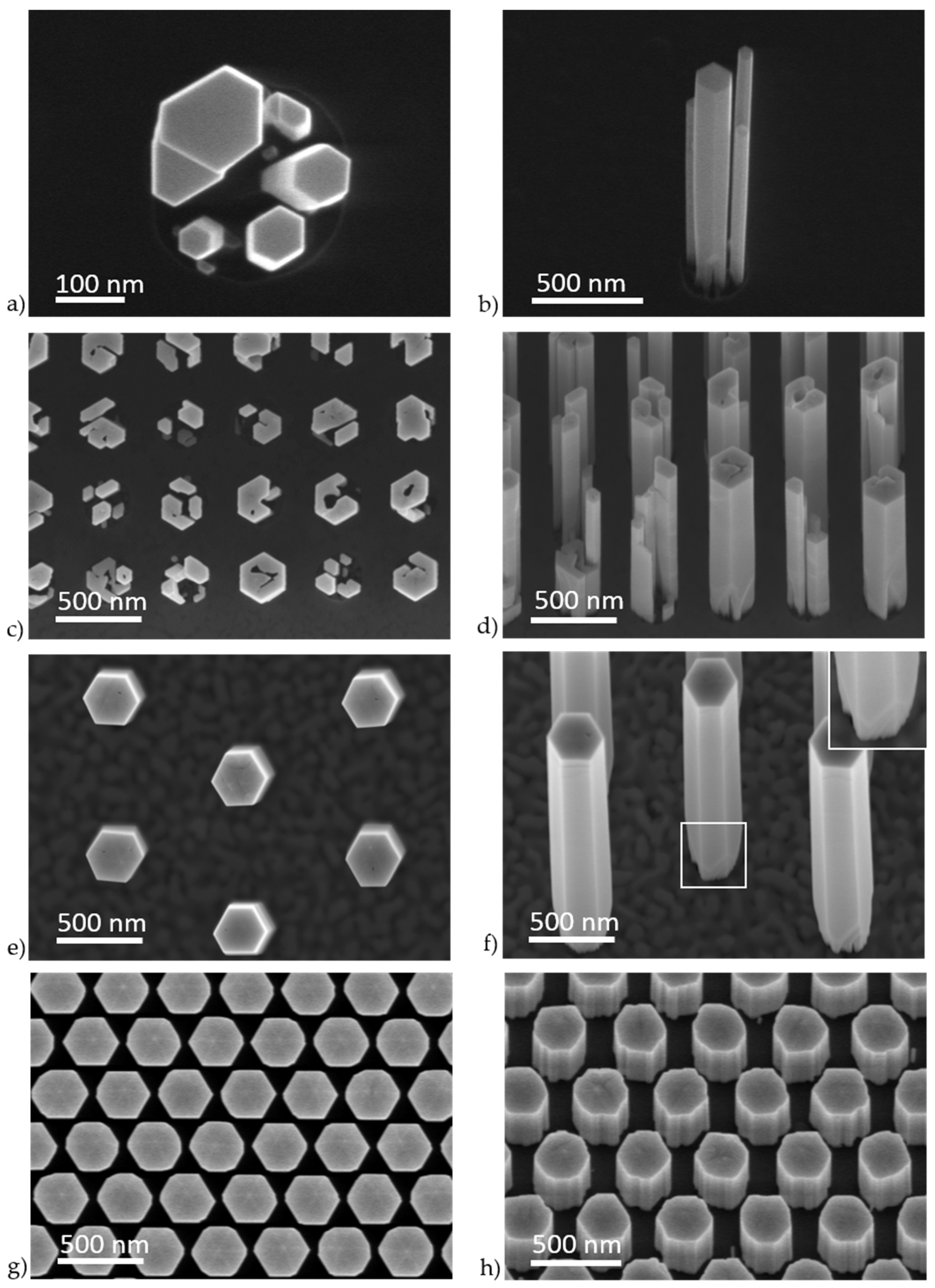
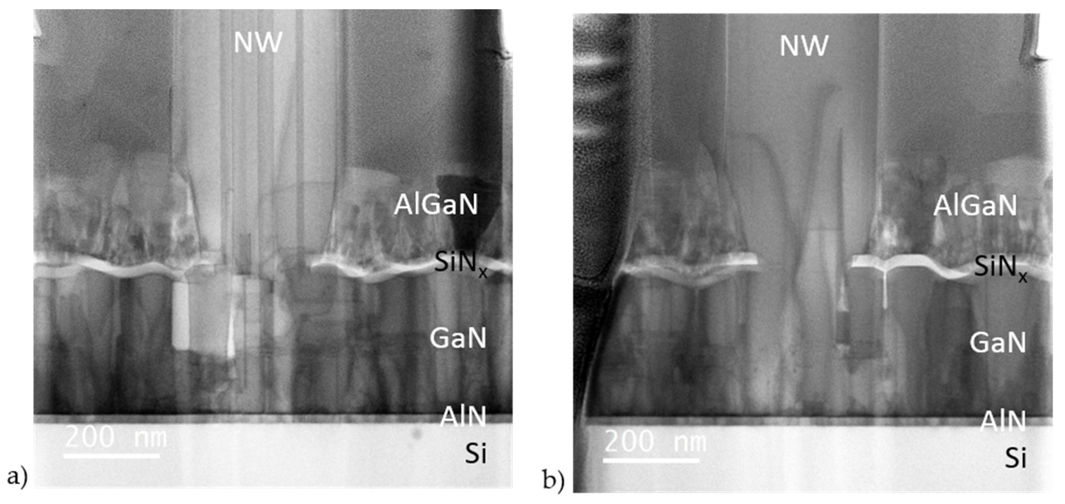
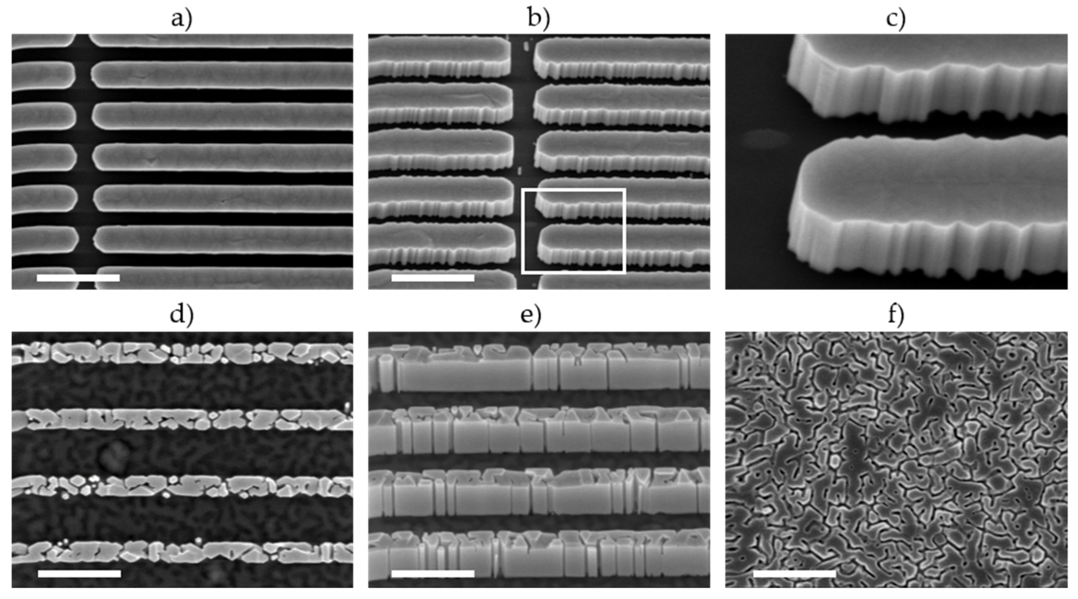
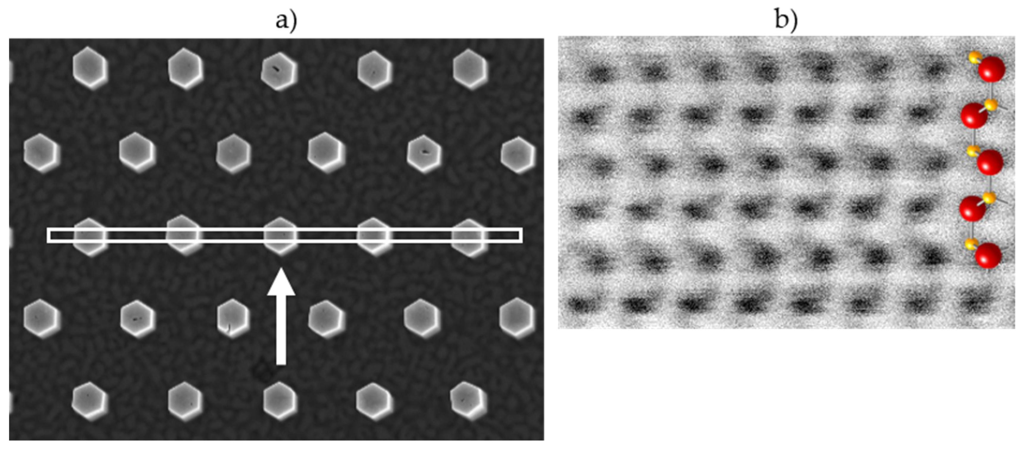
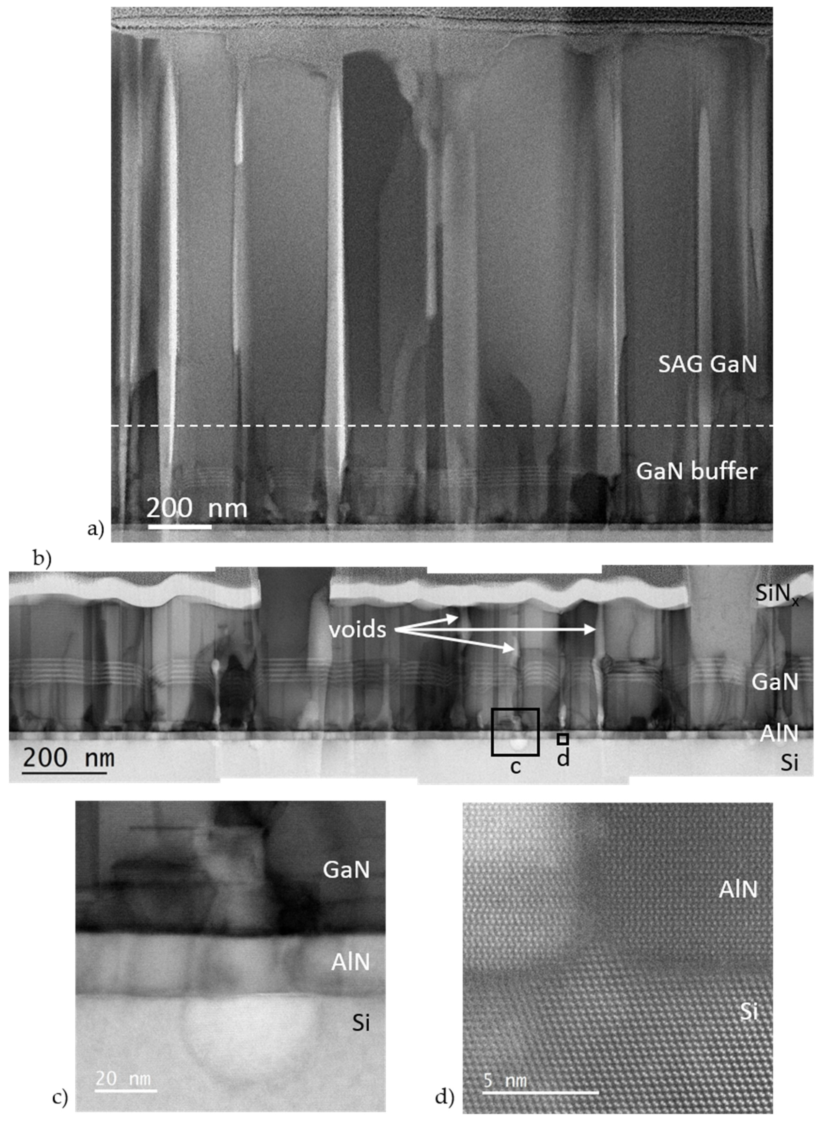
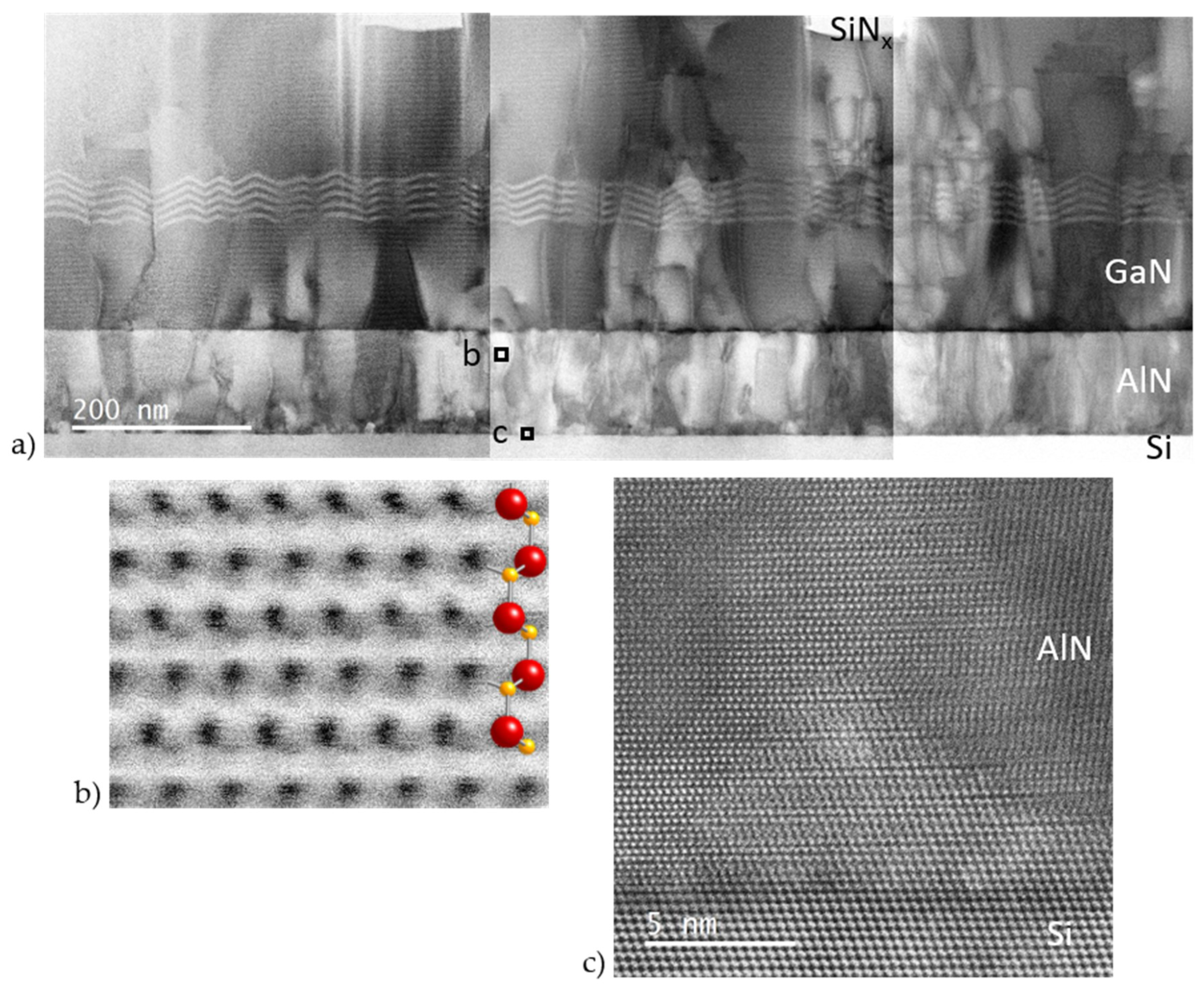
3. Results
4. Conclusions
Author Contributions
Funding
Conflicts of Interest
References
- Sanchez-Garcia, M.A.; Albert, S.; Bengoechea-Encabo, A.; Barbagini, F.; Calleja, E. Selective area growth of gan nanowires by plasma-assisted molecular beam epitaxy. In Wide Band Gap Semiconductor Nanowires for Optical Devices: Low-dimensionality Related Effects and Growth; Consonni, V., Feuillet, G., Eds.; Wiley: Somerset, NJ, USA, 2014; pp. 215–243. [Google Scholar]
- Kishino, K.; Ishizawa, S. Selective-area growth of GaN nanocolumns on Si(111) substrates for application to nanocolumn emitters with systematic analysis of dislocation filtering effect of nanocolumns. Nanotechnology 2015, 26, 225602. [Google Scholar] [CrossRef] [PubMed]
- Yamano, K.; Kishino, K.; Sekiguchi, H.; Oto, T.; Wakahara, A.; Kawakami, Y. Novel selective area growth (SAG) method for regularly arranged AlGaN nanocolumns using nanotemplates. J. Cryst. Growth 2015, 425, 316–321. [Google Scholar] [CrossRef]
- Albert, S.; Bengoechea-Encabo, A.; Sanchez-Garcia, M.A.; Kong, X.; Trampert, A.; Calleja, E. Selective area growth of In(Ga)N/GaN nanocolumns by molecular beam epitaxy on GaN-buffered Si(111): From ultraviolet to infrared emission. Nanotechnology 2013, 24, 175303. [Google Scholar] [CrossRef] [PubMed]
- Brubaker, M.D.; Duff, S.M.; Harvey, T.E.; Blanchard, P.T.; Roshko, A.; Sanders, A.W.; Sanford, N.A.; Bertness, K.A. Polarity-controlled GaN/AlN nucleation layers for selective-area growth of GaN nanowire arrays on Si(111) substrates by molecular beam epitaxy. Cryst. Growth Des. 2016, 16, 596–604. [Google Scholar] [CrossRef]
- Brubaker, M.D.; Roshko, A.; Blanchard, P.T.; Harvey, T.E.; Sanford, N.A.; Bertness, K.A. Spontaneous growth of GaN nanowire nuclei on N- and Al-polar AlN: A piezoresponse force microscopy study of crystallographic polarity. Mater. Sci. Semicond. Process. 2016, 55, 67–71. [Google Scholar] [CrossRef]
- Blanchard, P.; Brubaker, M.; Harvey, T.; Roshko, A.; Sanford, N.; Weber, J.; Bertness, K. Characterization of sub-monolayer contaminants at the regrowth interface in GaN nanowires grown by selective-area molecular beam epitaxy. Crystals 2018, 8, 178. [Google Scholar] [CrossRef]
- Cullity, B.D. Elements of X-ray Diffraction, 2nd ed.; Addison-Wesley Publishing: Reading, MA, USA, 1978. [Google Scholar]
- Darakchieva, V.; Paskova, T.; Paskov, P.P.; Monemar, B.; Ashkenov, N.; Schubert, M. Structural characteristics and lattice parameters of hydride vapor phase epitaxial GaN free-standing quasisubstrates. J. Appl. Phys. 2005, 97, 013517. [Google Scholar] [CrossRef]
- Yim, W.M.; Paff, R.J. Thermal expansion of aln, sapphire, and silicon. J. Appl. Phys. 1974, 45, 1456–1457. [Google Scholar] [CrossRef]
- Bourret, A.; Barski, A.; Rouviere, J.L.; Renaud, G.; Barbier, A. Growth of aluminum nitride on (111) silicon: Microstructure and interface structure. J. Appl. Phys. 1998, 83, 2003–2009. [Google Scholar] [CrossRef]
- Meng, W.J.; Sell, J.A.; Perry, T.A.; Rehn, L.E.; Baldo, P.M. Growth of aluminum nitride thin films on Si(111) and Si(001): Structural characteristics and development of intrinsic stresses. J. Appl. Phys. 1994, 75, 3446–3455. [Google Scholar] [CrossRef]
- Liu, R.; Ponce, F.A.; Dadgar, A.; Krost, A. Atomic arrangement at the AlN/Si (111) interface. Appl. Phys. Lett. 2003, 83, 860–862. [Google Scholar] [CrossRef]
- Schenk, H.P.D.; Kaiser, U.; Kipshidze, G.D.; Fissel, A.; Kraußlich, J.; Hobert, H.; Schulze, J.; Richter, W. Growth of atomically smooth AlN films with a 5:4 coincidence interface on Si(111) by MBE. Mater. Sci. Eng. B 1999, 59, 84–87. [Google Scholar] [CrossRef]
- Stevens, K.S.; Kinniburgh, M.; Schwartzman, A.F.; Ohtani, A.; Beresford, R. Demonstration of a silicon field-effect transistor using AlN as the gate dielectric. Appl. Phys. Lett. 1995, 66, 3179–3181. [Google Scholar] [CrossRef]
- Consonni, V.; Knelangen, M.; Geelhaar, L.; Trampert, A.; Riechert, H. Nucleation mechanisms of epitaxial GaN nanowires: Origin of their self-induced formation and initial radius. Phys. Rev. B 2010, 81, 085310. [Google Scholar] [CrossRef]
- Furtmayr, F.; Vielemeyer, M.; Stutzmann, M.; Arbiol, J.; Estradé, S.; Peirò, F.; Morante, J.R.; Eickhoff, M. Nucleation and growth of GaN nanorods on Si (111) surfaces by plasma-assisted molecular beam epitaxy—The influence of Si- and Mg-doping. J. Appl. Phys. 2008, 104, 034309. [Google Scholar] [CrossRef]
- Knelangen, M.; Consonni, V.; Trampert, A.; Riechert, H. In situ analysis of strain relaxation during catalyst-free nucleation and growth of GaN nanowires. Nanotechnology 2010, 21, 245705. [Google Scholar] [CrossRef] [PubMed]
- Landré, O.; Bougerol, C.; Renevier, H.; Daudin, B. Nucleation mechanism of GaN nanowires grown on (111) Si by molecular beam epitaxy. Nanotechnology 2009, 20, 415602. [Google Scholar] [CrossRef] [PubMed]
- Landré, O.; Fellmann, V.; Jaffrennou, P.; Bougerol, C.; Renevier, H.; Daudin, B. Growth mechanism of catalyst-free [0001] GaN and AlN nanowires on Si by molecular beam epitaxy. Phys. Status Solidi C 2010, 7, 2246–2248. [Google Scholar] [CrossRef]
- Ristić, J.; Calleja, E.; Fernández-Garrido, S.; Cerutti, L.; Trampert, A.; Jahn, U.; Ploog, K.H. On the mechanisms of spontaneous growth of III-nitride nanocolumns by plasma-assisted molecular beam epitaxy. J. Cryst. Growth 2008, 310, 4035–4045. [Google Scholar] [CrossRef]
- Gačević, Z.; Gomez Sanchez, D.; Calleja, E. Formation mechanisms of GaN nanowires grown by selective area growth homoepitaxy. Nano Lett. 2015, 15, 1117–1121. [Google Scholar] [CrossRef] [PubMed]
- De Yoreo, J.J. Principles of crystal nucleation and growth. Rev. Mineral. Geochem. 2003, 54, 57–93. [Google Scholar] [CrossRef]
- Flemings, M.C. Solidification Processing; McGraw-Hill: New York, NY, USA, 1974; p. 364. [Google Scholar]
- Zywietz, T.; Neugebauer, J.; Scheffler, M. Adatom diffusion at GaN (0001) and (0001) surfaces. Appl. Phys. Lett. 1998, 73, 487–489. [Google Scholar] [CrossRef]
- Auzelle, T.; Haas, B.; Minj, A.; Bougerol, C.; Rouvière, J.-L.; Cros, A.; Colchero, J.; Daudin, B. The influence of AlN buffer over the polarity and the nucleation of self-organized GaN nanowires. J. Appl. Phys. 2015, 117, 245303. [Google Scholar] [CrossRef]
- Roshko, A.; Brubaker, M.D.; Blanchard, M.D.; Bertness, K.A.; Harvey, T.E.; Geiss, R.H.; Levin, I. Comparison of convergent beam electron diffraction and annular bright field atomic imaging for GaN polarity determination. J. Mater. Res. 2016, 32, 936–946. [Google Scholar] [CrossRef]
- de la Mata, M.; Magen, C.; Gazquez, J.; Utama, M.I.; Heiss, M.; Lopatin, S.; Furtmayr, F.; Fernandez-Rojas, C.J.; Peng, B.; Morante, J.R.; et al. Polarity assignment in ZnTe, GaAs, ZnO, and GaN-AlN nanowires from direct dumbbell analysis. Nano Lett. 2012, 12, 2579–2586. [Google Scholar] [CrossRef] [PubMed]
- Chen, X.J.; Perillat-Merceroz, G.; Sam-Giao, D.; Durand, C.; Eymery, J. Homoepitaxial growth of catalyst-free GaN wires on N-polar substrates. Appl. Phys. Lett. 2010, 97, 151909. [Google Scholar] [CrossRef]
- Urban, A.; Malindretos, J.; Klein-Wiele, J.H.; Simon, P.; Rizzi, A. Ga-polar GaN nanocolumn arrays with semipolar faceted tips. New J. Phys. 2013, 15, 1–13. [Google Scholar] [CrossRef]
- Aseev, P.; Gačević, Ž.; Torres-Pardo, A.; González-Calbet, J.M.; Calleja, E. Improving optical performance of GaN nanowires grown by selective area growth homoepitaxy: Influence of substrate and nanowire dimensions. Appl. Phys. Lett. 2016, 108, 253109. [Google Scholar] [CrossRef]
- Gilmer, G.H.; Grabow, M.H. Models of thin film growth modes. J. Met. 1987, 39, 19–23. [Google Scholar] [CrossRef]
- Kong, X.; Li, H.; Albert, S.; Bengoechea-Encabo, A.; Sanchez-Garcia, M.A.; Calleja, E.; Draxl, C.; Trampert, A. Titanium induced polarity inversion in ordered (In,Ga)N/GaN nanocolumns. Nanotechnology 2016, 27, 065705. [Google Scholar] [CrossRef] [PubMed]
- Ruterana, P.; Sanchez, A.M.; Nouet, G. Nitride Semiconductors; Wiley VCH: Weinheim, Germany, 2003; p. 661. [Google Scholar]
- Sanchez, A.M.; Dimitrakopoulos, G.P.; P Ruterana, P. Mechanisms for the Formation of Inversion Domains in GaN; IOP Publishing Ltd.: Bristol, UK, 2004; Volume 180, p. 4. [Google Scholar]
- Coulon, P.-M.; Alloing, B.; Brändli, V.; Vennéguès, P.; Leroux, M.; Zúñiga-Pérez, J. Dislocation filtering and polarity in the selective area growth of GaN nanowires by continuous-flow metal organic vapor phase epitaxy. Appl. Phys. Express 2016, 9, 1–4. [Google Scholar] [CrossRef]
- Dreyer, C.E.; Janotti, A.; Van de Walle, C.G. Absolute surface energies of polar and nonpolar planes of GaN. Phys. Rev. B 2014, 89, 081305. [Google Scholar] [CrossRef]
- Jindal, V.; Shahedipour-Sandvik, F. Theoretical prediction of GaN nanostructure equilibrium and nonequilibrium shapes. J. Appl. Phys. 2009, 106, 083115. [Google Scholar] [CrossRef]
- Neugebauer, J. Ab initio analysis of surface structure and adatom kinetics of group-III nitrides. Phys. Status Solidi B 2001, 227, 93–114. [Google Scholar] [CrossRef]
- Northrup, J.E.; Neugebauer, J. Theory of GaN and surfaces. Phys. Rev. B 1996, 53, R10477. [Google Scholar]
- Trampert, A.; Kong, X.; Luna, E.; Grandal, J.; Jenichen, B. Microstructure of group III-N nanowires. In Wide Band Gap Semiconductor Nanowires for Optical Devices: Low-dimensionality Related Effects and Growth; Consonni, V., Feuillet, G., Eds.; Wiley: Somerset, NJ, USA, 2014; pp. 125–156. [Google Scholar]
- Consonni, V. Self-induced growth of GaN nanowires by plasma-assisted molecular beam epitaxy. In Wide Band Gap Semiconductor Nanowires for Optical Devices: Low-dimensionality Related Effects and Growth; Consonni, V., Feuillet, G., Eds.; Wiley: Somerset, NJ, USA, 2014; pp. 177–213. [Google Scholar]
- Shen, X.Q.; Ide, T.; Cho, S.H.; Shimizu, M.; Hara, S.; Okumura, H. Stability of N- and Ga-polarity GaN surfaces during the growth interruption studied by reflection high-energy electron diffraction. Appl. Phys. Lett. 2000, 77, 4013–4015. [Google Scholar] [CrossRef]
- Murray, J.L.; McAIister, A.J. The Al-Si (aluminum-silicon) system. Bull. Alloy Phase Diagr. 1994, 5, 74–84. [Google Scholar] [CrossRef]
- Adelmann, C.; Brault, J.; Mula, G.; Daudin, B.; Lymperakis, L.; Neugebauer, J. Gallium adsorption on (0001) GaN surfaces. Phys. Rev. B 2003, 67, 165419. [Google Scholar] [CrossRef]
- Neugebauer, J.; Zywietz, T.K.; Scheffler, M.; Northrup, J.E.; Chen, H.; Feenstra, R.M. Adatom kinetics on and below the surface: The existence of a new diffusion channel. Phys. Rev. Lett. 2003, 90, 056101. [Google Scholar] [CrossRef] [PubMed]
- Northrup, J.E.; Neugebauer, J.; Feenstra, R.M.; Smith, A.R. Structure of GaN(0001): The laterally contracted Ga bilayer model. Phys. Rev. B 2000, 61, 9932–9935. [Google Scholar] [CrossRef]
- Ruterana, P. Convergent beam electron diffraction investigation of inversion domains in GaN. J. Alloys Compd. 2005, 401, 199–204. [Google Scholar] [CrossRef]
- Daudin, B.; Rouvière, J.L.; Arley, M. Polarity determination of GaN films by ion channeling and convergent beam electron diffraction. Appl. Phys. Lett. 1996, 69, 2480–2482. [Google Scholar] [CrossRef]
- Daudin, B.; Rouvière, J.L.; Arley, M. The key role of polarity in the growth process of (0001) nitrides. Mater. Sci. Eng. B 1997, 43, 157–160. [Google Scholar] [CrossRef]
- Rouviere, J.L.; Weyher, J.L.; Seelmann-Eggebert, M.; Porowski, S. Polarity determination for GaN films grown on (0001) sapphire and high-pressure-grown GaN single crystals. Appl. Phys. Lett. 1998, 73, 668–670. [Google Scholar] [CrossRef]


| Sample 1 | Substrate/Buffer | AlN (nm) | GaN Buffer (nm) | SiNx (nm) | Buffer ao 2 (nm) | Δao mismatch (%) 3 |
|---|---|---|---|---|---|---|
| N-Al | Si(111)/AlN | 40 ± 5 | 0 | 74 | 0.3115 ± 0.0001 | 2.4 ± 0.2 |
| N-AlGa | Si(111)/AlN/GaN | 50 ± 5 | 45 ± 5 | 54 | 0.3195 ± 0.0005 | −0.18 ± 0.06 |
| N-AlGaSL-1 | Si(111)/AlN/GaN + SL | 20 ± 2 | 295 ± 15 | 25 | 0.3188 ± 0.0002 | 0.019 ± 0.002 |
| N-AlGaSL-2 | Si(111)/AlN/GaN + SL | 20 ± 2 | 305 ± 20 | 50 | 0.3189 ± 0.0001 | −0.006 ± 0.0004 |
| N-GaN | N-polar GaN | 0 | 0 | 50 | 0.3189 4 | 0 |
© 2018 by the authors. Licensee MDPI, Basel, Switzerland. This article is an open access article distributed under the terms and conditions of the Creative Commons Attribution (CC BY) license (http://creativecommons.org/licenses/by/4.0/).
Share and Cite
Roshko, A.; Brubaker, M.; Blanchard, P.; Harvey, T.; Bertness, K.A. Selective Area Growth and Structural Characterization of GaN Nanostructures on Si(111) Substrates. Crystals 2018, 8, 366. https://doi.org/10.3390/cryst8090366
Roshko A, Brubaker M, Blanchard P, Harvey T, Bertness KA. Selective Area Growth and Structural Characterization of GaN Nanostructures on Si(111) Substrates. Crystals. 2018; 8(9):366. https://doi.org/10.3390/cryst8090366
Chicago/Turabian StyleRoshko, Alexana, Matt Brubaker, Paul Blanchard, Todd Harvey, and Kris A. Bertness. 2018. "Selective Area Growth and Structural Characterization of GaN Nanostructures on Si(111) Substrates" Crystals 8, no. 9: 366. https://doi.org/10.3390/cryst8090366
APA StyleRoshko, A., Brubaker, M., Blanchard, P., Harvey, T., & Bertness, K. A. (2018). Selective Area Growth and Structural Characterization of GaN Nanostructures on Si(111) Substrates. Crystals, 8(9), 366. https://doi.org/10.3390/cryst8090366