Communication

Micro-Raman Imaging of Ferroelectric Domain Structures in the Bulk of PMN-PT Single Crystals

1
School of Natural Sciences and Mathematics, Ural Federal University, Ekaterinburg 620000, Russia
2
Electronic Materials Research Laboratory, Key Laboratory of the Ministry of Education & International Center for Dielectric Research, Xi’an Jiaotong University, Xi’an 710049, China
*
Author to whom correspondence should be addressed.
Crystals 2019, 9(2), 65; https://doi.org/10.3390/cryst9020065
Submission received: 8 January 2019 / Revised: 21 January 2019 / Accepted: 22 January 2019 / Published: 26 January 2019
(This article belongs to the Section Crystalline Materials)

Abstract

:
We demonstrate the application of confocal Raman microscopy (CRM) for nondestructive imaging of ferroelectric domains both at the surface and in the bulk of lead magnesium niobate-lead titanate (PMN-PT) ferroelectric single crystals. The studied model periodical domain structure was created at a [001] cut of tetragonal-phase PMN-PT crystal by the electron beam patterning technique. It was shown that the surface CRM domain image coincides in details with the image obtained by piezoresponse force microscopy.

1. Introduction

The multiaxial ferroelectric crystals of Pb(Mg1/3Nb2/3)O3-xPbTiO3 (PMN-xPT) family have been actively studied over the past decades as materials with record piezoelectric coefficients and electromechanical coupling factor [1,2,3]. In addition, these crystals possess very high nonlinear-optical and electro-optical coefficients (about 10 times higher than those of lithium niobate) [4,5].
The recently developed methods for achieving a single domain state [6], as well as suitable uniformity and possibility of preparing crystals of the optical quality made PMN-PT a promising object for domain engineering by creation of precise periodical domain structures [7]. Domain engineering requires nondestructive methods with high spatial resolution for inspection of the domain wall positions both at the surface and in the crystal bulk [7,8]. There are two main methods of domain structure imaging [9] in the crystal bulk: second harmonic generation microscopy (SHGM) [10,11,12,13,14,15,16,17] and confocal Raman microscopy (CRM) [8,18,19,20,21,22,23,24,25,26,27]. SHGM is based on the detection of local disturbance of the linear and nonlinear properties occurred at the domain walls, and thus only provides contrast of the domain walls [9]. A modification of SHGM, called Čerenkov-type SHGM, has been used recently for 3D domain visualization [13,16]. CRM combines the benefits of Raman spectroscopy and confocal microscopy and is based on the detection of local variation of the phonon modes in the vicinity of the domain walls [21]. The domain wall contrast is achieved by 2D representation of variations in the position and/or intensity of certain Raman lines recorded during the point-by-point scanning through the domain structure. The CRM imaging has been applied recently for domain walls visualization in uniaxial ferroelectrics lithium niobate (LiNbO3, LN) [20,21,22,27], lithium tantalate (LiTaO3, LT) [19], relaxor barium-strontium niobate (Sr0.61Ba0.39Nb2O6, SBN) [27] single crystals, and multiferroic bismuth ferrite (BiFeO3) ceramics [25].
Both methods allow obtaining a set of 2D images of domains or domain walls in the crystal bulk using layer-by-layer scanning at various depths. These images can contain information about the time evolution of the domain structure at the polar surface [8,19].
However, since the absolute orientation of the polarization in individual domains cannot be extracted from SHGM [11], the domain imaging in multiaxial ferroelectric is challenging due to possible existence of various types of domain walls, whereas CRM allows separating different kinds of domains by choosing an appropriate part of the spectrum [28,29]. Moreover, SHGM imaging is restricted to a certain wavelength regime [11], thus making CRM the more universal method, despite its insufficiently low time resolution for in situ measurements.
In the present paper, we demonstrate the application of the CRM technique for domain imaging at the surface and in the crystal bulk for studying the model structure of periodical c-domains with 180° walls created by the electron beam patterning technique in tetragonal-phase PMN-PT crystal.

2. Materials and Methods

The studied PMN-39PT single crystals grown by the modified Bridgman technique [30] represent the tetragonal phase at room temperature. The bulk single crystal was diced into small plates (5 × 8 × 1 mm3) perpendicular to the [001] direction with sides parallel to (010) and (100) planes. The mechanically polished samples were annealed at 750 °C for 10 h followed by slow cooling with rate 0.05–1 °C/min. This temperature treatment allowed releasing the 90°-domain-induced strain, as well as crystal growth and machining stresses to avoid crystal crack during the poling process [7]. Single-domain state has been successfully achieved at 120–230 °C by application of 2–4 kV/cm field along the [001] direction using silver paste electrodes [7], which were removed after completion of the poling process. The final optical grade mechanochemical polishing was realized using silica compound SF1 suspension by PM5 (Logitech Ltd. Glazgow, UK) polishing machine. This step is of crucial importance since any scratches occurred at the polar surfaces represent the field concentrators stimulating the domain’s nucleation, thus hampering the study of domain growth.
The studied model periodical c-domain structure with 180° walls with 10-μm period was created by electron beam (e-beam) poling technique [31,32,33] by means of a scanning electron microscope (Auriga CrossBeam Workstation, Carl Zeiss NTS GmbH, Oberkochen, Germany) with Schottky field emission gun equipped with an e-beam lithography (EBL) system (Elphy Multibeam, Raith GmbH, Manufacturer, Dortmund, Germany). The irradiated patterns were specified by Raith Nanosuite software. The stripe exposure mode of meander-scan covering of the rectangular area was used. Before e-beam poling, the (001) surface was completely covered by solid uniform 2.5-µm-thick layer of negative e-beam resist AZ nLOF 2020 (MicroChemicals GmbH, Ulm, Germany) deposited by an SM-180 spin coater (Sawatec AG, Sax, Switzerland). The opposite surface was sputtered by a 100-nm-thick Cu electrode and grounded during irradiation. The resist layer and electrode were completely chemically removed after termination of irradiation.
The surface domain structure was imaged by piezoresponse force microscopy (PFM) using built-in electronics of NTEGRA Aura (NT-MDT SI, Zelenograd, Russia) with silicon NSC-18 tips (MikroMasch, Sofia, Bulgaria). The tips had a conductive platinum coating and typical curvature radius of about 25 nm. The AC modulation voltage with amplitude Umod = 2–4 V and frequency fmod = 440 kHz (just below the tip resonance) was applied between the tip and the bottom electrode to invoke the piezoelectric response [34].
Polarized Raman spectra of PMN-PT single crystal (Manufacturer, City, Country) were measured using confocal Raman microscope Alpha 300 AR (WiTec GmbH, Ulm, Germany) equipped by solid-state laser with wavelength 488 nm and maximum power 27 mW. The direction of laser polarization was set by the half-wavelength plate placed just at the entrance of the microscope. Laser radiation was focused at the sample surface with a ×100 objective with numerical aperture (NA) 0.75. The sample was mounted at the piezoelectric stage providing the three-axis movement with few nanometer steps. Scattered light was collected by the same objective in backscattering geometry and passed through the appropriate edge-filter intercepting the Raman spectra below 100 cm−1. The separation of the polarization component in the scattered light was done by analyzer placed before a 50 μm diameter multimode optical fiber acting as a confocal pinhole. The light passing through the fiber was expanded into the spectrum by diffraction grating with 1800 grids per mm. The spectrum was detected by Andor Newton CCD camera with a 1600 × 200 pixel matrix thermoelectrically cooled down to −60 °C. The spectral resolution was about 1.2 cm−1.

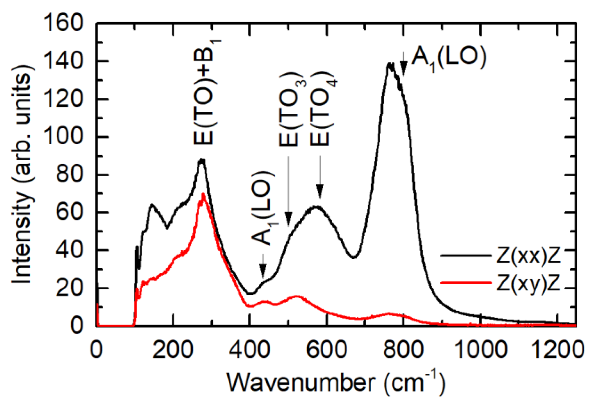
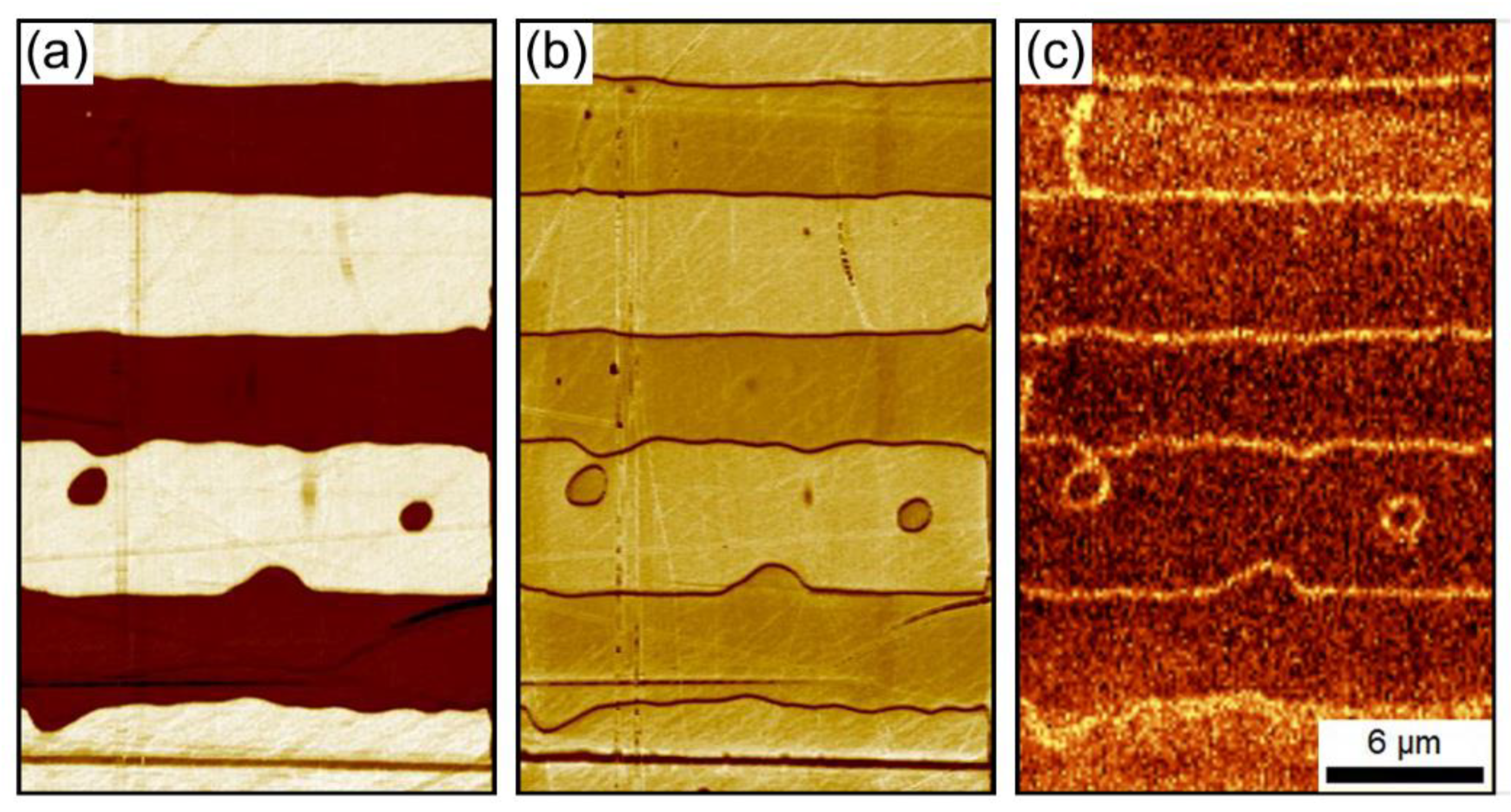
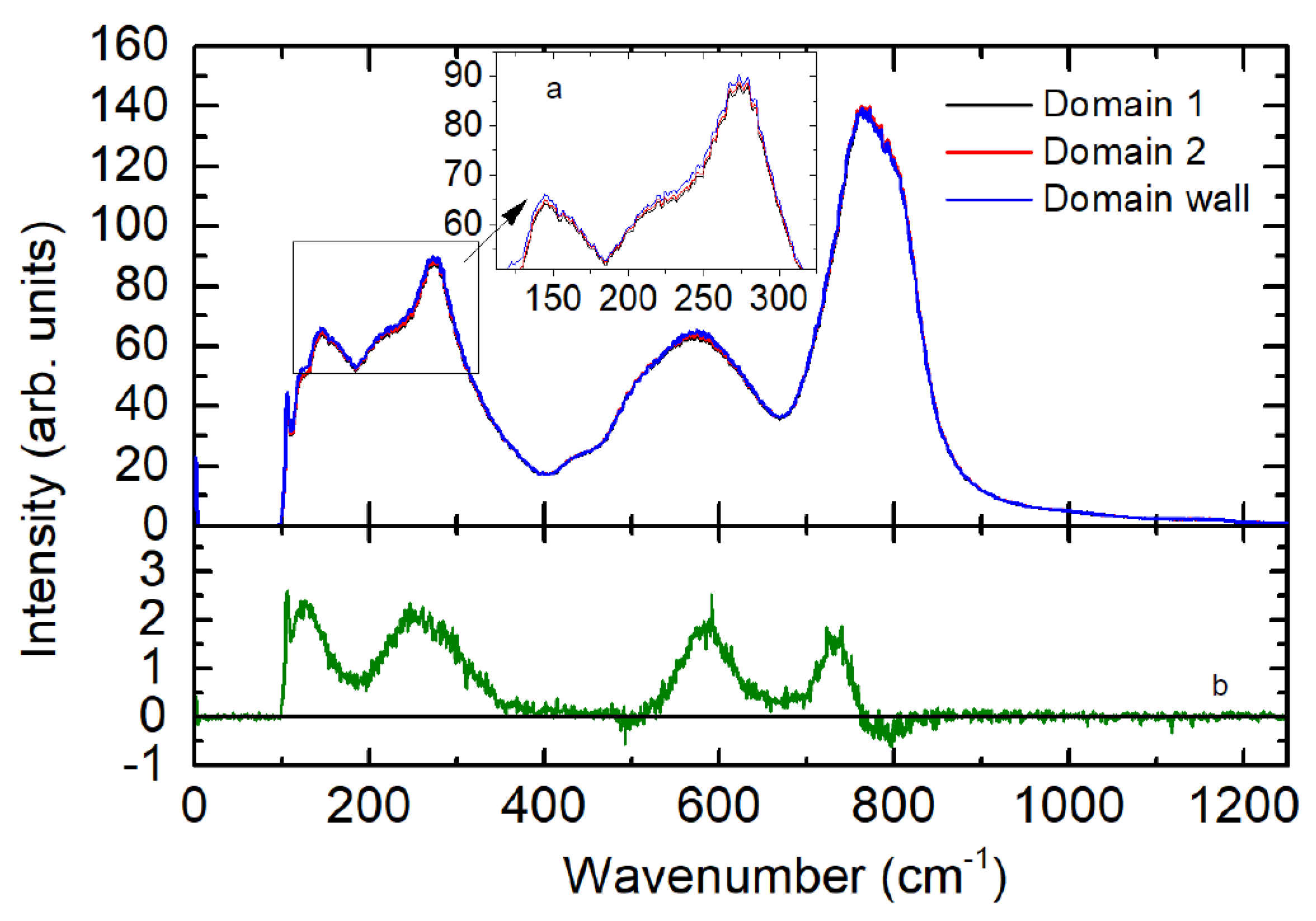
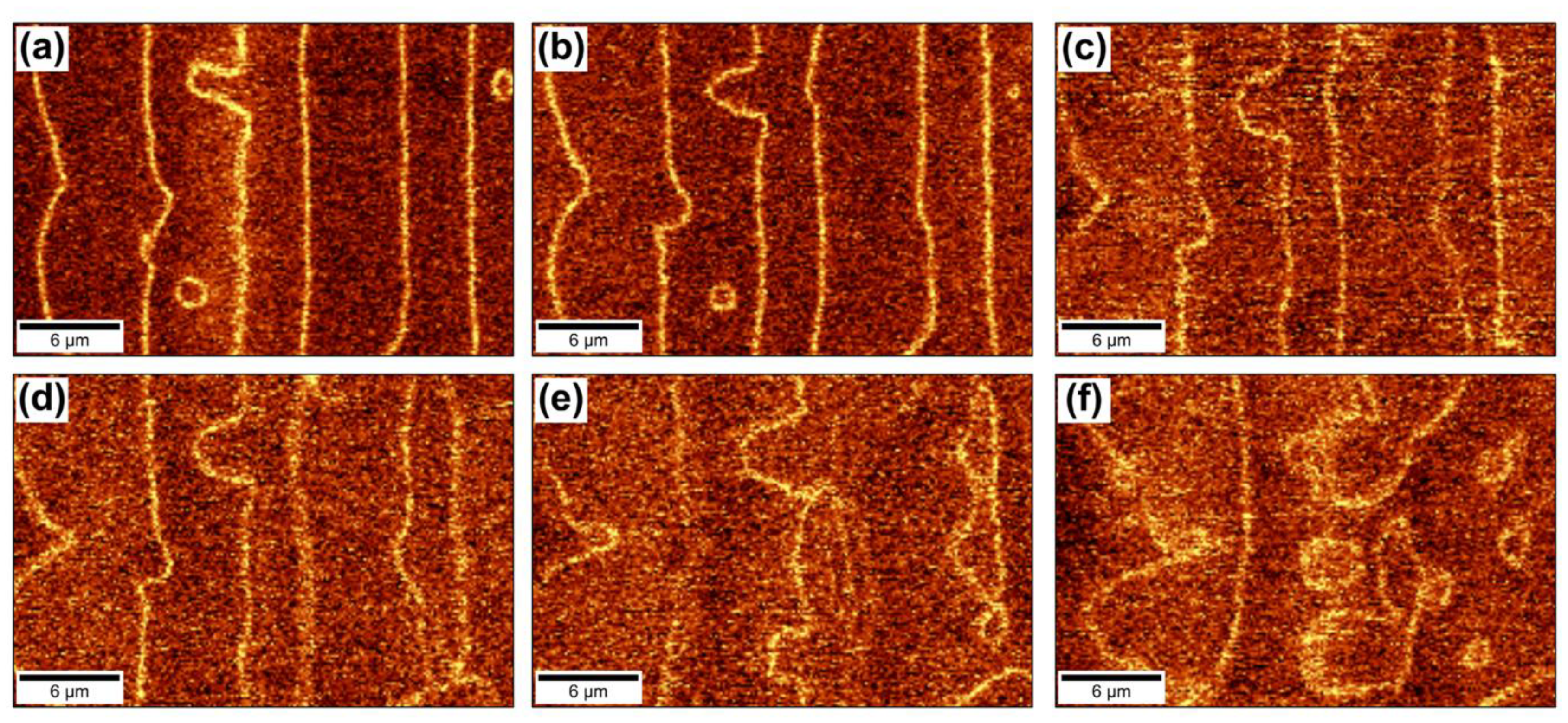
3. Results and Discussion

In the tetragonal P4mm phase, the PMN-PT crystal possesses eight Raman active vibrational modes: 3A1 + B1 + 4E. Typical polarized Raman spectra of PMN-PT crystal in Z(xx)Z and Z(xy)Z configurations after background subtraction and normalization over the total area of the spectrum are presented in Figure 1. Raman selection rules predict that Z(xx)Z spectrum consists of A1(LO) and B1 vibrational modes, whereas in Z(xy)Z configuration, only Raman inactive B2 modes should be present. However, the structural disorder inherent to PMN-PT solid solution breaks the selection rules and A1(LO) and B1 modes as well as E(TO) modes became apparent in both spectra.
The attribution of the spectral lines can be found in [35]. The spectral line A1(LO) located at 800 cm−1 is associated with stretching vibrations of Nb–O–Mg and B-cations. Line E(TO4) at 580 cm−1 is assigned to bending vibrations of oxygen octahedra, whereas line E(TO3) at 500 cm−1 is due to Nb–O–Nb stretching vibrations. Line A1(LO) located at 433 cm−1 originates from stretching vibrations of Mg–O–Mg. The spectral line located at 270 cm−1 is a mixed mode E(TO) + B1, which represents stretching vibrations of oxygen octahedra around B-cations.
The domain imaging technique was developed on the model domain structure mentioned above at room temperature. Preliminary PFM images of the domain structure at the surface are presented in Figure 2a,b. It is worth noting that no relief corresponding to the studied domain structure was found at the crystal surface.
Z(xx)Z Raman spectra measured in adjacent domains did not reveal any noticeable difference in either position or intensities of the spectral lines (Figure 3). However, the intensity of certain spectral lines slightly varied in the vicinity of the domain walls (Figure 3a,b). The spectral lines broadened because the complex and highly disordered crystal lattice did not allow detecting their shift. No spectral variations were detected in Z(xy)Z spectra; therefore, all further measurements were performed in Z(xx)Z configuration.
By analogy with effects observed earlier in LN [20,21,22], LT [19], and SBN [27] single crystals, one can assume that the spectral variations observed in the vicinity of the domain walls are due to the influence of partially compensated (residual) depolarization field [9]. Significantly weaker effects can be related with lower value of spontaneous polarization and higher dielectric permittivity of PMN-PT with respect to LN, LT, and SBN. Nevertheless, the observed effects are sufficient for imaging the domain wall positions both at the surface and in the bulk of PMN-PT single crystals.
The domain structure was visualized in the 20 × 30 μm2 area by measuring Z(xx)Z Raman spectra in adjacent points at the crystal surface with a step 150 nm and further representing the spectral parameters sensitive to the presence of domain walls as a two-dimensional pseudo-color image. The broadening of spectral lines and smallness of their variations do not allow separating the isolated spectral components, which demonstrate the sensitivity of position, intensity, or half-width to the presence of depolarization field in the vicinity of the domain walls. Therefore, to visualize the domain wall positions, the integrated intensity in the wavenumber region from 100 to 400 cm−1 was calculated as an area under the curve and then a pseudo-color representation of its spatial distribution was constructed. The obtained image of the domain walls (bright lines) at the surface of PMN-PT crystal (Figure 2c) coincides with the PFM images (Figure 2a,b). Bright color here corresponds to points at the crystal surface where the integrated intensity is increasing due to the presence of domain walls.
CRM allows measuring the spectra and visualizing the domain walls in the bulk of PMN-PT crystal by the laser beam focusing at the given depth by moving sample or objective. It is necessary to keep in mind that the real focusing depth defined by refraction index of the crystal (2.7 for PMN-PT [36]) deviates from the nominal objective shift. It was shown that the real focusing depth is proportional to the objective shift, whereby the proportionality coefficient is close to the value of crystal’s refractive index for small confocal holes (much lower than the diameter of the objective) [37].
The images of the model stripe domain structure in PMN-PT at the different depths are presented in Figure 4 with the domain wall positions presented by bright lines. It is worth noting that the line width increases with depth due to reduction of the spatial resolution. The obtained images demonstrated the essential change of the domain shape with depth. Near the surface, the domain walls noticeably bend, whereas in the bulk, some domains break down into isolated ones.

4. Conclusions

We applied the confocal Raman microscopy technique for imaging the 180° walls of c-domain periodical structure in multiaxial ferroelectric PMN-PT in tetragonal phase. We found that the wall contrast could be observed in Z(xx)Z polarization geometry using the weak intensity variations of certain spectral lines occurred in the vicinity of the domain walls due to the influence of partially compensated (residual) depolarization field. The developed technique can be used for verifying the quality of the engineered domain structure in PMN-PT crystals.

Author Contributions

The concept of the research was conceived and designed by P.Z., D.C. and V.S.; Q.H. prepared the crystal sample; D.C., E.V. and L.G. prepared the studied domain structure in the crystal and realized its visualization by piezoresponse force microscopy; P.Z. and E.G. performed confocal Raman measurements, imaging and analysis of the spectroscopic data; P.Z., D.C. and V.S. prepared the manuscript; X.W. and V.S. performed supervision and the administration of the research.

Funding

The research was funded by Russian Foundation for Basic Research (grant 17-52-80116-BRICS_a), National Natural Science Foundation of China (grant 51761145024), Government of the Russian Federation (act 211, agreement 02.180 A03.21.0006), and Ministry of Science and Higher Education of the Russian Federation (state task No. 3.4993.2017/6.7).

Acknowledgments

The authors are grateful to Ural Center for Shared Use “Modern Nanotechnology”, Ural Federal University for access to the equipment.

Conflicts of Interest

The authors declare no conflict of interest.

References

  1. Zhang, S.; Li, F.; Jiang, X.; Kim, J.; Luo, J.; Geng, X. Advantages and challenges of relaxor-PbTiO3 ferroelectric crystals for electroacoustic transducers—A review. Prog. Mater. Sci. 2015, 68, 1–66. [Google Scholar] [CrossRef] [PubMed]
  2. Kutnjak, Z.; Petzelt, J.; Blinc, R. The giant electromechanical response in ferroelectric relaxors as a critical phenomenon. Nature 2006, 441, 956–959. [Google Scholar] [CrossRef] [PubMed]
  3. Li, F.; Zhang, S.; Yang, T.; Xu, Z.; Zhang, N.; Liu, G.; Wang, J.; Wang, J.; Cheng, Z.; Ye, Z.-G.; et al. The origin of ultrahigh piezoelectricity in relaxor-ferroelectric solid solution crystals. Nat. Commun. 2016, 7, 13807. [Google Scholar] [CrossRef] [PubMed] [Green Version]
  4. Wu, F.; Yang, B.; Sun, E.; Liu, G.; Tian, H.; Cao, W. Linear electro-optic properties of relaxor-based ferroelectric 0.24Pb(In1/2Nb1/2)O3-(0.76 − x)Pb(Mg1/3Nb2/3)O3-xPbTiO3 single crystals. J. Appl. Phys. 2013, 114, 027021. [Google Scholar] [CrossRef] [PubMed]
  5. Aillerie, M.; Fontana, M.D.; Abdi, F.; Carabatos-Nedelec, C.; Theofanous, N.; Alexakis, G. Influence of the temperature-dependent spontaneous birefringence in the electro-optic measurements of LiNbO3. J. Appl. Phys. 1989, 65, 2406. [Google Scholar] [CrossRef]
  6. Zhao, Y.; Wang, S.; Fu, X.; Zhuang, Y.; Yang, R.; Yang, Z.; Li, Z.; Xu, Z.; Wei, X. Thermal annealing and single–domain preparation in tetragonal Pb(In1/2Nb1/2)O3–Pb(Mg1/3Nb2/3)O3–PbTiO3 crystal for electro–optic and non-linear optical applications. J. Appl. Phys. 2018, 123, 084104. [Google Scholar] [CrossRef]
  7. Shur, V.Ya.; Akhmatkhanov, A.R.; Baturin, I.S. Micro- and nano-domain engineering in lithium niobate. Appl. Phys. Rev. 2015, 2, 040604. [Google Scholar] [CrossRef]
  8. Shur, V.Ya.; Zelenovskiy, P.S. Micro- and nanodomain imaging in uniaxial ferroelectrics: Joint application of optical, confocal Raman, and piezoelectric force microscopy. J. Appl. Phys. 2014, 116, 066802. [Google Scholar] [CrossRef]
  9. Soergel, E. Visualization of ferroelectric domains in bulk single crystals. Appl. Phys. B 2005, 81, 729–751. [Google Scholar] [CrossRef]
  10. Uesu, Y.; Kurimura, S.; Yamamoto, Y. New nonlinear optical microscope and its application to the observation of ferroelectric domain structure. Ferroelectrics 1995, 169, 249–257. [Google Scholar] [CrossRef]
  11. Yokota, H.; Oyama, T.; Uesu, Y. Second-harmonic-generation microscopic observations of polar state in Li-doped KTaO3 under an electric field. Phys. Rev. B 2005, 72, 144103. [Google Scholar] [CrossRef]
  12. Uesu, Y.; Yokota, H.; Kawado, S.; Kaneshiro, J.; Kurimura, S.; Kato, N. Three-dimensional observations of periodically poled domains in a LiTaO3 quasiphase matching crystal by second harmonic generation tomography. Appl. Phys. Lett. 2007, 91, 182904. [Google Scholar] [CrossRef]
  13. Sheng, Y.; Best, A.; Butt, H.-J.; Krolikowski, W.; Arie, A.; Koynov, K. Three-dimensional ferroelectric domain visualization by Čerenkov-type second harmonic generation. Opt. Express 2010, 18, 16539–16545. [Google Scholar] [CrossRef] [PubMed]
  14. Denev, S.A.; Lummen, T.T.A.; Barnes, E.; Kumar, A.; Gopalan, V. Probing ferroelectrics using optical second harmonic generation. J. Am. Ceram. Soc. 2011, 94, 2699–2727. [Google Scholar] [CrossRef]
  15. Ayoub, M.; Roedig, P.; Koynov, K.; Imbrock, J.; Denz, C. Cerenkov-type second-harmonic spectroscopy in random nonlinear photonic structures. Opt. Express 2013, 21, 8220–8230. [Google Scholar] [CrossRef]
  16. Kämpfe, T.; Reichenbach, P.; Schröder, M.; Haußmann, A.; Eng, L.M.; Woike, T.; Soergel, E. Optical three-dimensional profiling of charged domain walls in ferroelectrics by Cherenkov second-harmonic generation. Phys. Rev. B 2014, 89, 035314. [Google Scholar] [CrossRef]
  17. Ayoub, M.; Futterlieb, H.; Imbrock, J.; Denz, C. 3D imaging of ferroelectric kinetics during electrically driven switching. Adv. Mater. 2017, 29, 1603325. [Google Scholar] [CrossRef]
  18. Berth, G.; Hahn, W.; Wiedemeier, V.; Zrenner, A.; Sanna, S.; Schmidt, W.G. Imaging of the ferroelectric domain structures by confocal Raman spectroscopy. Ferroelectrics 2011, 420, 44–48. [Google Scholar] [CrossRef]
  19. Shur, V.Ya.; Zelenovskiy, P.S.; Nebogatikov, M.S.; Alikin, D.O.; Sarmanova, M.F.; Ievlev, A.V.; Mingaliev, E.A.; Kuznetsov, D.K. Investigation of the nanodomain structure formation by piezoelectric force microscopy and Raman Confocal Microscopy in LiNbO3 and LiTaO3 crystals. J. Appl. Phys. 2011, 110, 052013. [Google Scholar] [CrossRef]
  20. Zelenovskiy, P.S.; Fontana, M.D.; Shur, V.Ya.; Bourson, P.; Kuznetsov, D.K. Raman visualization of micro- and nanoscale domain structures in lithium niobate. Appl. Phys. A 2010, 99, 741–744. [Google Scholar] [CrossRef]
  21. Zelenovskiy, P.S.; Shur, V.Ya.; Bourson, P.; Fontana, M.D.; Kuznetsov, D.K.; Mingaliev, E.A. Raman study of neutral and charged domain walls in lithium niobate. Ferroelectrics 2010, 398, 34–41. [Google Scholar] [CrossRef]
  22. Zelenovskiy, P.S.; Shur, V.Ya.; Kuznetsov, D.K.; Mingaliev, E.A.; Fontana, M.; Bourson, P. Visualization of nanodomains in lithium niobate single crystals by scanning laser Confocal Raman Microscopy. Phys. Solid State 2011, 53, 109–113. [Google Scholar] [CrossRef]
  23. Rubio-Marcos, F.; Del Campo, A.; Lopez-Juarez, R.; Romeroa, J.J.; Fernandez, J.F. High spatial resolution structure of (K,Na)NbO3 lead-free ferroelectric domains. J. Mater. Chem. 2012, 22, 9714–9720. [Google Scholar] [CrossRef]
  24. Guennou, M.; Savinov, M.; Drahokoupil, J.; Luo, H.; Hlinka, J. Piezoelectric properties of tetragonal single-domain Mn-doped NBT-6%BT single crystals. Appl. Phys. A 2014, 116, 225–228. [Google Scholar] [CrossRef]
  25. Borodavka, F.; Pokorny, J.; Hlinka, J. Combined piezoresponse force microscopy and Raman scattering investigation of domain boundaries in BiFeO3 ceramics. Phase Trans. 2016, 89, 746–751. [Google Scholar] [CrossRef]
  26. Hammoum, R.; Fontana, M.D.; Bourson, P.; Shur, V.Ya. Characterization of PPLN-microstructures by means of Raman spectroscopy. Appl. Phys. A 2008, 91, 65–67. [Google Scholar] [CrossRef]
  27. Zelenovskiy, P.S.; Shikhova, V.A.; Ievlev, A.V.; Neradovskiy, M.M.; Shur, V.Ya. Micro-Raman visualization of domain structure in Strontium Barium Niobate single crystals. Ferroelectrics 2012, 439, 33–39. [Google Scholar] [CrossRef]
  28. Pezzotti, G.; Matsutani, A.; Zhu, W. Spectroscopic assessments of domain texture in barium titanate: I. confocal Raman polarization analysis. J. Am. Ceram. Soc. 2010, 93, 256–264. [Google Scholar] [CrossRef]
  29. Deluca, M.; Higashino, M.; Pezzotti, G. Raman tensor elements for tetragonal BaTiO3 and their use for in-plane domain texture assessments. Appl. Phys. Lett. 2007, 91, 091906. [Google Scholar] [CrossRef]
  30. Zhang, S.; Luo, J.; Hackenberger, W.; Shrout, T.R. Characterization of Pb(In1/2Nb1/2)O3–Pb(Mg1/3Nb2/3)O3–PbTiO3 ferroelectric crystal with enhanced phase transition temperatures. J. Appl. Phys. 2008, 104, 064106. [Google Scholar] [CrossRef]
  31. Chezganov, D.S.; Smirnov, M.M.; Kuznetsov, D.K.; Shur, V.Ya. Electron beam domain patterning of MgO-doped Lithium Niobate crystals covered by resist layer. Ferroelectrics 2015, 476, 117–126. [Google Scholar] [CrossRef]
  32. Shur, V.Ya.; Chezganov, D.S.; Akhmatkhanov, A.R.; Kuznetsov, D.K. Domain patterning by electron beam of MgO doped lithium niobate covered by resist. Appl. Phys. Lett. 2015, 106, 232902. [Google Scholar] [CrossRef]
  33. Vlasov, E.; Chezganov, D.; Chuvakova, M.; Shur, V.Ya. The ferroelectric domain structures induced by electron beam scanning in Lithium Niobate. Scanning 2018, 2018, 7809826. [Google Scholar] [CrossRef] [PubMed]
  34. Soergel, E. Piezoresponse force microscopy (PFM). J. Phys. Appl. Phys. 2011, 44, 464003. [Google Scholar] [CrossRef]
  35. Ge, W.; Zhu, W.; Pezzotti, G. Raman selection rules and tensor elements for PMN–0.3PT single crystal. Phys. Status Solidi B 2009, 246, 1340–1344. [Google Scholar] [CrossRef]
  36. Chan, K.Y.; Tsang, W.S.; Mak, C.L.; Wong, K.H.; Hui, P.M. Effects of composition of PbTiO3 on optical properties of (1−x)PbMg1/3Nb2/3O3−xPbTiO3 thin films. Phys. Rev. B 2004, 69, 144111. [Google Scholar] [CrossRef]
  37. Everall, N.J. Modeling and measuring the effect of refraction on the depth resolution of Confocal Raman Microscopy. Appl. Spectrosc. 2000, 54, 773–782. [Google Scholar] [CrossRef]
Figure 1. Raman spectra of lead magnesium niobate-lead titanate (PMN-PT) single crystal for two polarizations.
Crystals 09 00065 g001
Figure 2. Images of the model domain structure at the surface of PMN-PT single crystal: (a) Piezoresponse force microscopy (PFM) phase, (b) PFM amplitude, (c) confocal Raman microscopy (CRM). CRM image represents pseudo-color representation of spatial distribution of integrated intensity in 100–400 cm−1 spectral region.
Crystals 09 00065 g002
Figure 3. (Top) Raman spectra of PMN-PT measured in adjacent domains and at the domain wall with zoom onto the low frequency region (inset) and (bottom) difference between spectra measured at the domain wall and in the domains.
Crystals 09 00065 g003
Figure 4. CRM images of the stripe domain structure in PMN-PT crystal at different depths: (a) 10 μm, (b) 20 μm, (c) 30 μm, (d) 35 μm, (e) 50 μm, and (f) 70 μm. Pseudo-color representation of spatial distribution of integrated intensity in 100–400 cm−1 spectral region.
Crystals 09 00065 g004

