Article

Effects of He+ and H+ Co-Implantation with High Energy on Blisters and Craters of Si and SiO2-On-Si Wafers

1
Institute of Laser Engineering, Beijing University of technology, Beijing 100124, China
2
College of Microelectronics, Beijing University of technology, Beijing 100124, China
*
Author to whom correspondence should be addressed.
Crystals 2019, 9(12), 671; https://doi.org/10.3390/cryst9120671
Submission received: 17 November 2019 / Revised: 4 December 2019 / Accepted: 10 December 2019 / Published: 12 December 2019

Abstract

:
In this paper, effects of He+ and H+ co-implantation with high implantation energy on surface blisters and craters at different annealing conditions are systematically investigated. Surface morphology as well as defect microstructure are observed and analyzed by various approaches, such as scanning electron microscopy (SEM), optical microscopy (OM), atomic force microscopy (AFM), and Raman spectroscopy. It is found that after 500 °C annealing and above for 1 h, surface blisters and exfoliation are observed for Si and SiO2-on-Si wafers except for the samples implanted with only He+ ions. AFM images reveal that the heights of blisters in Si and SiO2-on-Si wafers are 432 nm and 397 nm respectively and the thickness of transfer layer is at the depth of about 1.4 μm, which is consistent with the projected range of He+ and H+ ions. Raman spectroscopy demonstrates that higher annealing temperature can lead to a stronger intensity of the VH2 peak. Under the same implantation parameters, surface morphology of Si and SiO2-on-Si wafers is different after annealing process. This phenomenon is discussed in detail.

1. Introduction

Implantation of light ions such as hydrogen and helium into semiconductors contributes to the blisters of free surface and defect microstructures of materials. Based on such phenomenon, the Smart CutTM technology has been invented by Bruel to transfer a thin Si layer from a donor substrate to a handling substrate, leading to the production of high-quality silicon-on-insulator (SOI) wafers [1,2,3]. Many studies have provided evidence for the fact that after implantation and followed annealing, vacancies and hydrogen atoms in silicon can precipitate into nanoscale or microscale platelets and then grow up at length according to Ostwald ripening theory [4,5]. During the annealing, these platelets eventually evolve into micro-cracks by mechanical coalescence [6,7]. When these micro-cracks reach the free surface of the wafer, stress generated by pressure inside the platelets can relax through the blisters of the surface [8,9]. These blisters then give rise to the exfoliation of the surface.
He+ is chemically inactive and coprecipitates with vacancies to form bubbles because He atoms prefer to be trapped in a region containing low electron density [10]. On the other hand, H atoms diffuse to vacancy clusters in order to minimize the energy of the system by passivating the dangling bonds. Agarwal et al. [11] verified firstly that when He+ and H+ were co-implanted sequentially, thin film exfoliation was achieved by implanting a total dose at least three times smaller than that required by H+ alone. In 2013, Wang et al. [12] found the relationship between surface damage and defect microstructure in Si wafers with 220 nm top SiO2 sequentially co-implanted with 40 keV, 5 × 10¹⁶/cm2 He+ and 35 keV 5 × 10¹⁶/cm2 H+ respectively. In 2016, Cherkashin et al. [13] studied the characteristics of Si(001) wafers covered by a 25 nm-thick top SiO2 layer and compared the defect microstructures after annealing under different implantation sequences of 12 keV, 7 × 10¹⁵ He+/cm2 and 6 keV, 6 × 10¹⁵ H+/cm2. In 2018, Cherkashin et al. [14] investigated the influences of He+ and H+ relative depth distribution on blisters and exfoliation on surface with a 25 nm-thick top SiO2 layer. Since the top SiO2 layer mentioned above was relatively thin, the implantation energies of He+ and H+ ions needed were just several dozens of keV.
In this work, synergistic effects of the co-implantation of He+ and H+ with high implantation energy into the Si and SiO2-on-Si wafers are comprehensively investigated. Experiments are set up to explore the function of SiO2 layer on the Si wafer during the different implantation processes. Meanwhile, high implantation energy results in a much deeper distribution of He+ and H+ in Si wafers and SiO2-on-Si wafers, allowing us to explore the effect of implantation depth on the size and density of blisters and craters.

2. Materials and Methods

Three experiments were carried out on 500 μm p-type Czochralski-grown Si (111) substrates: sample A was implanted at room temperature with only 300 keV He+ at a dose of 5 × 10¹⁶/cm2, sample B and sample C were both sequentially implanted with 300 keV, 5 × 10¹⁵/cm2 He+ and 160 keV, 4 × 10¹⁶/cm2 H+. However, a 400 nm-thick SiO2 layer under the wet oxidation temperature of 1050 °C for 3 h was grown on the Si substrate in sample C before ion implantation. The detailed implantation parameters were shown in Table 1. To be noted, the normal axes of sample A and sample B surfaces were tilted 7° off relative to the axis of incident ion beam to minimize channeling effect. According to the simulation results of SRIM-2013 software [15] as shown in Figure 1, the implantation of 300 keV He+ and 160 keV H+ ions had approximately the same projected range (Rp) and different straggle (ΔRp) in both sample B and sample C. After implantation, each wafer was cut into four smaller specimens and then subjected into furnace annealing at 400 °C, 500 °C, 800 °C, and 1000 °C in a flow of N2 for 1 h respectively.
In order to analyze the surface morphology, GeminiSEM 300 SEM (using back-scattered electrons mode) and Olympus OM were both applied. The size of craters and blisters were measured by Bruker AFM in tapping mode. Renishaw Raman spectroscopy was also evolved to study the thermal evolution of Si-H interactions with a resolution of 2 cm−1. A 532 nm laser was used as the excitation source and laser power was fixed at 50 mW. Meanwhile, the laser beam was set to focus on the sidewall of craters so as to obtain a more distinct Raman spectrum.

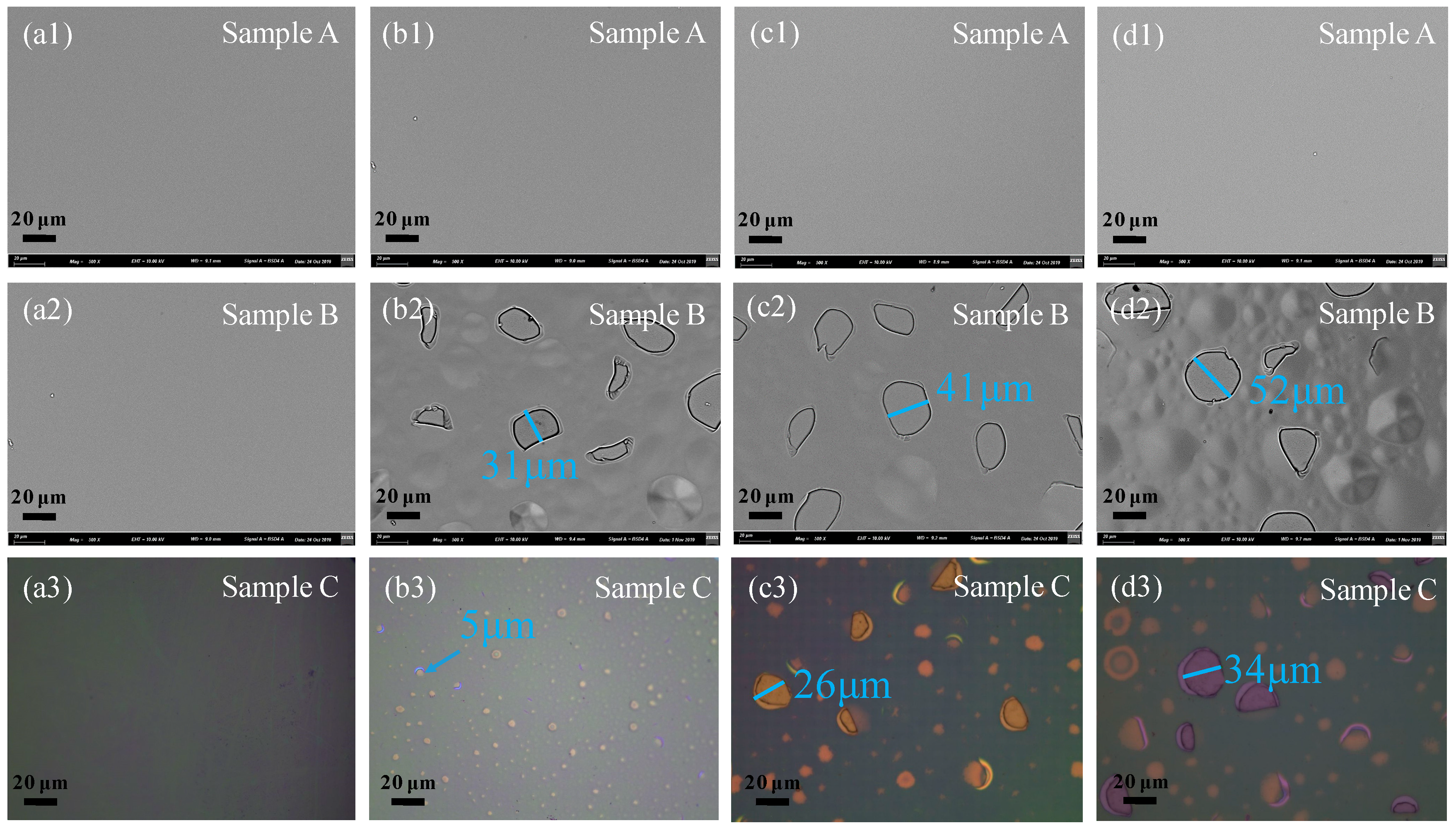
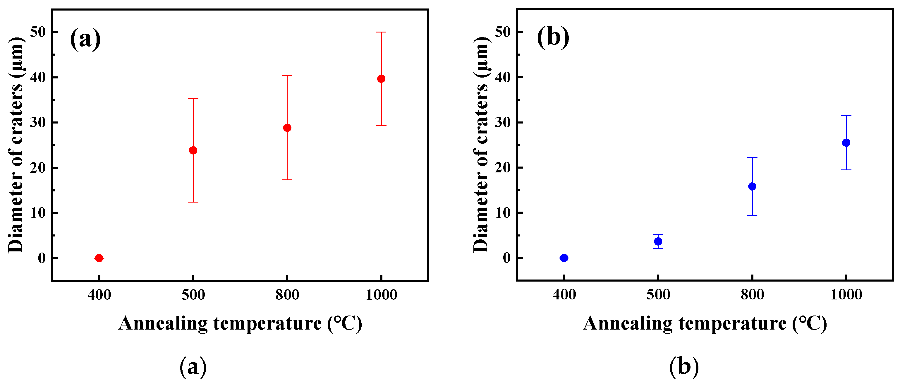
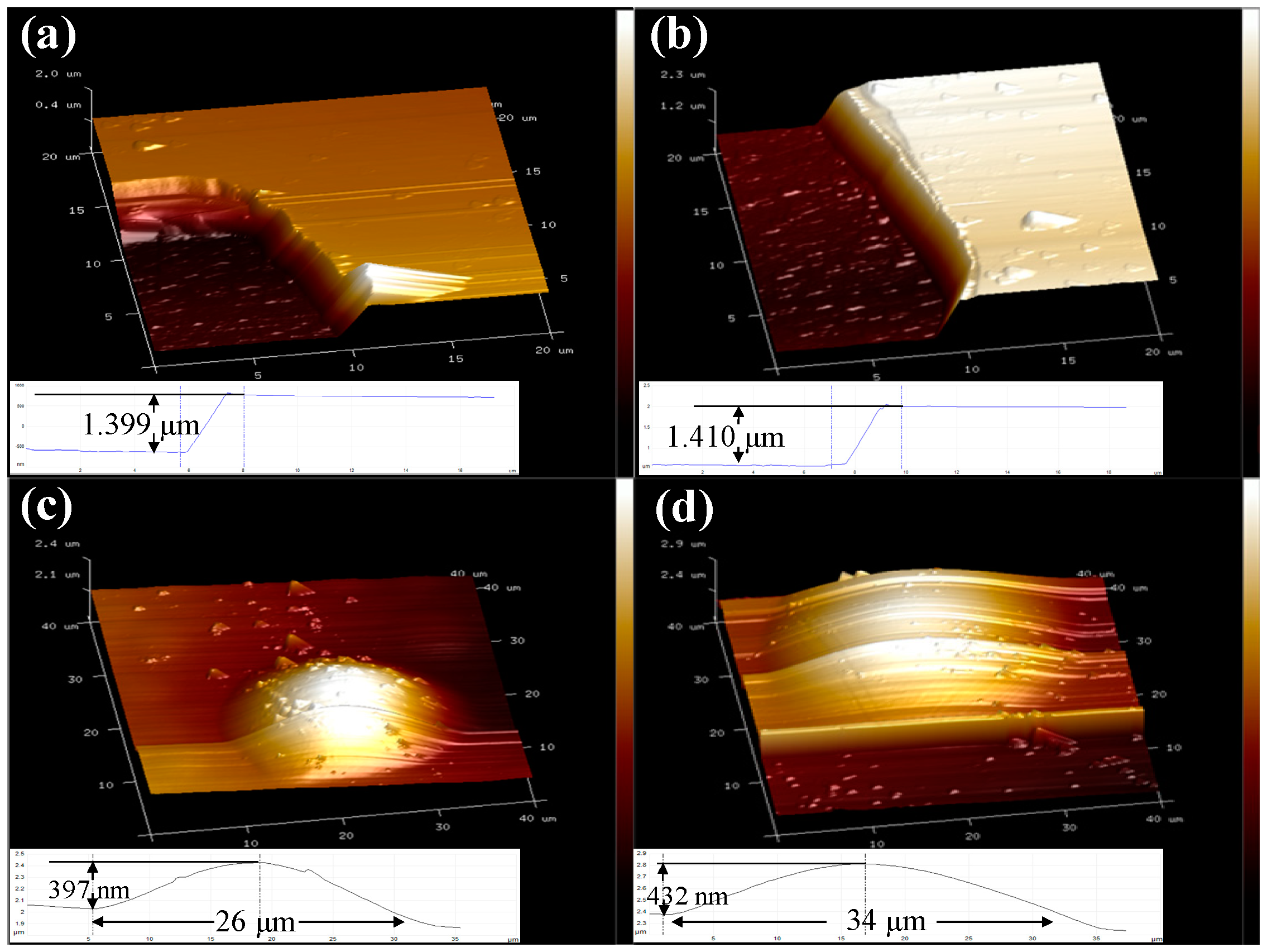
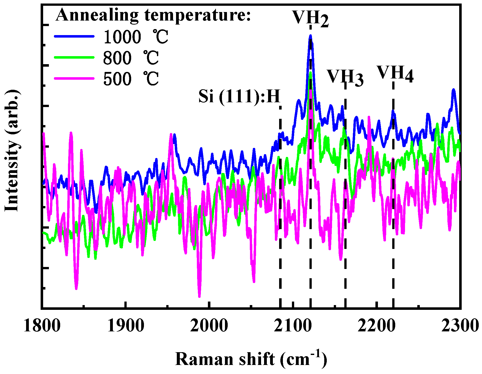
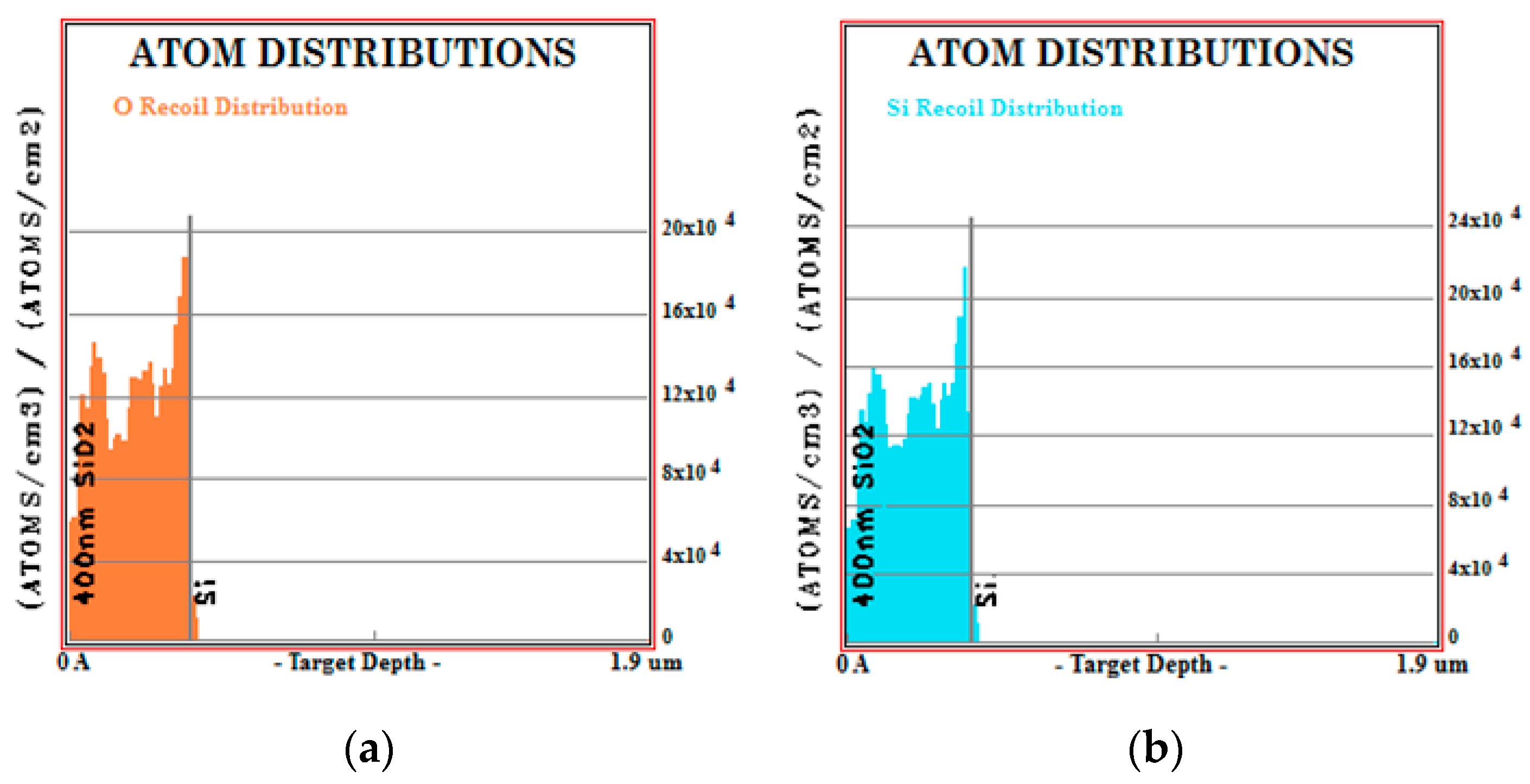
3. Experiment Results

Figure 2 shows the SEM and OM images of the sample A, sample B, and sample C after annealing at the different temperatures of 400 °C, 500 °C, 800 °C, and 1000 °C for 1 h. Because of poor conductivity of the SiO2, OM measurement was chosen to inspect the surface morphology of sample C. It was found that no surface changes (i.e., blisters and exfoliation) occurred on sample A even after 1000°C annealing for 1 h. For sample B, no blisters or craters were formed on the surface at 400 °C. However, when the annealing temperature rose from 500 to 1000 °C, surface morphology was gradually modified. The average diameter of shallow craters on sample B was measured to be several tens of microns at 500 °C and then the size became larger and larger as the temperature increased, indicating that the evolution of surface morphology closely depends on the annealing temperature. For sample C, at the beginning no changes were detected on the surface either. While the annealing temperature increases to 500 °C, blisters and craters began to appear on the SiO2 surface. The size of craters is statistically plotted in Figure 3. It is demonstrated that raising the temperature to 800 °C leads to the growth of blisters and the appearance of large craters. According to the results, quantity and size of the blisters and craters in sample C were both less than those of sample B due to the growth of SiO2 layer. Nevertheless, both samples revealed the same rule that higher annealing temperature could activate the diffusion of the gas and vacancies from small blister cavities to the bigger ones. When the stress fields of blister cavities overlap, coalescence occurs [16].
Figure 4 displays the more detailed surface features of sample B and sample C detected by AFM. A single crater is captured as shown in Figure 4a,b. Depths of the crater in two samples were measured to be 1.399 μm and 1.410 μm respectively, which is consistent with the projected range of He+ or H+ ions. Therefore, it can be speculated that the thickness of the transfer layer was about 1.4 μm. Figure 4c,d exhibits blisters on the surfaces of sample C and sample B. The heights of blisters in sample B and sample C were 432 nm and 397 nm respectively. The diameters of blisters in sample B and sample C were about 34 μm and 26 μm respectively.
Raman spectra for sample B is plotted in Figure 5. According to Ref. [17], the stretching modes for Si(111):H, VH2, VH3, and VH4 were located at 2084 cm−1, 2125 cm−1, 2164 cm−1, and 2219 cm−1, respectively. With the increase of annealing temperature, the strongest peak position gradually moved to 2125 cm−1, which presented the “VH2-like” defects, indicating that more and more H2 combined with vacancy species [18]. The defects initially generated by He and H ions co-implantation evolved into internal surfaces that eventually joined to form the macroscopic cracks, leading to cooperative shearing of a Si layer. Between 500 °C and 1000 °C, the most significant change was the decrease in the concentration of hydrogenated multi-vacancies and the concomitant increase in the absorption of VH3,4 species. This mode was assigned to “VH2-like” defects, based on its frequency. Both width and center frequency were in agreement with the isolated VH2 defect. This is consistent with the mechanism as follows:
H e   + V   + H 2   ( H e V H 2 )
Therefore, other types of peak intensity gradually became weak and the characteristic peak of VH2 was enhanced, regarded as precursors of the gas-filled platelets and blisters. The microstructures contain H2–He platelets and He bubbles, and H2-He platelets coalesce to form micro-cracks. With increase of annealing temperature, characteristic peak strength of Si(111):H is impaired gradually. This implies that blisters can merge with neighboring ones at implantation depth [19].

4. Discussion

When light ions driven by a high energy electromagnetic field are implanted into silicon through the surface of Si or SiO2, this process would cause considerable number of defects including vacancy-like defects or silicon interstitials. Since He atom is inert while H is an active element, no chemical reaction could happen between He+ and defects even though there exist a lot of lattice dislocations in sample A implanted with only He+. Moreover, a band of nanometer sized cavities is created at the depth of projected range of He+ ions after annealing and the cavities distribute quite discretely [20]. After He ions implantation and even after 1000 °C no blisters occur. After implantation and then at the beginning of the annealing, He coprecipitates with vacancies to form bubbles and in order to activate the Ostwald ripening (change of He atoms and vacancies between bubbles), it is required to overcome high activation energy [10]. However, H+ ions can readily react with lattice defects induced by ions implantation, which makes H atoms trapped in various defects. Both He+ and H+ ions implanted into samples produce vacancy-like defects at the end of their projected ranges. As shown in Figure 5, at 500 °C and above, the Raman characteristic peak of VH2 in sample B is the maximum, meaning that more H2 are trapped in vacancies. After He ions implantation the system contains Si vacancies and interstitials, He inside bubbles and He in interstitial sites [21]. Then when H+ is implanted, H+ prefers to passivate the dangling bonds, store inside vacancies, and create hydrogenated complexes rich in vacancies VnHm with n > m (at the low frequency below 2050 cm−1) and hydrogenated complexes rich in hydrogen VnHm with n < m (at the high frequency above 2050 cm−1). After annealing the complexes rich in vacancies dissociate and H vacancies diffuse to the complexes rich in hydrogen VnHm with n < m. He in interstitial sites and in very small voids as HeV1 diffuse to the complexes rich in hydrogen and then platelets form. These platelets are pressurized by H2 and He and their internal surface are passivated by H. Thus there is a synergistic effect between He and H. On the other hand, He atoms trapped in bubbles before H implantation do not diffuse and stay inside the bubbles because it is energetically expensive to take out He from bubbles. Finally the microstructure contains H2–He platelets and He bubbles and with further annealing H2–He platelets coalesce to form micro-cracks that relax to the free surface inducing blisters. During the thermal growth of He blisters, additional H atoms are trapped and evolve into H2, increasing the pressure of He blisters. Extra pressure would form strong strain surrounding blisters. The strain is able to induce deformation of the surrounding lattice atoms and propagates further in the sample. According to Ref. [22,23], when the blister diameter increases, the stress and strain which are more localized in the periphery of the blistering increase till reaching a limit of Si plasticity and then a fracture occurs. Compared with the thickness of silicon substrate material, the thickness of the implantation layer is trivial. Thus, the strain needs to release towards the surface of samples and makes the sample surface appear the blisters and the localized craters, as shown in Figure 2.
In Figure 2, the diameters of craters in sample B at 500 °C, 800 °C, and 1000 °C are 31 μm, 41 μm, and 52 μm, respectively and in sample C, at 800 °C and 1000 °C annealing temperature, the diameters of craters are 26 μm and 34 μm respectively. Formation of craters is mainly caused by burst of blisters. Mitani et al. [24] obtained the formula of critical radius of blisters at interface of Si wafers through calculation:
r c r i t = ( 16 γ p E t 3 9 α ( 1 ν 2 ) Δ p 2 ) 1 / 4 ,
where γ p is the surface energy of cavity surface passivated by H atoms, E is Young’s modulus, t is the depth of ions implantation, α is a geometrical factor of about 1/3–1/2, ν is Poisson’s ratio, and Δ p is the pressure difference between inside and outside cavity or crack. The above equation indicates that the critical size of surface blisters is proportional to the depth of ion implantation. With increase of depth of ion implantation, the diameter of blisters become large, leading to increase of diameter of craters.
However, it is interesting to find that at the same annealing temperature, the number and size of the blisters and craters in the sample C are both obviously less than those in the sample B. According to the simulation results of the SRIM-2013, the projected range of He+ and H+ ions in sample C was about 1.37 μm and 1.38 μm, respectively. Due to the existence of the top SiO2 layer, when He+ or H+ is implanted into the sample C through the SiO2 layer, the implantation energy of light ions is transferred to O and Si atoms and causes damage cascades. In Figure 6, the recoil distributions of O and Si atoms are mainly concentrated in the SiO2–Si interface and below 20 nm. O and Si atoms primarily existed in the form of interstitials. Puska et al. [25] verified that the excess of self-interstitials would be generated by the process of thermal oxidation near the SiO2/Si interface. Interstitials cannot diffuse to the surface of sample C through SiO2–Si interface and then annihilate. Thus, when He+ and H+ are implanted into the sample C, two areas with different defect types would form inside material: one is the excess of self-interstitials near the SiO2–Si interface, the other is the extra vacancy-like defects in the vicinity of the projected range of He+ and H+. After the implantation of 300keV He+ and 160 keV H+ into sample C, the distance between two regions where two defects are located is large. So the composite effect between two regions is weak, which leads to decrease of cavities growth rate in the subsequent annealing process. The band of cavities is widened due to the diffusion and recombination between vacancies and interstitials, but the average size of cavities is reduced. Moreover, the SiO2 layer can be used as the barrier to prevent the diffusion of interstitials towards the surface in the process of annealing.

5. Conclusions

In summary, the influence of He+ and H+ co-implantation on the evolution of blisters and craters is systematically evaluated. The experiment results suggest that the size of craters and the height of blisters are both positively related to the annealing temperature. The maximum diameter of the craters could reach nearly 50 μm at 1000 °C. The relationship between implantation depth and critical radius of blisters and craters is also theoretically analyzed. With the increase of implantation depth, the diameter of blisters become larger, leading to increase of diameter of craters. In addition, it is also demonstrated that due to the deep implantation caused by high implantation energy, the self-interstitial near the SiO2–Si interface has a weak composite effect on the vacancy-like defects at the projected range. As a result, quantities and size of blisters and craters in SiO2-on-Si wafer are both less than these in Si wafer. Finally, according to the Raman analysis the higher annealing temperature could lead to a stronger intensity of VH2 peak, indicating the enhancement of the combination between H atoms and vacancy-like defects, and then result in a larger exfoliation area.

Author Contributions

R.H., T.L., and C.L. conceived and designed the experiments; R.H. and J.L. performed the experiments; R.H. and Z.W. analyzed the data; R.H. wrote the paper.

Funding

This study was supported by National Natural Science Foundation of China (61505003, 61674140) and Beijing education commission project (SQKM201610005008).

Acknowledgments

The study was completed at the Beijing University of Technology, Institute of semiconductors, Chinese Academy of Sciences and 48th Research Institute of China Electronic Technology Group. The authors wish to thank Engineer Luo for his assistance for high energy ion implantation.

Conflicts of Interest

The authors report no conflicts of interest.

References

  1. Liu, C.L.; Li, M.K.; Wang, Z.; Gao, Y.J.; Liao, J.Q.; Zhang, D.C.; Zhang, X.L.; Shen, Y.Y. Correlation between surface damage and micro-defects in Si covered with insulating layer by implantation of He and H ions. Thin Solid Films 2011, 519, 3162–3168. [Google Scholar] [CrossRef]
  2. Daghbouj, N.; Cherkashin, N.; Claverie, A. A method to determine the pressure and densities of gas stored in blisters: Application to H and He sequential ion implantation in silicon. Microelectron. Eng. 2018, 190, 54–56. [Google Scholar] [CrossRef] [Green Version]
  3. Bruel, M. Silicon on insulator material technology. Electron. Lett. 1995, 31, 1201–1202. [Google Scholar] [CrossRef]
  4. Grisolia, J.; Ben Assayag, G.; Claverie, A.; Aspar, B.; Lagahe, C.; Laanab, L. A transmission electron microscopy quantitative study of the growth kinetics of H platelets in Si. Appl. Phys. Lett. 2000, 76, 852–854. [Google Scholar] [CrossRef]
  5. Personnic, S.; Bourdelle, K.K.; Letertre, F.; Tauzin, A.; Cherkashin, N.; Claverie, A.; Fortunier, R.; Klocker, H. Impact of the transient formation of molecular hydrogen on the microcrack nucleation and evolution in H-implanted Si. J. Appl. Phys. 2008, 103, 023508. [Google Scholar] [CrossRef] [Green Version]
  6. Van Den Bos, R.A.J.M.; Reshetniak, V.; Lee, C.J.; Benschop, J.; Bijkerk, F. A model for pressurized hydrogen induced thin film blisters. J. Appl. Phys. 2016, 120, 235304. [Google Scholar] [CrossRef] [Green Version]
  7. Liu, C.; Wang, Z.; Li, M.; Li, W.; Yuan, B.; Wu, P.; Liu, T. Effects of the oxide layer on cavity formation and He desorption in He implanted silicon. J. Phys. D Appl. Phys. 2008, 41, 135108. [Google Scholar] [CrossRef]
  8. Cherkashin, N.; Daghbouj, N.; Darras, F.X.; Fnaiech, M.; Claverie, A. Cracks and blisters formed close to a silicon wafer surface by He-H co-implantation at low energy. J. Appl. Phys. 2015, 118, 245301. [Google Scholar] [CrossRef] [Green Version]
  9. Moutanabbir, O.; Terreault, B.; Chicoine, M.; Schiettekatte, F. The fluence effect in hydrogen-ion cleaving of silicon at the sub-100-nm scale. Appl. Phys. A Mater. Sci. Process. 2005, 80, 1455–1462. [Google Scholar] [CrossRef]
  10. Daghbouj, N.; Li, B.S.; Callisti, M.; Sen, H.S.; Karlik, M.; Polcar, T. Microstructural evolution of helium-irradiated 6H–SiC subjected to different irradiation conditions and annealing temperatures: A multiple characterization study. Acta Mater. 2019, 181, 160–172. [Google Scholar] [CrossRef]
  11. Agarwal, A.; Haynes, T.E.; Venezia, V.C.; Eaglesham, D.J.; Weldon, M.K.; Chabal, Y.J.; Holland, O.W. Efficient production of silicon-on-insulator films by co-implantation of He+ with H+. IEEE Int. SOI Conf. 1997, 1086, 44–45. [Google Scholar]
  12. Hebras, X.; Nguyen, P.; Bourdelle, K.K.; Letertre, F.; Cherkashin, N.; Claverie, A. Comparison of platelet formation in hydrogen and helium-implanted silicon. Nucl. Instrum. Methods Phys. Res. Sect. B Beam Interact. Mater. Atoms 2007, 262, 24–28. [Google Scholar] [CrossRef]
  13. Daghbouj, N.; Cherkashin, N.; Darras, F.X.; Paillard, V.; Fnaiech, M.; Claverie, A. Effect of the order of He+ and H+ ion co-implantation on damage generation and thermal evolution of complexes, platelets, and blisters in silicon. J. Appl. Phys. 2016, 119, 135308. [Google Scholar] [CrossRef] [Green Version]
  14. Cherkashin, N.; Daghbouj, N.; Seine, G.; Claverie, A. Impact of He and H relative depth distributions on the result of sequential He+ and H+ ion implantation and annealing in silicon. J. Appl. Phys. 2018, 123, 161556. [Google Scholar] [CrossRef] [Green Version]
  15. Biersack, J.P.; Ziegler, J.F. The Stopping and Range of Ions in Solids. In Ion Implantation Techniques; Springer: Berlin/Heidelberg, Germany, 1985; pp. 122–156. [Google Scholar]
  16. Li, M.; Wang, Z.; Liu, C.; Liao, J.; Shen, Y.; Zhang, L.; Yuan, B. Two layer surface exfoliation on Si3N4/Si by sequential implantation of He and H ions. J. Electron. Mater. 2009, 38, 1990–1994. [Google Scholar] [CrossRef]
  17. Chabal, Y.J.; Weldon, M.K.; Caudano, Y.; Stefanov, B.B.; Raghavachari, K. Spectroscopic studies of H-decorated interstitials and vacancies in thin-film silicon exfoliation. Phys. B Condens. Matter 1999, 273, 152–163. [Google Scholar] [CrossRef]
  18. Liang, J.H.; Hsieh, H.Y.; Wu, C.W.; Lin, C.M. Dependence of implantation sequence on surface blistering characteristics due to H and He ions co-implanted in silicon. Nucl. Instrum. Methods Phys. Res. Sect. B Beam Interact. Mater. Atoms 2015, 365, 128–132. [Google Scholar] [CrossRef]
  19. Moutanabbir, O.; Terreault, B. Effects in synergistic blistering of silicon by coimplantation of H, D, and He ions. Appl. Phys. Lett. 2005, 86, 1–3. [Google Scholar] [CrossRef]
  20. Miao, D.; Wu, S.; Dai, X.; Zhao, T.; Hao, Y. The formation mechanism of globally biaxial strain in He+ implanted silicon-on-insulator wafer based on the plastic deformation and smooth sliding of buried SiO2 film. Appl. Phys. Lett. 2018, 113, 221602. [Google Scholar] [CrossRef]
  21. Moutanabbir, O.; Terreault, B. Raman-scattering elucidation of the giant Isotope effect in hydrogen-Ion blistering of silicon. J. Chem. Phys. 2004, 121, 7973–7986. [Google Scholar] [CrossRef]
  22. Daghbouj, N.; Li, B.S.; Karlik, M.; Declemy, A. 6H-SiC blistering efficiency as a function of the hydrogen implantation fluence. Appl. Surf. Sci. 2019, 466, 141–150. [Google Scholar] [CrossRef]
  23. Reboh, S.; De Mattos, A.A.D.; Schaurich, F.; Fichtner, P.F.P.; Beaufort, M.F.; Barbot, J.F. The mechanisms of surface exfoliation in H and He implanted Si crystals. Scr. Mater. 2011, 65, 1045–1048. [Google Scholar] [CrossRef]
  24. Mitani, K.; Gösele, U.M. Formation of interface bubbles in bonded silicon wafers: A thermodynamic model. Appl. Phys. A Solids Surf. 1992, 54, 543–552. [Google Scholar] [CrossRef]
  25. Alatalo, M.; Puska, M.J.; Nieminen, R.M. First-principles study of He in Si. Phys. Rev. B 1992, 46, 12806–12809. [Google Scholar] [CrossRef] [PubMed] [Green Version]
Figure 1. H+ (red line) and He+ (black line) implantation profiles calculated by SRIM-2013 for (a) sample B and (b) sample C.
Crystals 09 00671 g001
Figure 2. SEM and OM images of craters and blisters observed on sample A, sample B, and sample C at different annealing temperatures of 400 °C (a1a3), 500 °C (b1b3), 800 °C (c1c3), and 1000 °C (d1d3) in a flow of N2 for 1 h.
Crystals 09 00671 g002
Figure 3. Diameter of craters in (a) sample B and (b) sample C as a function of annealing temperature.
Crystals 09 00671 g003
Figure 4. AFM surface results of sample B and sample C at 800 °C annealing for 1 h. (a) the crater of sample C surface, (b) the crater of sample B surface, (c) the blister of sample C surface, (d) the blister of sample B surface.
Crystals 09 00671 g004
Figure 5. Raman spectra obtained from sample B at 500 °C, 800 °C, and 1000 °C annealing temperatures.
Crystals 09 00671 g005
Figure 6. The recoil distributions of (a) O and (b) Si atoms simulated by the SRIM-2013 in sample C.
Crystals 09 00671 g006
Table 1. Implantation parameters for three kinds of samples.
Sample No.MaterialsHe+ Dose
(1016 /cm2)
H+ Dose
(1016 /cm2)
He+ Implantation
Energy (keV)
H+ Implantation
Energy (keV)
ASi5300
BSi0.54300160
CSiO2-on-Si0.54300160

