Article

MOCVD Growth of InGaAs/GaAs/AlGaAs Laser Structures with Quantum Wells on Ge/Si Substrates

1
Lobachevsky State University of Nizhny Novgorod, 603950 Nizhny Novgorod, Russia
2
Institute for Physics of Microstructures of the Russian Academy of Sciences, 603950 Nizhny Novgorod, Russia
*
Author to whom correspondence should be addressed.
Crystals 2018, 8(8), 311; https://doi.org/10.3390/cryst8080311
Submission received: 4 July 2018 / Revised: 20 July 2018 / Accepted: 26 July 2018 / Published: 31 July 2018
(This article belongs to the Special Issue MOVPE Growth of Crystalline Film)

Abstract

:
The paper presents the results of the application of MOCVD growth technique for formation of the GaAs/AlAs laser structures with InGaAs quantum wells on Si substrates with a relaxed Ge buffer. The fabricated laser diodes were of micro-striped type designed for the operation under the electrical pumping. Influence of the Si substrate offcut from the [001] direction, thickness of a Ge buffer and insertion of the AlAs/GaAs superlattice between Ge and GaAs on the structural and optical properties of fabricated samples was studied. The measured threshold current densities at room temperatures were 5.5 kA/cm2 and 20 kA/cm2 for lasers operating at 0.99 μm and 1.11 μm respectively. In order to obtain the stimulated emission at wavelengths longer than 1.1 μm, the InGaAs quantum well laser structures with high In content and GaAsP strain-compensating layers were grown both on Ge/Si and GaAs substrates. Structures grown on GaAs exhibited stimulated emission under optical pumping at the wavelengths of up to 1.24 μm at 300 K while those grown on Ge/Si substrates emitted at shorter wavelengths of up to 1.1 μm and only at 77 K. The main reasons for such performance worsening and also some approaches to overcome them are discussed. The obtained results have shown that monolithic integration of direct-gap A3B5 compounds on Si using MOCVD technology is rather promising approach for obtaining the Si-compatible on-chip effective light source.

1. Introduction

A perspective route for further progress of modern microelectronics relies on the development of the optical interconnects both between the on-chip elements and chip-to-chip links. The advantages of optical links in comparison with the metallic ones are greater speed and smaller energy losses during signal transmission. At the end of 2015, the first microprocessor was demonstrated, in which the optical connections between processor and memory chips were realized [1]. The microprocessor was manufactured using standard CMOS technology on silicon-on-insulator substrates and contained optical receivers and electro-optical transmitters (modulators). An external laser with a wavelength of 1.18 μm was used as the light source. Obviously, the on-chip laser source is of high demand for such a processor. Since silicon emits light inefficiently, one of the solutions is usage of direct gap A3B5 semiconductors grown on silicon to create the on-chip laser.
To date, a number of laser diodes based on A3B5 semiconductors grown on Si substrates with several degrees offcut from [001] direction (which are often called “offcut Si(001) substrates” and are needed to eliminate the antiphase boundaries (APB)) have been fabricated [2,3]. At the same time, existing silicon manufacturing technology is developed for the exactly oriented Si (001) substrates with an offcut angle not exceeding 0.5° [4]. Recently, some papers reporting about the formation of laser diodes grown on the exact Si substrates have been also appeared [5,6].
It should be noted that successful implementation of the A3B5 lasers in silicon optical interconnections requires the emission wavelength to fall within the transparency region of bulk silicon (λ > 1.1 μm at room temperature). To shift the operation wavelength of InGaAs/GaAs quantum well (QW) lasers in this spectral range it is necessary either to increase the In fraction in a QW or to increase a QW thickness. However, in both cases, the compressive strains in the QW arise which could lead to the dislocation formation at the InGaAs/GaAs heterointerface. The latter will cause the appearance of the non-radiative recombination centers in the active region resulting in the sharp degradation of the laser performance. The well-known approach which allows to increase the energy of dislocation formation and hence to suppress their nucleation is the insertion of thin layers of GaAsP near the QW [7,8]. Due to the fact that lattice constant of GaAsP is smaller than that of GaAs, GaAsP layers create the tensile strains in a structure and so partially compensate the compressive strains in the QW. This makes it possible to obtain the defect-free QWs with a larger fraction of In and so to achieve a longer-wavelength emission as compared with the “classical” InGaAs/GaAs QWs.
In this paper, we present the results of optimization of the initial stages of growth of A3B5 structures on Ge relaxed buffers grown on Si(001) substrates which were both exact and 4 degrees offcut toward the [011] direction. The influence of Ge layer thickness on the crystalline and optical quality of the A3B5 structures grown on top of it was studied. The opportunities to achieve the high In content QWs in the lasers active area which emit light at wavelengths longer than 1.1 μm with the help of strain-compensating GaAsP layers were investigated.

2. Growth of Ge Buffer Layer on Si Substrates

The exact (miscut from (001) is less than 0.5°) and 4° offcut to [011] axis Ge/Si(001) virtual substrates were grown by solid source molecular beam epitaxy (MBE) using the Riber SIVA-21 machine using the so-called “two-step” growth strategy [9,10,11]. The growth temperature was controlled with a calibrated thermocouple [12] and a specialized infrared pyrometer IMPAC IS 12. Deposition of Si and Ge was carried out by electron-beam evaporation. The sample surface was monitored in situ by the reflection high-energy electron diffraction (RHEED). The surface morphology of grown samples was studied ex situ by atomic force microscopy (AFM) using the NTEGRA Prima microscope. The crystalline quality of fabricated samples was studied by X-ray diffraction (XRD) using the Bruker D8 Discover diffractometer, transmission electron microscopy (TEM) using the JEOL JEM-2100F microscope, and also with the help of defect etching technique [13].
The essence of the two-stage growth method is as follows. At the first stage, a relatively thin (~50 nm) Ge layer is deposited at a low temperature (275 °C) to exclude the strain relaxation via three-dimensional islands formation. In this case, relaxation occurs via formation of a large number of misfit dislocations. At this stage a relatively smooth layer with a high density of threading dislocations (more than 1010 cm−2) is formed [9,10]. At the second stage, the growth temperature is raised to 600 °C, and the main part of the Ge layer grows at this temperature, which contributes to the improvement of crystalline quality. In this work, the Ge buffer thicknesses were 0.3 μm, 0.5 μm and 1 μm. To reduce the density of threading dislocations the cyclic annealing was used after the Ge buffer growth. For structures with the Ge layer thickness of 1 μm and 0.5 μm (# 1, 3, 4 in Table 1) the annealing procedure included 5 cycles between T1 = 850 °C and T2 = 550 °C with 2 min exposure at each temperature. For structures with the Ge layer thickness of 0.3 μm (# 2 in Table 1), the annealing was shortened in order to reduce the Si diffusion from the substrate into the Ge film: Three cycles between the same T1 and T2 with 1 min exposure at each temperature.
Parameters of the fabricated Ge/Si(001) buffers of different thicknesses are given in Table 1. It can be seen from the table that decrease of the Ge buffer thickness from 1 to 0.3 μm increases the density of threading dislocations by almost an order of magnitude according to the defect etching measurements. The latter agrees well with the results, obtained in [11] for similar annealing parameters. At the same time, the root-mean-square (RMS) roughness of the Ge buffer increased very slightly (from 1 to 1.3 nm), which may be caused by the smaller total aging time at elevated temperatures during cyclic annealing. It should be noted that the noticeably increased width of the rocking curve with the decrease of the Ge buffer thickness cannot indicate the strong of its crystalline quality unambiguously. This is due to the fact that when the thickness of the Ge layer is reduced, the Si/Ge intermixing caused by annealing becomes the important factor contributing to the increase of the rocking curve width along with the defects of crystalline structure. The rocking curves of thick GaAs layers grown on Ge buffers of different thicknesses were close to each other—0.07° for the 1 μm thick Ge buffer and 0.08° for the 0.3 μm thick buffer—which can be considered as a confirmation of the incorrectness of direct comparison of the rocking curves widths in our case. Comparison of the threading dislocation densities did not reveal any significant differences between the samples grown on the offcut (# 4 in Table 1) and exact Si(001) substrates.
The growth of laser heterostructures on the obtained “virtual” Ge/Si substrates was carried out in a MOCVD AIX 200RF reactor at low pressure (100 mbar). High-purity trimethylgallium (TMGa), trimethylindium (TMIn), trimethylaluminum (TMAl), arsine (AsH3) and phosphine (PH3) were used as source materials. The 1% solution of silane (SiH4) in high-purity hydrogen was used for donor doping while carbon tetrachloride (CCl4) was used for acceptor doping. The Ge/Si virtual substrates were boiled in organic solvents (toluene, isopropyl alcohol and acetone) and further treated in diluted HF acid and rinsed in de-ionized water prior to loading into the reactor. Before the start of growth, a 5-min annealing of the Ge/Si substrate was carried out in H2 and AsH3 flow at 670 °C.

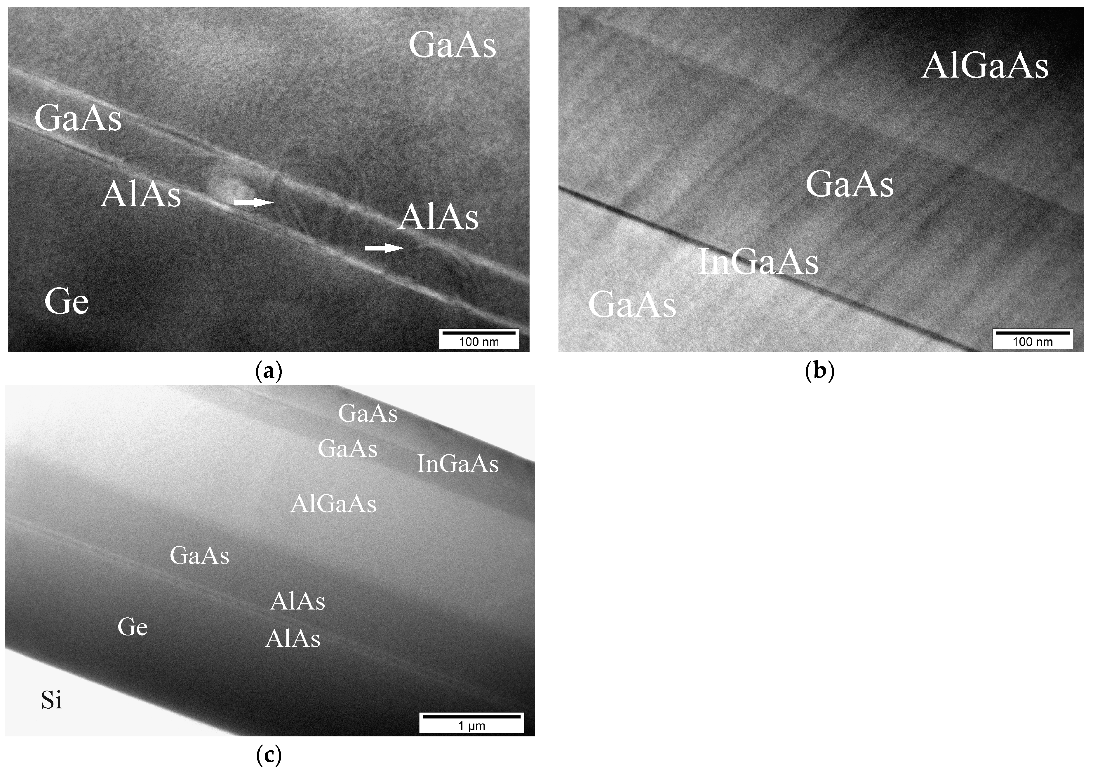
3. Growth of the A3B5 Nucleation Layer

At first we varied the growth regimes of the A3B5 nucleation layer. For the sample A grown on a “virtual” substrate # 1, the 100 nm thick GaAs nucleation layer was grown at 450 °C. Then, the growth temperature was raised to 620 °C, at which a 0.5-μm thick GaAs buffer layer was grown. After that formation of the laser structure including 1 μm thick Al0.3Ga0.7As cladding layers and a GaAs waveguide (0.8 μm thick) with three 10 nm thick InGaAs QWs (indium content is 0.18) inside was carried out. For the sample B, which was also grown on the “virtual” substrate # 1, the nucleation layer consisted of the alternating layers of AlAs (10 nm)/GaAs (50 nm)/AlAs (10 nm) grown at a high temperature (670 °C) at 0.33 nm/s. The V/III ratio was close to 30 during growth of these layers. All subsequent layers were grown similarly to the sample A. Thin AlAs layer at the GaAs/Ge interface reduces the mutual diffusion of atoms due to the high Al-As binding energy as was demonstrated in [14] and so prevents Ge penetration into the GaAs.
Optical properties of the grown structures were studied using the PL spectroscopy. A cw laser diode with λ = 0.8 μm was used for the excitation and the power density was ~5 W/cm2 for cw pumping. The stimulated emission was excited by the parametric oscillator Spectra-Physics MOPO-SL (emission wavelength 0.8 μm, pulse duration 5 ns, repetition rate 10 Hz). To record the PL signal, an Acton 2300i lattice monochromator and a multichannel photodetector based on the InGaAs photodiode array (spectral range 0.6–2.2 μm) were used. All measurements were carried out at room temperature.
TEM studies have shown that in the sample A, in which the GaAs layer was grown directly on Ge buffer, the defects formed at the GaAs/Ge heterointerface (Figure 1a) have propagated through the entire structure up to the surface. At the same time, in the sample B, in which the growth of the A3B5 part of the structure began from the AlAs/GaAs/AlAs lattice, most of the defects have been trapped between the layers of AlAs and did not pass further (Figure 1b). As a result, subsequent layers and the active region with InGaAs/GaAs QWs contain much lower concentration of structural defects (Figure 1c). Moreover, according to the AFM data, the surface roughness of the GaAs layer grown with the AlAs inserts on such a Ge/Si virtual substrate is nearly 2 times lower than in the case of growth of the same structure but without the AlAs inserts.
Due to the nominally zero offcut of the Si(001) substrate, the AFM studies have revealed the formation of the APBs during growth of the A3B5 compounds (Figure 1d)). The V-groove shaped features seen as dark lines in the AFM image (marked by black arrows in Figure 1d) correspond to the APBs as was shown in [15] and [16]. The APB density (in μm−1) has been estimated as the total length of the APBs on a specified section of the sample surface to the area of this section. The APB density has been found to be about 0.6 μm−1 after the deposition of the GaAs buffer layer (AFM image in Figure 1d), i.e., before the growth of the active region of the structure. After the formation of the whole structure, the APB density has even decreased to the value of nearly 0.3 μm−1. These values of the APB density are significantly smaller than the typical ones obtained during growth of polar materials on the exactly oriented non-polar Si(001) substrates [16,17]. We believe that the influence of the APBs is not the main critical factor affecting the optical properties of the grown A3B5/Ge/Si(001) structure. In particular, it was shown recently that the APB density of 3.7 μm−1 leads to nearly 2.5 times decrease of the photoluminescence signal in GaAs/Si(001) layers compared to control structures without APBs [16]. Due to the fact that in our sample the APB density is nearly 6 times smaller it is supposed that the APBs are, at least, not the major factor influencing the radiative recombination of charge carriers in the grown structure.
Figure 2 shows the PL spectra of samples A and B under cw pumping. It can be seen from the figure that the width of the PL peaks for both structures is quite large, which is a sign of the strong QW nonuniformity. Comparison of the PL spectra of samples A and B indicates that introduction of the AlAs layers at the GaAs/Ge interface allows to increase the PL intensity from QWs noticeably. Insertion of these AlAs layers also affects the threshold power density (see Figure 3). The threshold power densities were 45 kW/cm2 [18] and 75 kW/cm2 [19] for the samples B and A, respectively. The structure C which was grown similarly to the structure B (with the only one difference in the additional doping of the Al0.3Ga0.7As cladding layers provided in order to create a p-n junction), was used to fabricate the microstrip [20] and microdisk [21] laser diodes. At room temperature, diodes emitted at 0.99 μm (Figure 4) with a threshold current density of 5.5 kA/cm2 (pulse duration of 1 μs and repetition rate of 400 Hz) for a 2.7 mm long and 20 μm microstrip laser and 28 kA/cm2 (pulse duration of 0.5 μs and repetition rate of 150 Hz) for the 27 μm diameter microdisk laser. Increase of the threshold current density in the case of a microdisk laser is associated with the increase of the nonradiative recombination rate at the microdisk sidewalls due to the absence of any passivation.

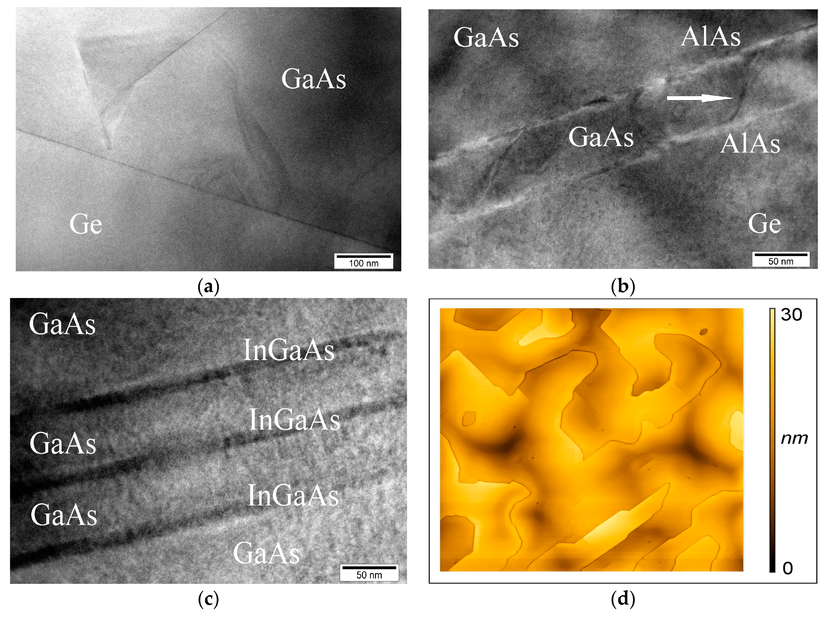
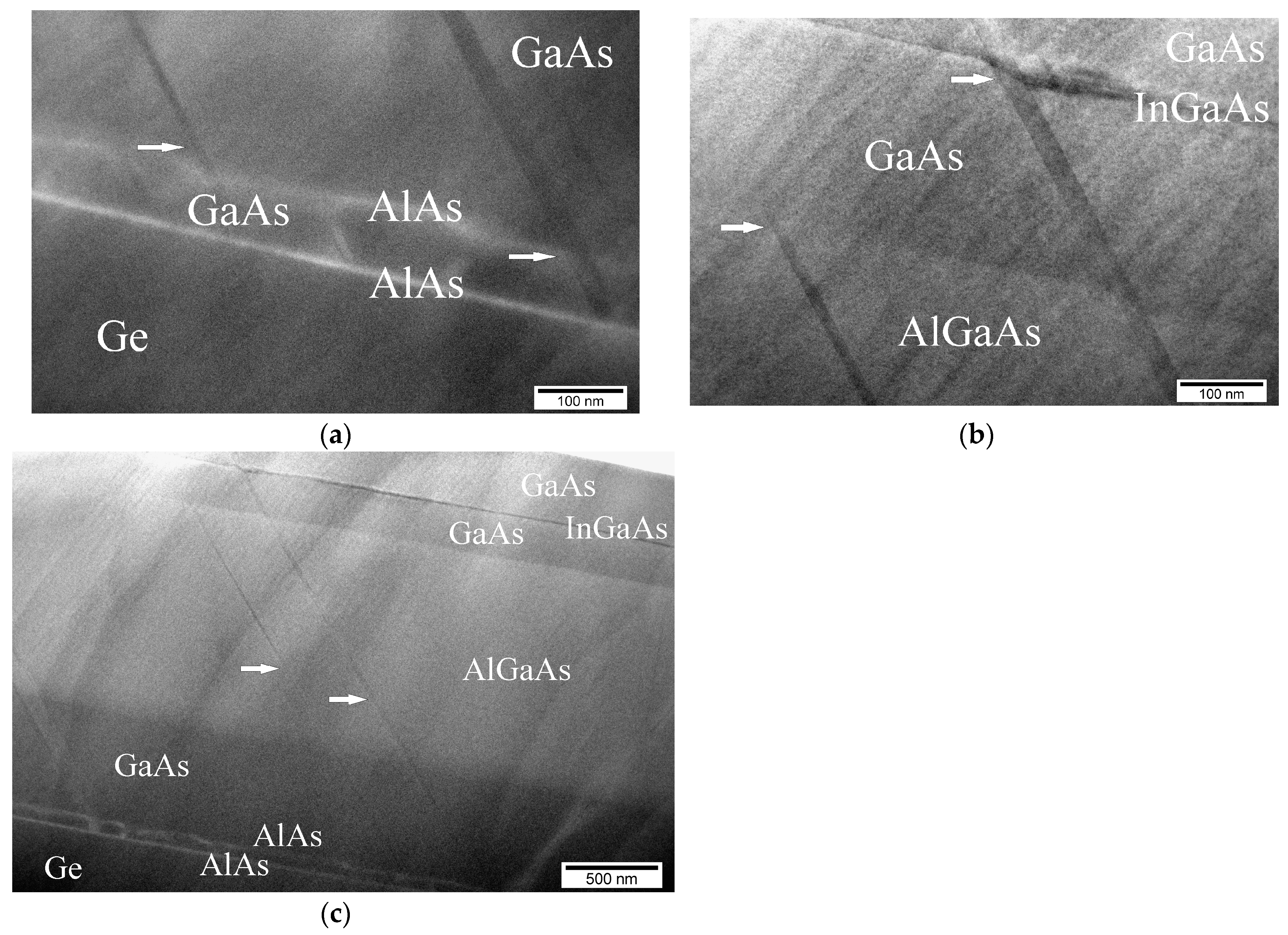
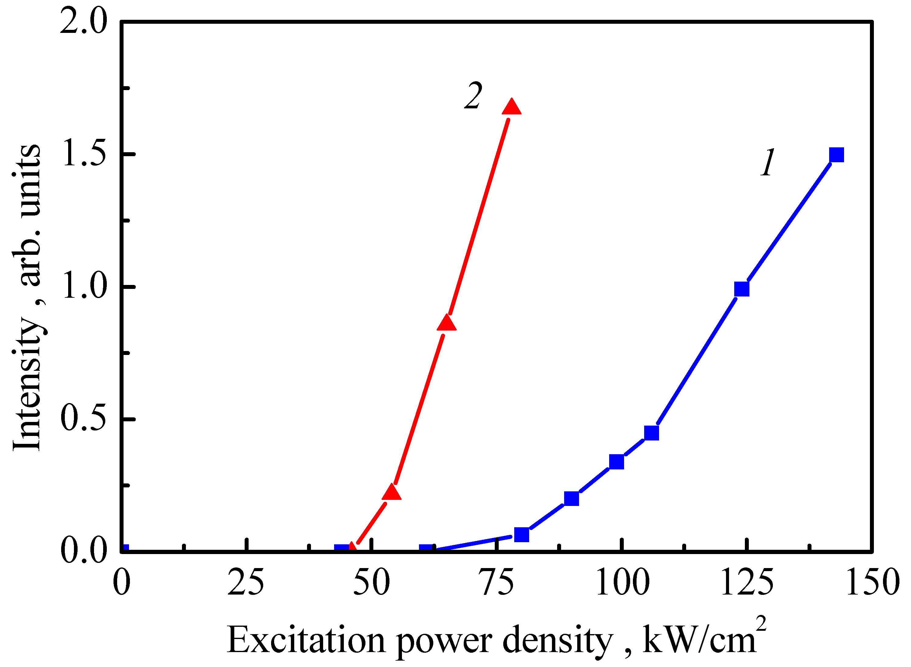
4. Growth of A3B5 Laser Structures on Ge/Si Substrates with Various Ge Layer Thicknesses

As was shown in the previous section, the use of the AlAs(10 nm)/GaAs(50 nm)/AlAs(10 nm) nucleation layer allows to significantly improve the structural and optical quality of the A3B5 laser structures fabricated on a Ge/Si “virtual” substrate. Therefore, all the structures described below were grown using this type of nucleation layer. In this section, the influence of the Ge layer thickness on the crystalline and optical quality of the A3B5 structures is described. In order to do this the samples D (using the substrate # 1) and E (using the substrate # 2) were simultaneously grown in the reactor. These samples differed from the sample B by the active region—only one InGaAs QW with high in content of 0.4 and the thickness of 5 nm was grown at 600 °C. Such a heavily strained InGaAs QW had the thickness close to the critical one for pseudomorphic growth.
An increase of the In fraction in the QW from 0.18 to 0.4 made it possible to obtain a PL signal with a sufficiently high intensity at a wavelengths longer than 1.1 μm (Figure 5). This indicates the possibility of creating a hybrid A3B5 QW-based laser on the exact Ge/Si substrate operating in the Si transparency window. Figure 5 shows the spectra of the stimulated emission of laser structures D and E, differing only by the thickness of Ge buffer layer under the optical excitation. Note that although samples D and E were grown in the same growth cycle, the stimulated emission wavelength of the sample with “thin” Ge layer was 1.123 μm while it was 1.11 μm for the sample with “thick” Ge layer. In spite of rather small difference between the PL intensities of the samples D and E, a significant (by a factor of 6) difference in the threshold power density was observed (see Figure 6). Indeed, the threshold power densities were 10 and 60 kW/cm2 for the samples D and E, respectively [22].
Increase of the threshold power density with the decrease of the Ge layer thickness can be explained by the increase of the defect density in the active region, which enhances the nonradiative recombination rate. Probably the higher defect density in the sample E results in higher QW thickness inhomogeneity leading to the observed red shift of the emission as compared to the sample D.
The structure F created on the basis of the structure D, differing only by the additional doping of the Al0.3Ga0.7As cladding layers (needed to create a p-n junction), was used to fabricate a strip laser diode [23]. A 1 mm long and a 15 μm wide laser diode emitted light in the wavelength range of 1.1 μm with a threshold current density of 20 kA/cm2 under electrical pumping (pulse duration of 0.36 μs and repetition rate of 1470 Hz) at room temperature (Figure 7).

5. InGaAs/GaAs/AlGaAs Laser Structures Grown by MOCVD on the Exact and Offcut Ge/Si(001) Substrates

In almost all cases reported in literature, the growth of A3B5 laser structures was carried out on 4°–6° offcut Si(001) substrates in order to avoid the formation of the antiphase boundaries (APB) which occur in the case of deposition of the polar material on a nonpolar substrate [24]. However, the existing Si-based technology is developed for the nominal Si(001) substrates (with the offcut angle smaller than 0.5°) [4], which complicates the employment of the offcut substrates. Therefore, usage of the exactly oriented Si(001) substrates is preferable for the integration of the active A3B5 elements with silicon microelectronics platform.
In order to compare the radiative characteristics under optical pumping, the laser structures were grown both on the exact and 4 degrees offcut Si(001) substrates.
Growth of the laser heterostructures G and H was carried out on the exact (“virtual” substrate # 1) and the offcut (“virtual” substrate # 4) Ge/Si substrates, respectively, in the AIX 200RF MOCVD reactor at reduced pressure (100 mbar). The structures were grown using an AlAs/GaAs/AlAs nucleation layer which was described above.
After the AlAs/GaAs/AlAs nucleation layer, a GaAs layer with a thickness of 500 nm and a AlGaAs cladding layer were grown at a temperature of 720 °C. The layers surrounding the InGaAs QW layers were grown at 620 °C. The V/III ratio was 80. Thin (20 nm) AlGaAs layer was deposited on top of the structure to reduce the influence of surface recombination and further capped by a thin GaAs layer to prevent its oxidation. The detailed parameters of the laser structures are given in the Table 2.
TEM studies have shown that in the sample G grown on the exact substrate, most of the defects are trapped between the AlAs layers and do not propagate further (Figure 8a). As a result, subsequent layers and the active region with InGaAs QW contain a much lower concentration of structural defects (Figure 8b,c).
At the same time, in the sample H which was grown on the offcut substrate, the AlAs/GaAs/AlAs nucleation layer prevents the formation of defects much weaker (Figure 9a), and they propagate through the entire structure up to the surface (Figure 9b,c). The substrate offcut led to the significant inhomogeneity of the AlAs second layer which further affected the optical properties of the structure.
Figure 10 shows the stimulated emission spectra of structures G and H. It can be seen from the figure that, despite the fact that A3B5 parts of the structures were grown simultaneously, the positions of the stimulated emission peaks are significantly different. This difference is probably due to the dependence of the in insertion in the InGaAs quantum well on the substrate offcut. Another reason is the inferior quality of the InGaAs QWs in the structure grown on the offcut substrate, as was shown by TEM.
In structure H, the wavelength of the stimulated emission is ~1.11 μm while in the structure G this wavelength is greater than 1.13 μm. We note that in both cases, the emission wavelength lies in the transparency region of bulk silicon, which makes these light sources suitable for low-loss silicon waveguides.
Figure 11 shows the dependences of the integral intensity of stimulated emission for the structures G and H on the excitation power density. The threshold power densities were calculated to be ~37 kW/cm2 for the structure grown on the offcut substrate and ~45 kW/cm2 for the structure grown on the exact substrate. Although the threshold for the structure H was slightly lower than for the structure G, the emission intensity of the structure G was remarkably higher than that of the structure H above the threshold, which indicates higher quantum efficiency of the structure fabricated on the exact substrate, and, consequently, its higher crystalline quality.

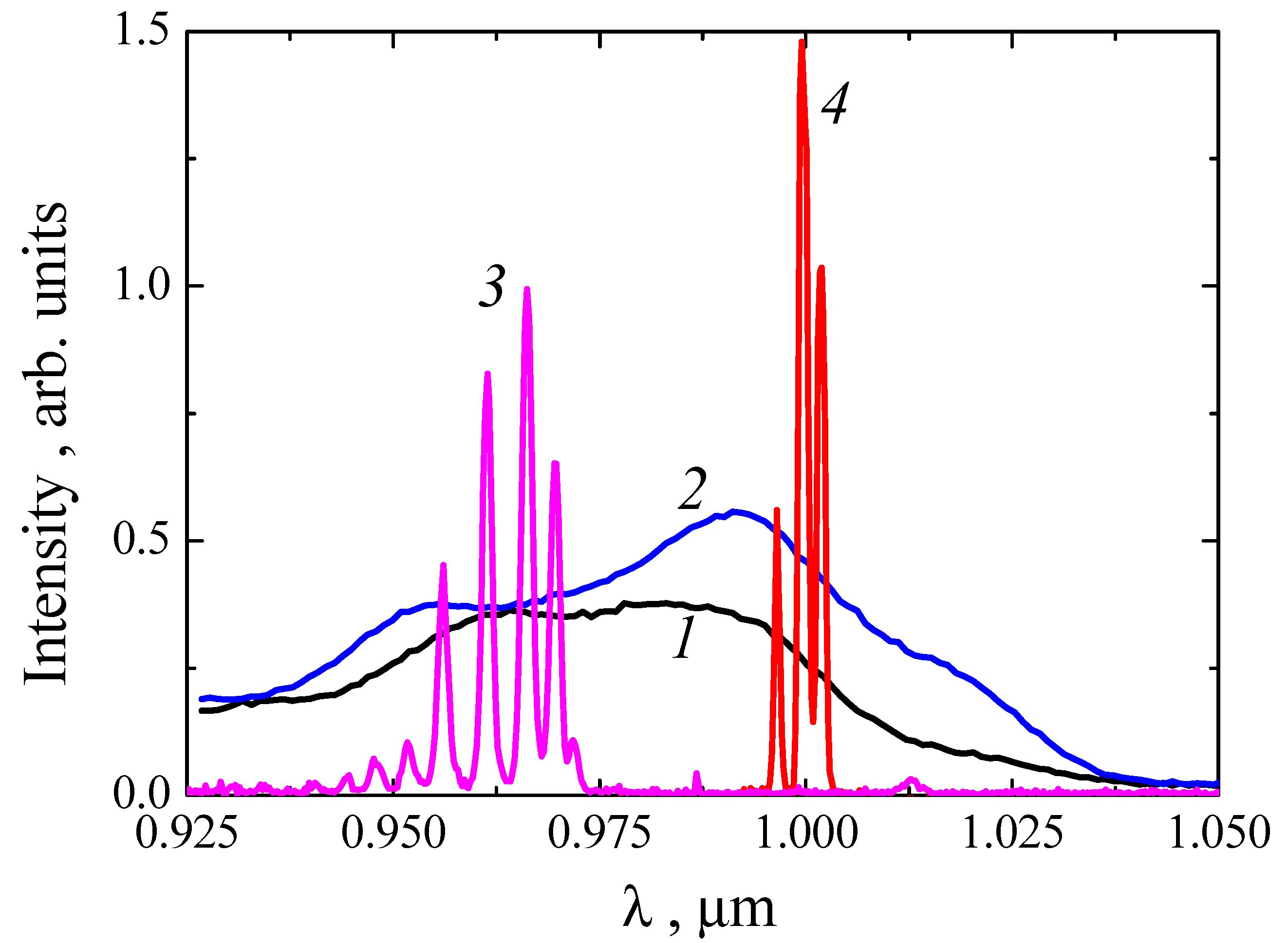
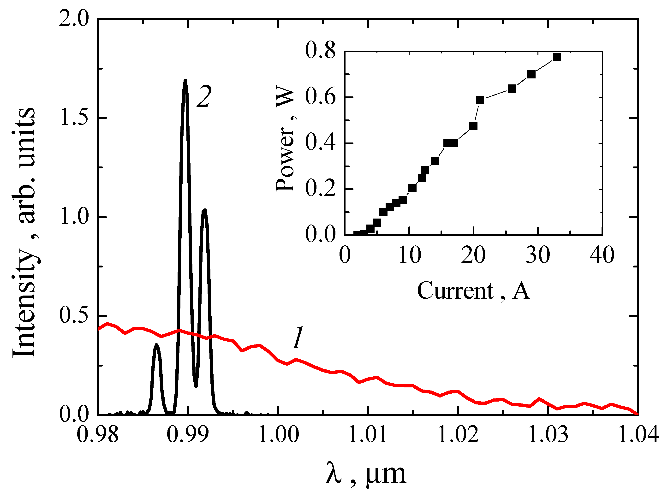
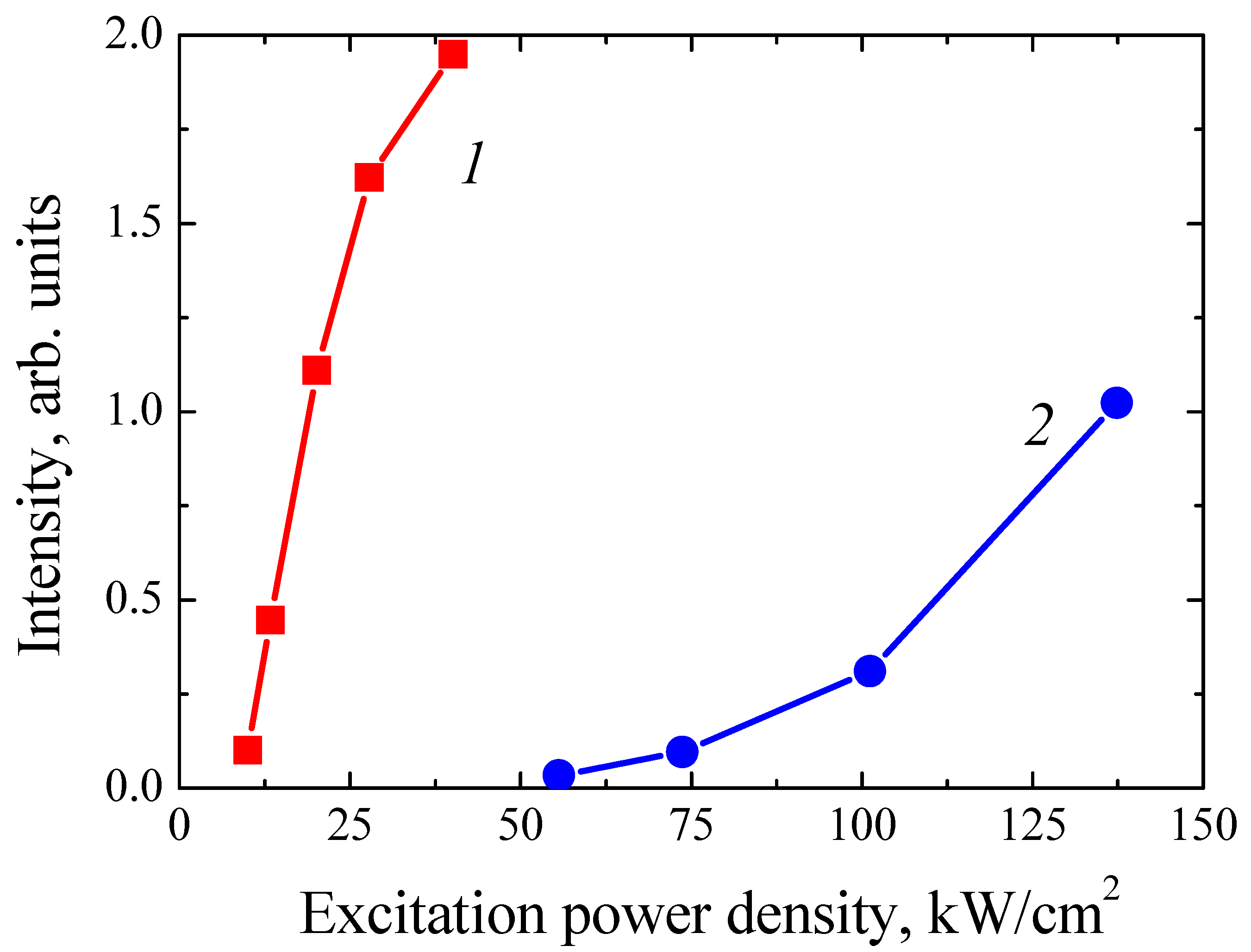
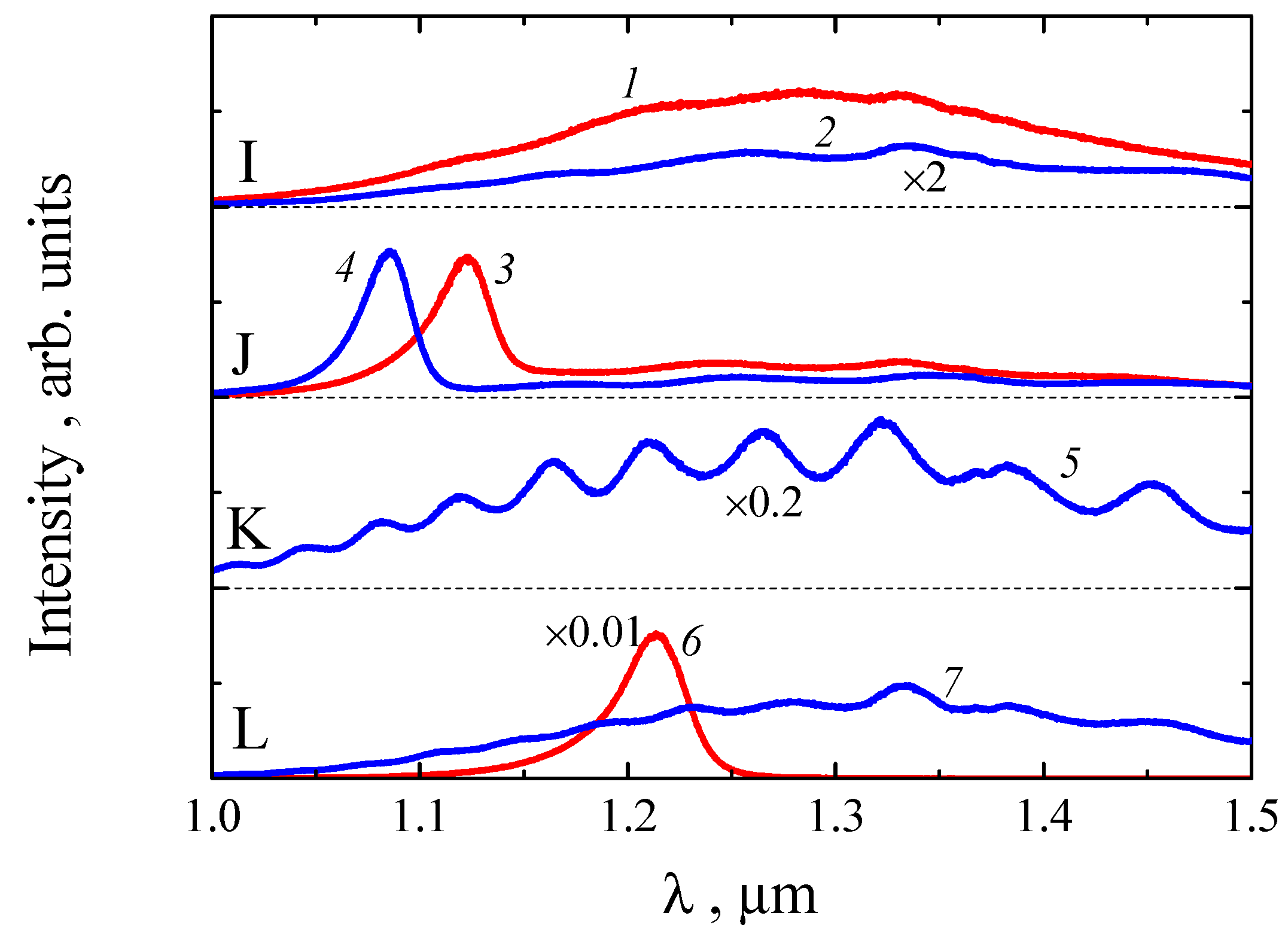
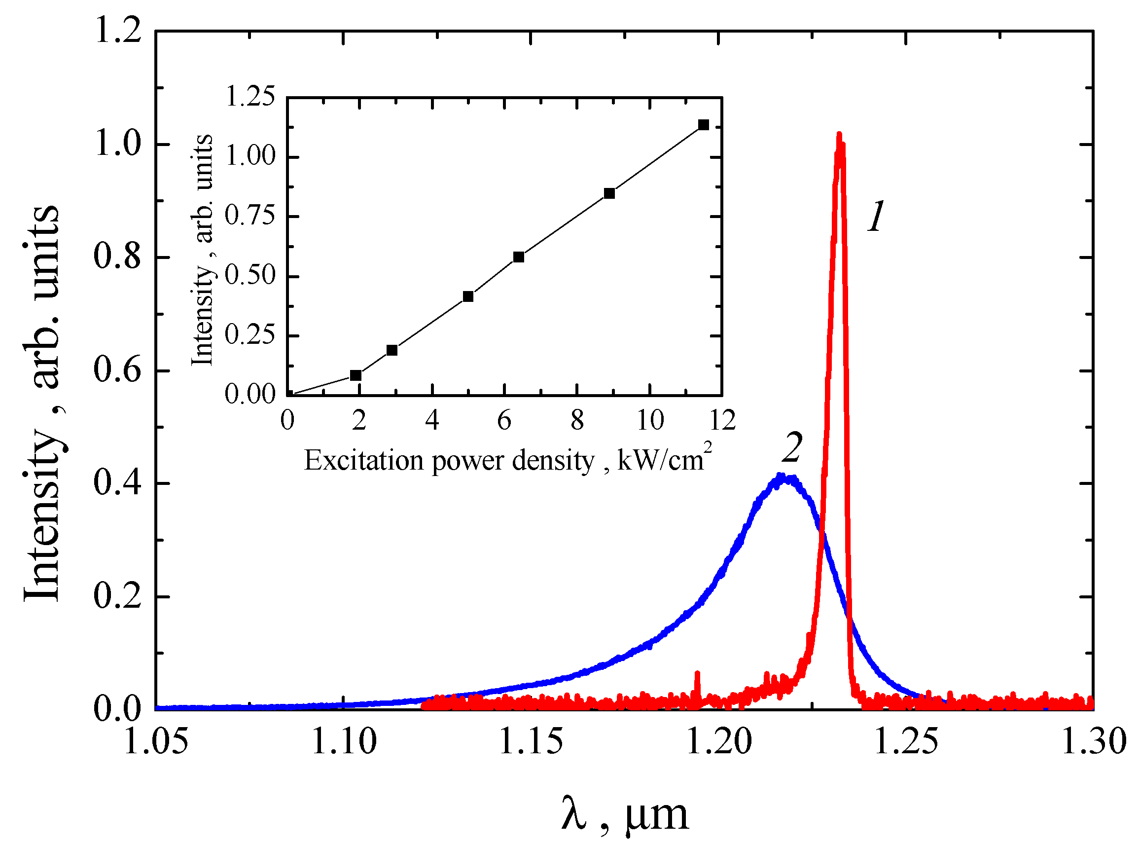
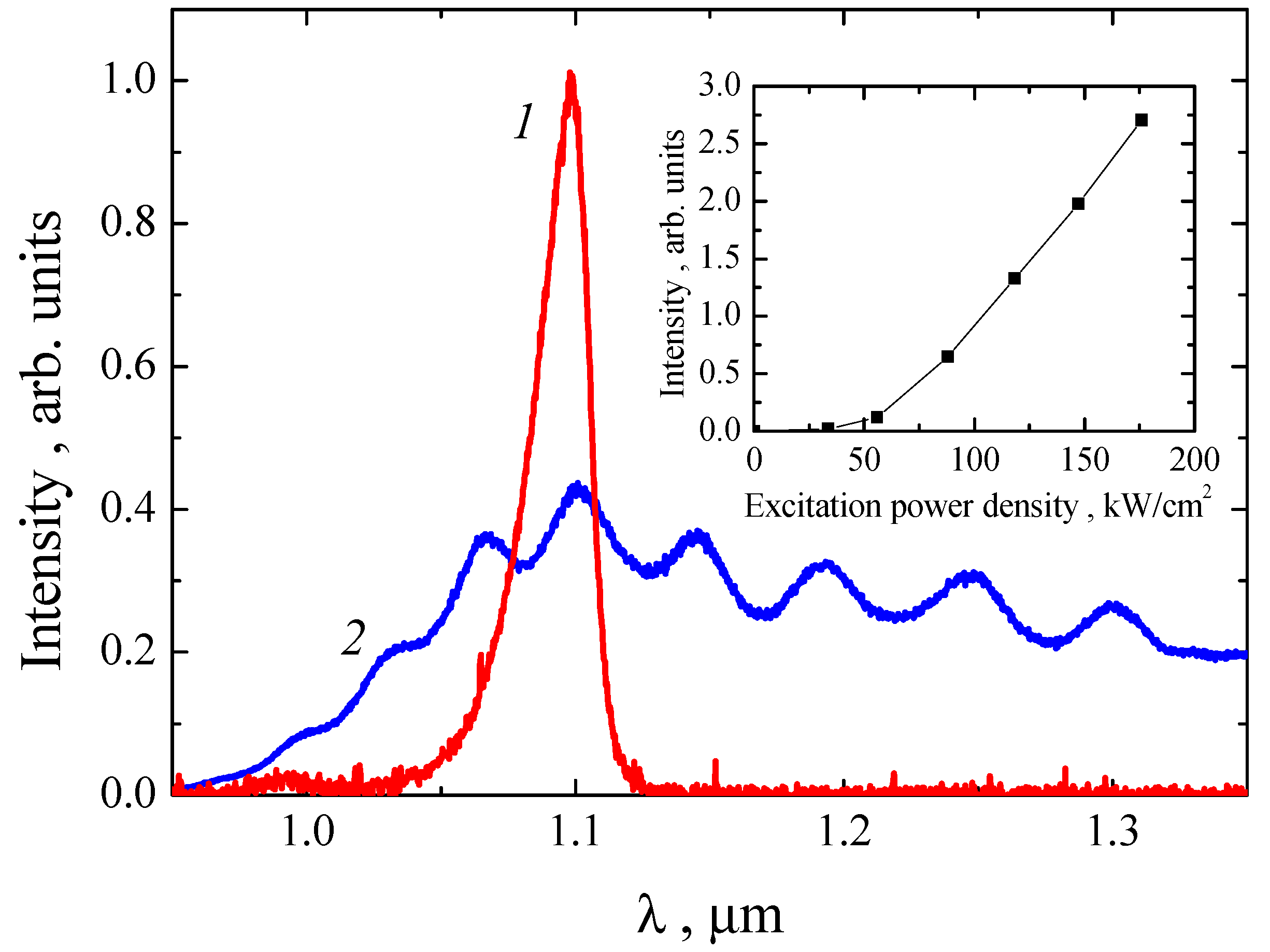
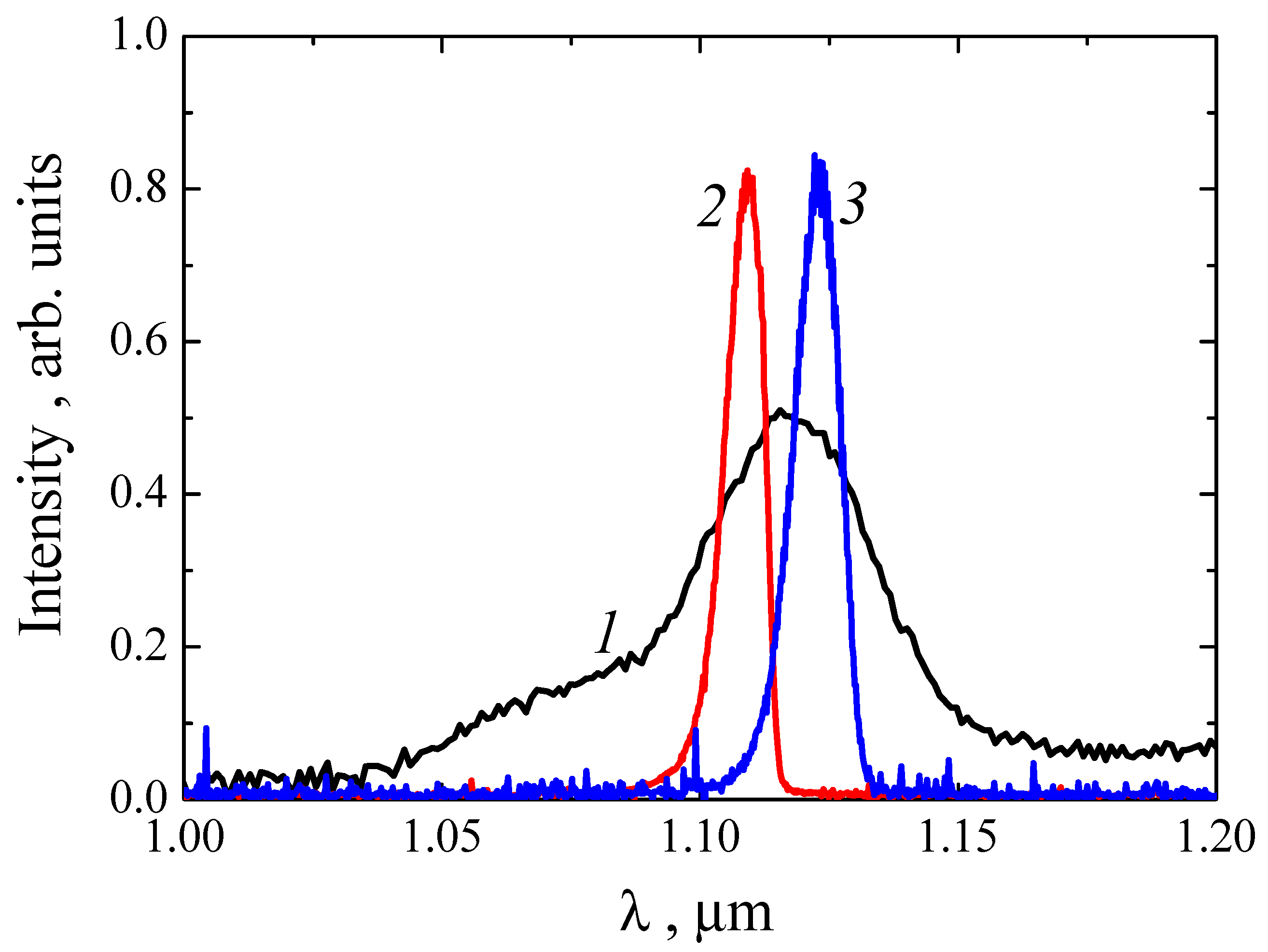
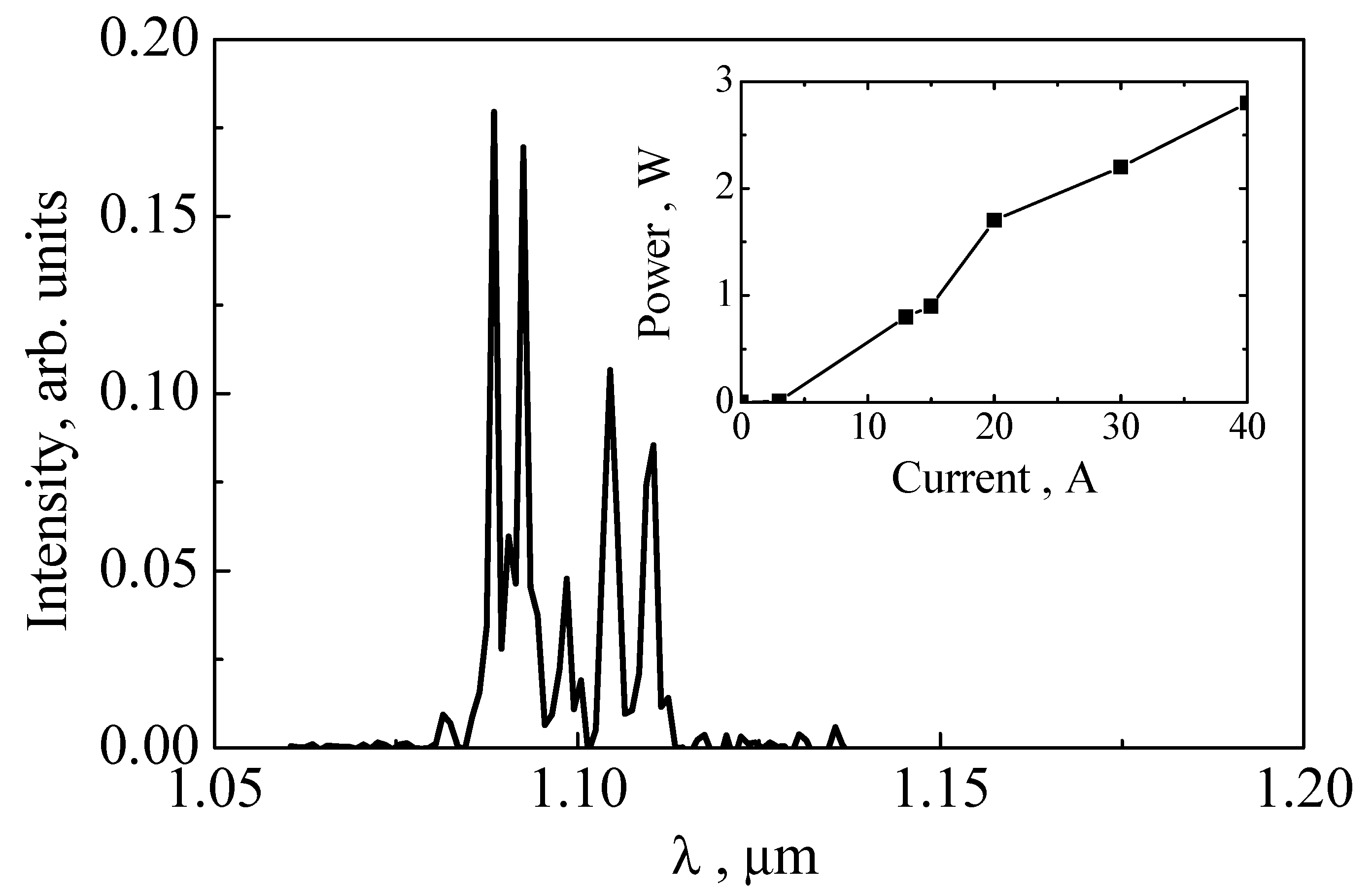
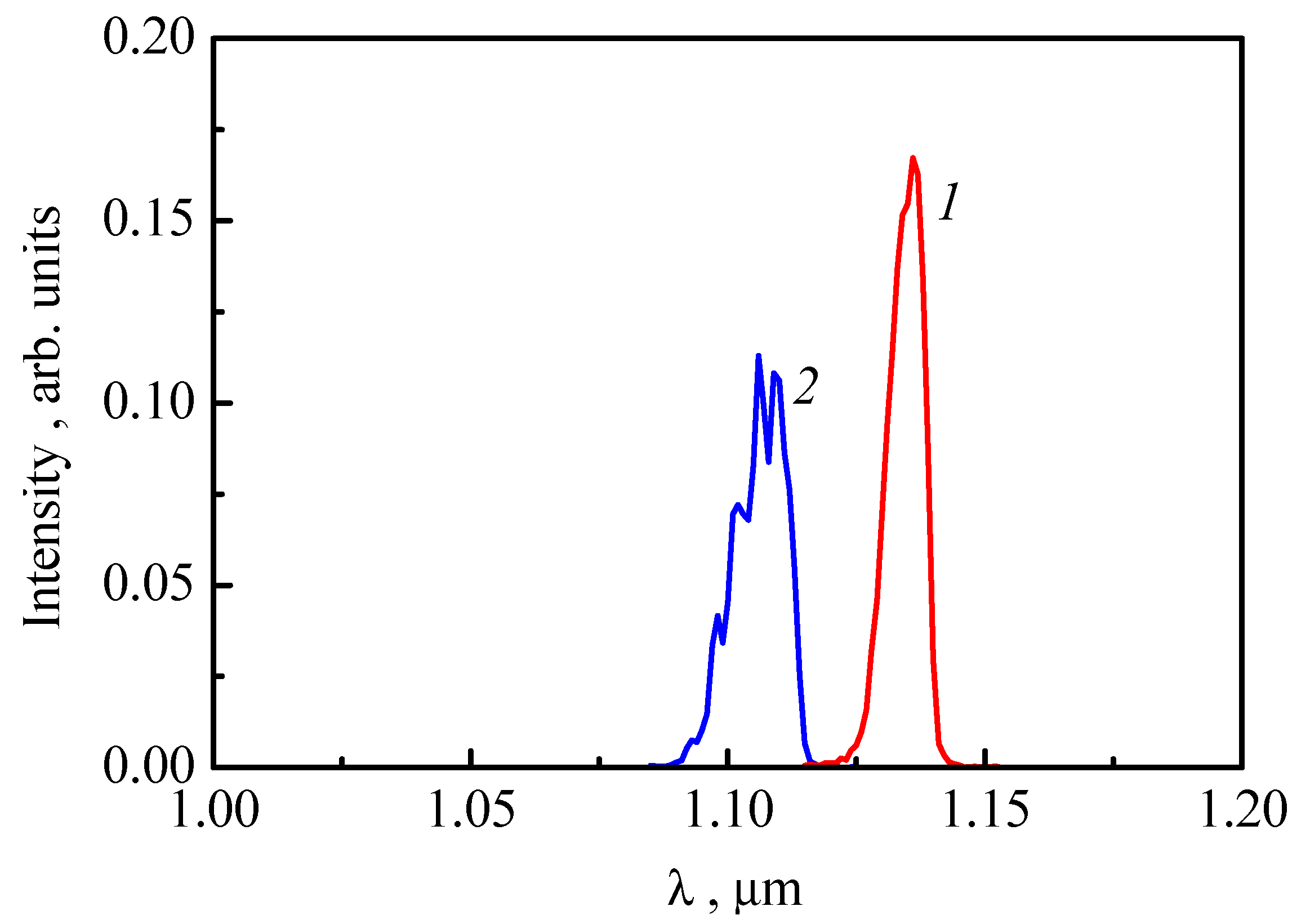
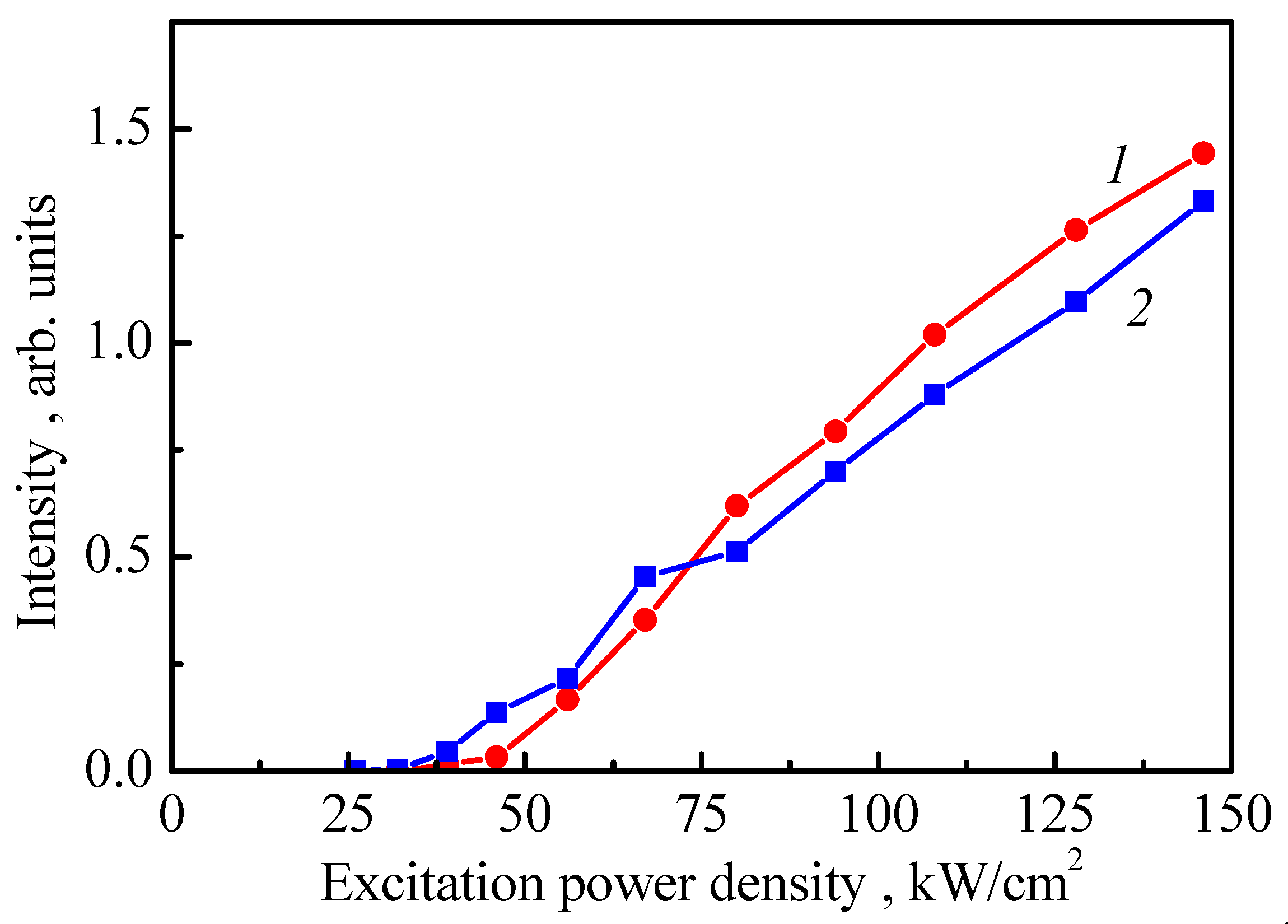
6. The Growth of Laser Heterostructures with InGaAs Quantum Wells Emitting at Wavelengths Longer Than 1.1 μm

For the growth of laser structures with strained InGaAs QWs and strain-compensating GaAsP layers, only the exact Ge/Si(001) virtual substrates with 1 μm thick Ge buffer were used. The laser structure formation began from the deposition of a buffer consisting of three periods of AlAs/GaAs (20/50 nm) to reduce the number of defects during the transition from Ge to GaAs. A thick (2 μm) GaAs buffer layer was then grown, containing 5 In0.15Ga0.85As/GaAs QWs with thickness of 10 nm each, which act as the dislocation filters. The Al0.3Ga0.7As layer with a thickness of 1 μm was deposited on such buffer and then the waveguide layer (250 nm of GaAs, the active region with InGaAs QWs with compensating GaAsP layers, and 350 nm of GaAs) and the capping layers (20 nm layer of Al0.3Ga0.7As to suppress the surface recombination and a 10 nm GaAs layer to prevent the structure oxidation) were deposited. In the series of laser structures, the In fraction in the InxGa1−xAs QWs (x = 0.38 ÷ 0.45) and the QWs width (6 ÷ 9 nm) were varied, as well as the parameters of the strain-compensating GaAs1−yPy layers (P fraction y = 0.1 ÷ 0.15, thickness d = 10 ÷ 15 nm) which were located on both sides of the QW and separated from it by a GaAs spacer layers of 2–10 nm thick. The parameters of some of the studied samples are listed in Table 3.
The active region of laser structures was grown at a lower temperature (530 ÷ 600 °C) to reduce the probability of strain relaxation. We note that the growth temperature is the most important parameter for the growth of QWs with thicknesses above the critical values. It is also necessary to take into account the strong effect of temperature on the composition of InGaAs and GaAsP. To obtain the high-quality GaAsP layers, additional studies were carried out aimed to determine the optimal growth temperatures of layers and the ratios of phosphine and arsine fluxes. Similar structures were also grown on GaAs substrates as references.
Figure 12 shows the RT PL spectra for a series of samples under study. The strain relaxation in the QW was observed for a sample I which did not contain strain-compensating GaAsP layers, even for the minimum values of the In fraction in the InGaAs QW and the minimum width of the QW (x ~0.39 and d ~ 7.5 nm, respectively). The characteristic width of the PL spectra (spectra (1), (2) in Figure 12) is hundreds of nanometers, and the PL intensity is comparable for the samples grown on GaAs and Ge/Si substrates. At the same time, as the PL spectra of subsequent samples show, the “insertion” of GaAsP layers allows to sufficiently suppress the relaxation of elastic strain in the QW with a noticeably larger fraction of In and greater QW thickness. In this case, one can see a pronounced peak with a width of 25–30 nm in the PL spectra (spectra (3), (4) in Figure 12) against a broad weak background which indicates a partial relaxation of the elastic strain.
For the QW parameters range in which it was possible to form the strained InGaAs QW on GaAs and Ge/Si substrates, the emission wavelength for the samples grown on Ge/Si substrates was noticeably (by 40–70 nm) shorter than for their reference counterparts grown on GaAs. This was associated with worse In embedding into the InGaAs QW in the case of growth on Ge/Si substrates. As the prerequisites for this one can consider the differences in surface morphologies of the samples grown on GaAs and Ge/Si substrates. First, the virtual Ge/Si substrates were initially significantly more defective (threading dislocation densities of 107 ÷ 108 cm−2 [11]) in comparison with GaAs substrates. Secondly, APBs appear during growth on Ge/Si substrates which lead to the formation of a developed surface with a roughness of at least several nanometers [20]. The high density of defects and the higher surface roughness can significantly affect the incorporation of in adatoms into the InGaAs QW.
Further, as the In fraction in the QW was increased, we observed the following. The proper selection of growth conditions made it possible to form nearly defect-free strained QWs with an In fraction up to x = 0.46 in the case of growth on GaAs substrates using the GaAsP strain-compensating layers. The fabricated samples demonstrated intense PL at the wavelengths of up to 1.22–1.24 μm with a characteristic peak width of 30–40 nm (spectrum (6) in Figure 12). Relaxation of the elastic strain via formation of misfit dislocations and subsequent strong degradation of the optical properties was observed for the similar parameters of QWs and strain-compensating layers in the case of growth on Ge/Si substrates. The maximum emission wavelength achieved using the Ge/Si substrates was 1.12–1.13 μm with a QW width of 8 nm and an In fraction of x = 0.4 (spectrum (4) in Figure 12). The faster onset of strain relaxation as compared with growth on GaAs substrates can be attributed to the much higher initial concentration of threading dislocations and the inevitable formation of the APBs.
Under conditions of strong pulsed pumping, a significant reduction of the QW emission linewidth and a typical threshold behavior were observed for a number of samples under study. This indicates the realization of the stimulated emission (SE) regime. For the structures grown on GaAs substrates, the longest wavelength of SE (1.24 μm) was obtained for the sample L (Figure 13). The SE threshold was ~1 kW/cm2 at room temperature. This result is close to the record values obtained earlier for strained InGaAs QW [25]. In the case of growth on Ge/Si substrates the SE was observed at T = 77 K (Figure 14). At the same time, the longest SE wavelength of only ~1.1 μm (structure K) was reached and a threshold was nearly 60 kW/cm2. Such a high threshold is mainly associated with the partial strain relaxation in the QW region in the case of growth on Ge/Si substrates despite the usage of strain-compensating layers contrary to the nearly full suppression of strain relaxation in the case of growth on GaAs.

7. Conclusions

In this paper we reported about the features of MOCVD growth of the GaAs/AlGaAs laser heterostructures with InGaAs QWs on the exact and 4° offcut Si(001) substrates with the Ge buffer layers of various thicknesses. Different growth regimes at the initial stages of A3B5 deposition were studied. It was demonstrated that the use of a buffer consisting of alternating layers of AlAs and GaAs leads to the significant decrease of the defect density in A3B5 laser structures grown on Ge/Si(001) substrates. In addition, it was shown that the decrease of Ge layer thickness from 1 μm to 0.3 μm leads to a degradation of the crystalline quality of the laser structure and hence to the significant increase of the stimulated emission threshold.
A significant difference in the properties of samples grown under identical conditions on GaAs and Ge/Si substrates was observed in the case of growth of structures with highly strained InGaAs/GaAs QWs and strain-compensating GaAsP layers. For such structures, there are differences in the critical thickness of dislocations formation and differences in the efficiency of In incorporation during QW growth, which complicate the achieving of long-wavelength (>1.1 μm) luminescence and stimulated emission in structures grown on Ge/Si substrates. In the structures formed on GaAs substrates, stimulated emission was observed at a wavelength of 1.24 μm under pulsed pumping conditions at room temperature. In the case of growth on Ge/Si substrates the stimulated emission was observed only at T = 77 K and at a much smaller wavelengths (~1.1 μm). InGaAs/GaAs/AlGaAs laser diodes with QWs grown by MOCVD on the exact Ge/Si(001) substrates were created. Such diodes has shown stimulated emission in the pulsed mode at room temperature in the spectral range of 0.99–1.11 μm and with a threshold current density in the range of 5.5–20 kA/cm2.
The conducted investigations have shown the possibility of creating the QW hybrid lasers on Ge/Si(001) substrates using the MOCVD technology. However, it should be noted that the characteristics of the obtained lasers are noticeably inferior as compared with lasers using the quantum dots as an active media which were grown on Si substrates by the MBE [6,26,27] and very recently by MOCVD [28].

Author Contributions

Conceptualization, Z.K, V.A. and A.D.; Methodology, M.S., S.N., A.P. and P.Y.; Investigation, N.B., K.K., A.N., D.P., A.S. and D.Y.; Writing-Original Draft Preparation, N.B., V.A., A.D and D.Y.; Writing-Review & Editing, A.N. and Z.K.

Funding

The work was supported by the Russian Science Foundation (project # 14-12-00644).

Conflicts of Interest

The authors declare no conflict of interest.

References

  1. Sun, C.; Wade, M.T.; Lee, Y.; Orcutt, J.S.; Alloatti, L.; Georgas, M.S.; Waterman, A.S.; Shainline, J.M.; Avizienis, R.R.; Lin, S. Single-chip microprocessor that communicates directly using light. Nature 2015, 528, 534. [Google Scholar] [CrossRef] [PubMed]
  2. Liu, A.Y.; Zhang, C.; Norman, J.; Snyder, A.; Lubyshev, D.; Fastenau, J.M.; Liu, A.W.; Gossard, A.C.; Bowers, J.E. High performance continuous wave 1.3 μm quantum dot lasers on silicon. Appl. Phys. Lett. 2014, 104, 041104. [Google Scholar] [CrossRef]
  3. Chen, S.; Li, W.; Wu, J.; Jiang, Q.; Tang, M.; Shutts, S.; Elliott, S.N.; Sobiesierski, A.; Seeds, A.J.; Ross, I. Electrically pumped continuous-wave III–V quantum dot lasers on silicon. Nat. Photonics 2016, 10, 307. [Google Scholar] [CrossRef]
  4. Volz, K.; Beyer, A.; Witte, W.; Ohlmann, J.; Németh, I.; Kunert, B.; Stolz, W. GaP-nucleation on exact Si (0 0 1) substrates for III/V device integration. J. Cryst. Growth 2011, 315, 37–47. [Google Scholar] [CrossRef]
  5. Huang, X.; Song, Y.; Masuda, T.; Jung, D.; Lee, M. InGaAs/GaAs quantum well lasers grown on exact GaP/Si (001). Electron. Lett. 2014, 50, 1226–1227. [Google Scholar] [CrossRef]
  6. Liu, A.Y.; Peters, J.; Huang, X.; Jung, D.; Norman, J.; Lee, M.L.; Gossard, A.C.; Bowers, J.E. Electrically pumped continuous-wave 1.3 μm quantum-dot lasers epitaxially grown on on-axis (001) GaP/Si. Opt. Lett. 2017, 42, 338–341. [Google Scholar] [CrossRef] [PubMed]
  7. Tansu, N.; Mawst, L.J. High-performance strain-compensated InGaAs-GaAsP-GaAs (/spl lambda/= 1.17 μm) quantum well diode lasers. IEEE Photonics Technol. Lett. 2001, 13, 179–181. [Google Scholar] [CrossRef]
  8. Tansu, N.; Yeh, J.-Y.; Mawst, L.J. Low-threshold 1317-nm InGaAsN quantum-well lasers with GaAsN barriers. Appl. Phys. Lett. 2003, 83, 2512–2514. [Google Scholar] [CrossRef]
  9. Colace, L.; Masini, G.; Galluzzi, F.; Assanto, G.; Capellini, G.; Di Gaspare, L.; Palange, E.; Evangelisti, F. Metal–semiconductor–metal near-infrared light detector based on epitaxial Ge/Si. Appl. Phys. Lett. 1998, 72, 3175–3177. [Google Scholar] [CrossRef]
  10. Luan, H.-C.; Lim, D.R.; Lee, K.K.; Chen, K.M.; Sandland, J.G.; Wada, K.; Kimerling, L.C. High-quality Ge epilayers on Si with low threading-dislocation densities. Appl. Phys. Lett. 1999, 75, 2909–2911. [Google Scholar] [CrossRef]
  11. Yurasov, D.; Bobrov, A.; Daniltsev, V.; Novikov, A.; Pavlov, D.; Skorokhodov, E.; Shaleev, M.; Yunin, P. Impact of growth and annealing conditions on the parameters of Ge/Si (001) relaxed layers grown by molecular beam epitaxy. Semiconductors 2015, 49, 1415–1420. [Google Scholar] [CrossRef]
  12. Volkov, P.; Goryunov, A.; Luk’yanov, A.Y.; Tertyshnik, A.; Novikov, A.; Yurasov, D.; Baidakova, N.; Mikhailov, N.; Remesnik, V.; Kuzmin, V. Optical monitoring of technological parameters during molecular-beam epitaxy. Semiconductors 2012, 46, 1471–1475. [Google Scholar] [CrossRef]
  13. Souriau, L.; Atanasova, T.; Terzieva, V.; Moussa, A.; Caymax, M.; Loo, R.; Meuris, M.; Vandervorst, W. Characterization of threading dislocations in thin germanium layers by defect etching: Toward chromium and HF-free solution. J. Electrochem. Soc. 2008, 155, H677–H681. [Google Scholar] [CrossRef]
  14. Chia, C.; Dong, J.; Chi, D.; Sridhara, A.; Wong, A.; Suryana, M.; Dalapati, G.; Chua, S.; Lee, S. Effects of AlAs interfacial layer on material and optical properties of Ga As/Ge (100) epitaxy. Appl. Phys. Lett. 2008, 92, 141905. [Google Scholar] [CrossRef]
  15. Németh, I.; Kunert, B.; Stolz, W.; Volz, K. Heteroepitaxy of GaP on Si: Correlation of morphology, anti-phase-domain structure and MOVPE growth conditions. J. Cryst. Growth 2008, 310, 1595–1601. [Google Scholar] [CrossRef]
  16. Alcotte, R.; Martin, M.; Moeyaert, J.; Cipro, R.; David, S.; Bassani, F.; Ducroquet, F.; Bogumilowicz, Y.; Sanchez, E.; Ye, Z. Epitaxial growth of antiphase boundary free GaAs layer on 300 mm Si (001) substrate by metalorganic chemical vapour deposition with high mobility. Appl. Mater. 2016, 4, 046101. [Google Scholar] [CrossRef]
  17. Chriqui, Y.; Largeau, L.; Patriarche, G.; Saint-Girons, G.; Bouchoule, S.; Sagnes, I.; Bensahel, D.; Campidelli, Y.; Kermarrec, O. Direct growth of GaAs-based structures on exactly (0 0 1)-oriented Ge/Si virtual substrates: reduction of the structural defect density and observation of electroluminescence at room temperature under CW electrical injection. J. Cryst. Growth 2004, 265, 53–59. [Google Scholar] [CrossRef]
  18. Aleshkin, V.Y.; Baidus, N.; Dubinov, A.; Krasilnik, Z.; Nekorkin, S.; Novikov, A.; Rykov, A.; Yurasov, D.; Yablonskiy, A. On the stimulated emission of InGaAs/GaAs/AlGaAs laser structures grown by MOCVD on exact and inclined Ge/Si (001) substrates. Semiconductors 2017, 51, 663–666. [Google Scholar] [CrossRef]
  19. Aleshkin, V.Y.; Dikareva, N.; Dubinov, A.; Denisov, S.; Krasil’nik, Z.; Kudryavtsev, K.; Matveev, S.; Nekorkin, S.; Shengurov, V. Stimulated emission from an InGaAs/GaAs/AlGaAs heterostructure grown on a Si substrate. JETP Lett. 2015, 100, 795–797. [Google Scholar] [CrossRef]
  20. Aleshkin, V.Y.; Baidus, N.; Dubinov, A.; Fefelov, A.; Krasilnik, Z.; Kudryavtsev, K.; Nekorkin, S.; Novikov, A.; Pavlov, D.; Samartsev, I. Monolithically integrated InGaAs/GaAs/AlGaAs quantum well laser grown by MOCVD on exact Ge/Si (001) substrate. Appl. Phys. Lett. 2016, 109, 061111. [Google Scholar] [CrossRef]
  21. Kryzhanovskaya, N.; Moiseev, E.; Polubavkina, Y.S.; Maximov, M.; Kulagina, M.; Troshkov, S.; Zadiranov, Y.M.; Lipovskii, A.; Baidus, N.; Dubinov, A. Electrically pumped InGaAs/GaAs quantum well microdisk lasers directly grown on Si (100) with Ge/GaAs buffer. Opt. Express 2017, 25, 16754–16760. [Google Scholar] [CrossRef] [PubMed]
  22. Baidus, N.; Aleshkin, V.Y.; Dubinov, A.; Kudryavtsev, K.; Nekorkin, S.; Novikov, A.; Pavlov, D.; Rykov, A.; Sushkov, A.; Shaleev, M. Peculiarities of growing InGaAs/GaAs/AlGaAs laser structures by MOCVD on Ge/Si substrates. Semiconductor 2017, 51, 1527–1530. [Google Scholar] [CrossRef]
  23. Aleshkin, V.Y.; Baidus, N.; Dubinov, A.; Kudryavtsev, K.; Nekorkin, S.; Novikov, A.; Rykov, A.; Samartsev, I.; Fefelov, A.; Yurasov, D. Technology of the production of laser diodes based on GaAs/InGaAs/AlGaAs structures grown on a Ge/Si substrate. Semiconductor 2017, 51, 1477–1480. [Google Scholar] [CrossRef]
  24. Kroemer, H.; Polasko, K.J.; Wright, S.C. On the (110) orientation as the preferred orientation for the molecular beam epitaxial growth of GaAs on Ge, GaP on Si, and similar zincblende-on-diamond systems. Appl. Phys. Lett. 1980, 36, 763–765. [Google Scholar] [CrossRef]
  25. Sung, L.; Lin, H. Highly strained 1.24-μm InGaAs/GaAs quantum-well lasers. Appl. Phys. Lett. 2003, 83, 1107–1109. [Google Scholar] [CrossRef]
  26. Jung, D.; Norman, J.; Kennedy, M.; Shang, C.; Shin, B.; Wan, Y.; Gossard, A.C.; Bowers, J.E. High efficiency low threshold current 1.3 μ m InAs quantum dot lasers on on-axis (001) GaP/Si. Appl. Phys. Lett. 2017, 111, 122107. [Google Scholar] [CrossRef]
  27. Wan, Y.; Norman, J.; Li, Q.; Kennedy, M.; Liang, D.; Zhang, C.; Huang, D.; Zhang, Z.; Liu, A.Y.; Torres, A. 1.3 μm submilliamp threshold quantum dot micro-lasers on Si. Optica 2017, 4, 940–944. [Google Scholar] [CrossRef]
  28. Wang, J.; Hu, H.; Yin, H.; Bai, Y.; Li, J.; Wei, X.; Liu, Y.; Huang, Y.; Ren, X.; Liu, H. 1.3 μm InAs/GaAs quantum dot lasers on silicon with GaInP upper cladding layers. Photonics Res. 2018, 6, 321–325. [Google Scholar] [CrossRef]
Figure 1. TEM images of the cross section of InGaAs/GaAs/AlGaAs laser heterostructures grown on the Ge/Si substrate: (a) GaAs/Ge heterointerface for the sample A, (b) the same heterointerface with the AlAs/GaAs/AlAs insertions for the sample B, (c) active region with three InGaAs/GaAs QWs of the sample B, (d) AFM image of the GaAs layer grown on this Ge/Si virtual substrate with the AlAs/GaAs/AlAs insertions between the main GaAs buffer layer and Ge. Scan sizes are 13 × 13 μm2.
Crystals 08 00311 g001
Figure 2. PL spectra of the samples A (1) and B (2) under cw pumping and also stimulated emission spectra of the samples A (3) and B (4).
Crystals 08 00311 g002
Figure 3. Dependence of the emission intensity of the optically pumped laser structures on the excitation power density for the samples A (1) and B (2).
Crystals 08 00311 g003
Figure 4. The emission spectrum at room temperature of a microstrip laser made from the structure C at a current of 2 A (current density of 3.7 kA/cm2) (1) and a current of 14 A (current density of 26 kA/cm2) (2). The inset shows the power-current characteristic of this microstrip laser.
Crystals 08 00311 g004
Figure 5. The PL spectra of the sample D (curve 1) and the stimulated emission spectra of the samples D (curve 2) and E (curve 3).
Crystals 08 00311 g005
Figure 6. Dependences of the emission intensity of laser structures under the optical pumping on the excitation power density for the structures D (curve 1) and E (curve 2).
Crystals 08 00311 g006
Figure 7. The emission spectrum of a strip laser based on the structure F at a current of 40 A (current density of 265 kA/cm2). The inset shows the power-current characteristic of this laser.
Crystals 08 00311 g007
Figure 8. TEM images of the cross section of the laser heterostructure G: (a) Heterointerface with AlAs/GaAs/AlAs layers, (b) active region with InGaAs/GaAs QWs, (c) cross-section of the entire heterostructure. The white arrows indicate defects.
Crystals 08 00311 g008
Figure 9. TEM images of the cross section of the laser heterostructure H: (a) Heterointerface with AlAs/GaAs/AlAs layers, (b) active region with InGaAs/GaAs QWs, (c) cross section of the entire heterostructure. The white arrows indicate defects.
Crystals 08 00311 g009
Figure 10. Stimulated emission spectra from the structures G (1) and H (2).
Crystals 08 00311 g010
Figure 11. Dependencies of the integral intensity of stimulated emission in the structures G (1) and H (2).
Crystals 08 00311 g011
Figure 12. PL spectra of the structures I, J, K, L (see Table 3) with InGaAs/GaAs QWs grown on GaAs (1, 3, 6) and Ge/Si substrates (2, 4, 5, 7). Oscillations in the PL spectra of structures grown on Ge/Si substrates are due to the interference effects.
Crystals 08 00311 g012
Figure 13. Spectrum of stimulated emission of the structure with the strained In0.46Ga0.54As/GaAs QW grown on a GaAs substrate (1). For comparison, the spectrum of spontaneous emission is shown (not to scale) (2). The pumping power densities are 5 kW/cm2 and 5 W/cm2 for (1) and (2), respectively. The measurement temperature is T = 300 K. Dependence of the integral emission intensity on the excitation power density is shown in the inset.
Crystals 08 00311 g013
Figure 14. Spectrum of stimulated emission of the structure with the strained In0.43Ga0.57As/GaAs QW grown on a Ge/Si substrate (1). For comparison, the spectrum of spontaneous emission is shown (not to scale) (2). The pumping power densities are 100 kW/cm2 and 5 W/cm2 for (1) and (2), respectively. The measurement temperature is T = 77 K. Dependence of the integral emission intensity on the excitation power density is shown in the inset.
Crystals 08 00311 g014
Table 1. Parameters of Ge/Si (001) virtual substrates.
Substrate NumberOffcut AngleGe Layer ThicknessRMS Roughness
(Scan Area 13 × 13 μm)
Ge(004) Rocking Curve WidthDensity of Threading Dislocations
1<0.5°1 µm1 nm0.059°~107 cm−2
2<0.5°0.3 µm1.3 nm0.1°(5–7)·108 cm−2
3<0.5°0.5 µm1.3 nm0.066°(6–8)·107 cm2
41 µm1 nm0.059°~107 cm−2
Table 2. Parameters of laser structures G and H.
Layer NumberLayer CompositionLayer Thickness, nm
1AlAs10
2GaAs50
3AlAs10
4GaAs500
5gradient GaAs-Al0.3Ga0.7As100
6Al0.3Ga0.7As1000
7GaAs250
8InxGa1−xAs10
9GaAs350
10Al0.3Ga0.7As20
11gradient Al0.3Ga0.7As-GaAs10
12GaAs10
Table 3. Characteristics of samples with heavily strained InGaAs QWs and GaAsP Strain-compensating layers. Sample name (capital letter), In fraction in the QW (x[In]), QW thickness (dQW), P fraction in the strain-compensating layers (x[P]) and their thickness (dCL), as well as the growth temperature (Tgr) are indicated in the corresponding columns.
x[In]dQW, nmx[P]dCL, nmTgr, °C
I0.397.5--600
J0.480.1110600
K0.437.50.1412530
L0.4490.12515530

