Abstract
Organic-inorganic hybrid perovskite has attracted intensive attention from researchers as the gain medium in lasing devices. However, achieving electrically driven lasing remains a significant challenge. Modifying the devices’ structure to enhance the optically pumped amplified spontaneous emission (ASE) is the key issue. In this work, gold nanoparticles (Au NPs) are first doped into PEDOT: PSS buffer layer in a slab waveguide device structure: Quartz/PEDOT: PSS (with or w/o Au NPs)/CH3NH3PbBr3. As a result, the facile device shows a significantly enhanced ASE intensity and a narrowed full width at half maximum. Based on experiments and theoretical simulation data, the improvement is mainly a result of the compound surface plasmon resonance, including simultaneous near- and far-field effects, both of which could increase the density of excitons excited state and accelerate the radiative decay process. This method is highly significant for the design and development and fabrication of high-performance organic-inorganic hybrid perovskite lasing diodes.
1. Introduction
Organic-inorganic hybrid perovskites have recently attracted intensive attention for solution-processed optoelectronic devices such as photovoltaics, light-emitting diodes, lasing, and photodetectors, because of their easily tunable optical bandgap, as well as their attractive absorption, emission, and charge transport properties [1,2,3,4,5,6]. Among these applications, the use of perovskites as gain medium in lasing devices has attracted a lot of attention by an increasing number of scientists [7,8,9]. In the last few years, although a number of optically pumped driving perovskite-lasing devices have been confirmed, they have not yet been able to achieve electrical driving stimulated emission [10,11]. Among the many methods to achieve electrical pumping lasing, enhancing amplified spontaneous emission (ASE) is a key factor [1]. Motivated by this idea, researchers not only tried material modification, but also searched for ways to optimize the device structure [12,13,14,15,16,17,18,19]. For material modification, Sum et al. demonstrated ultra-stable ASE under remarkably low thresholds with a large visible spectrum tenability (390–790 nm) with halide perovskites [12]. Zhu et al. reported single-crystal halide perovskite nanowires with low lasing thresholds (220 nJ·cm−2) and high quality factors (Q ~ 3600) [13]. For device structure optimization, Friend et al. reported flexible solution-processed crystalline films with prominent high-photoluminescence (PL) quantum efficiency (up to 70%). They found that the free charge carrier formation in CH3NH3PbI3−xClx perovskite was within 1 ps, and the bimolecular recombination time scales of these free charge carriers were within 10 s to 100 s of ns [14]. Song et al. transferred CH3NH3PbBr3 (MAPbBr3) perovskite micro-rod onto a few-layered graphene slice; it was found that the total output intensity was significantly enhanced more than four-fold, and the threshold was reduced by around 20% [15]. From the above descriptions, device structure optimization is a highly feasible and effective route for constructing high-performance lasing devices.
Surface plasmon resonance by metal nanoparticles (NPs) has been confirmed to result in many unique optical characteristics, such as surface plasmon resonance sensing and detection, metal-enhanced fluorescence (MEF), focusing and concentrating light, surface-enhanced Raman scattering (SERS), plasmon metamaterials, and so on [20,21,22,23,24,25,26,27,28]. In the last few years, metal NPs have been successfully utilized in perovskite solar cells and light-emitting diodes (PeLEDs) [29,30,31,32,33]. However, few studies have reported on perovskites lasing devices. In theory, gold nanoparticles (Au NPs) could enhance the density of excitons excited state and accelerate the radiative decay process, which is the primary process in ASE.
In this work, we doped Au NPs into a PEDOT: PSS buffer layer in a slab waveguide device (Quartz/PEDOT: PSS (with or w/o Au NPs)/MAPbBr3) and obtained ~16-fold improvement in the gain medium MAPbBr3. Based on experiments and theoretical simulation data, the device’s performance improvement can be attributed to compound surface plasmon resonance, including simultaneous near- and far-field effects, both of which could increase the density of the excitons’ excited state and accelerate the radiative decay process.
2. Materials and Methods
Au NPs synthesis methods: 20 nm diameter Au NPs were synthesized in accordance with our previous reports [34]. In a 250 mL flask, 100 mL sample aqueous HAuCl4 (0.25 mM, Sinopharm Chemical Reagent Co., Ltd., Shanghai, China) was prepared. The solution was vigorously stirred until boiling, and 1 mL 5% Na3C6H5O7 (Enox) was added until the solution reached a wine red color, indicating that the desired size Au NPs had been synthesized.
Perovskite synthesis methods: The MAPbBr3 solution was prepared by dissolving MABr and PbBr2 (MABr > 99.9%, PbBr2 > 99.9%, 1.5:1 molar ratio, Xi’an Polymer Light Technology Corp., Xi’an, China) in DMF solution (reported in our previous research work [33,35]). Then chlorobenzene solution was dropped into the DMF solution until saturation, accelerating perovskite material crystallization. In the glove-box, precursor solution was spin-coated onto PEDOT: PSS layer (4000 rpm, 60 s) and annealed (80 °C, 10 min).
Characterization of devices and thin films: A fluorospectrophotometer (Hitachi F-2500) tested the PL spectrum. UV-vis spectrum were recorded by SHIMADZU UV-2600. Transmission electron microscopy (TEM) was performed using a JEM-100 CXII. A fluorescence lifetime spectrometer (Horiba Jobin Yvon FL-TCSPC) studied the time-resolved PL spectrum. Finite-different time-domain (FDTD) solutions simulated the near-field around Au NPs. A Spitfire Ace (Spectrum Physics) was selected as the optical pump source; its repetition rate and pulse width were 1 kHz and 100 fs, respectively. A Dektak 150 Surface Profiler measured the film thickness. The crystalline characterizations were determined by X-ray diffraction (XRD) patterns characterized by Shimadzu XRD-7000. The fluorescence was collected by an Pixis 100B CCD from the edge of the sample.
Metal NPs classic model of far-field effect: The enhancement originated from the retardation effect (between original light and reflected light) in the luminescence of molecules (considered as a classical linear harmonic oscillator) in front of a reflecting boundary. This indicates that the far-field effect comes from the one light-wave coupling. This phenomenon is explained by the Hertz classical equation for considering the radiation field of the dipole [36,37,38]. When the mirror is parallel to the dipole axis, the enhancement Ztheory-ASE is given by
from Equation (1) we can see that the decay time (τ) and the corresponding quantum efficiency (q) markedly depend on the phase shift (δ), the reflectivity of metal NPs (R), the distance between oscillator and the metal mirror (d), and the emitting light wavelength of the materials (λ). γ is defined as:
where n is luminescent material refractive index.
3. Results and Discussion
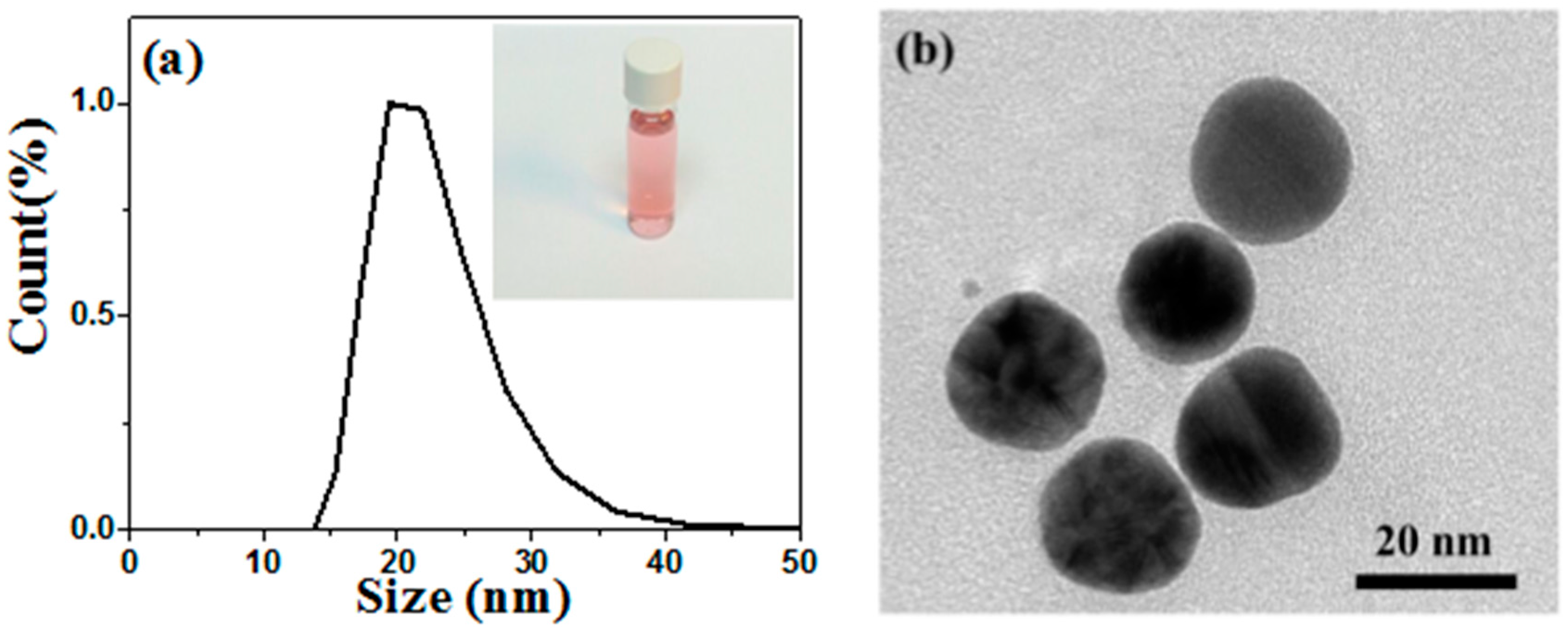
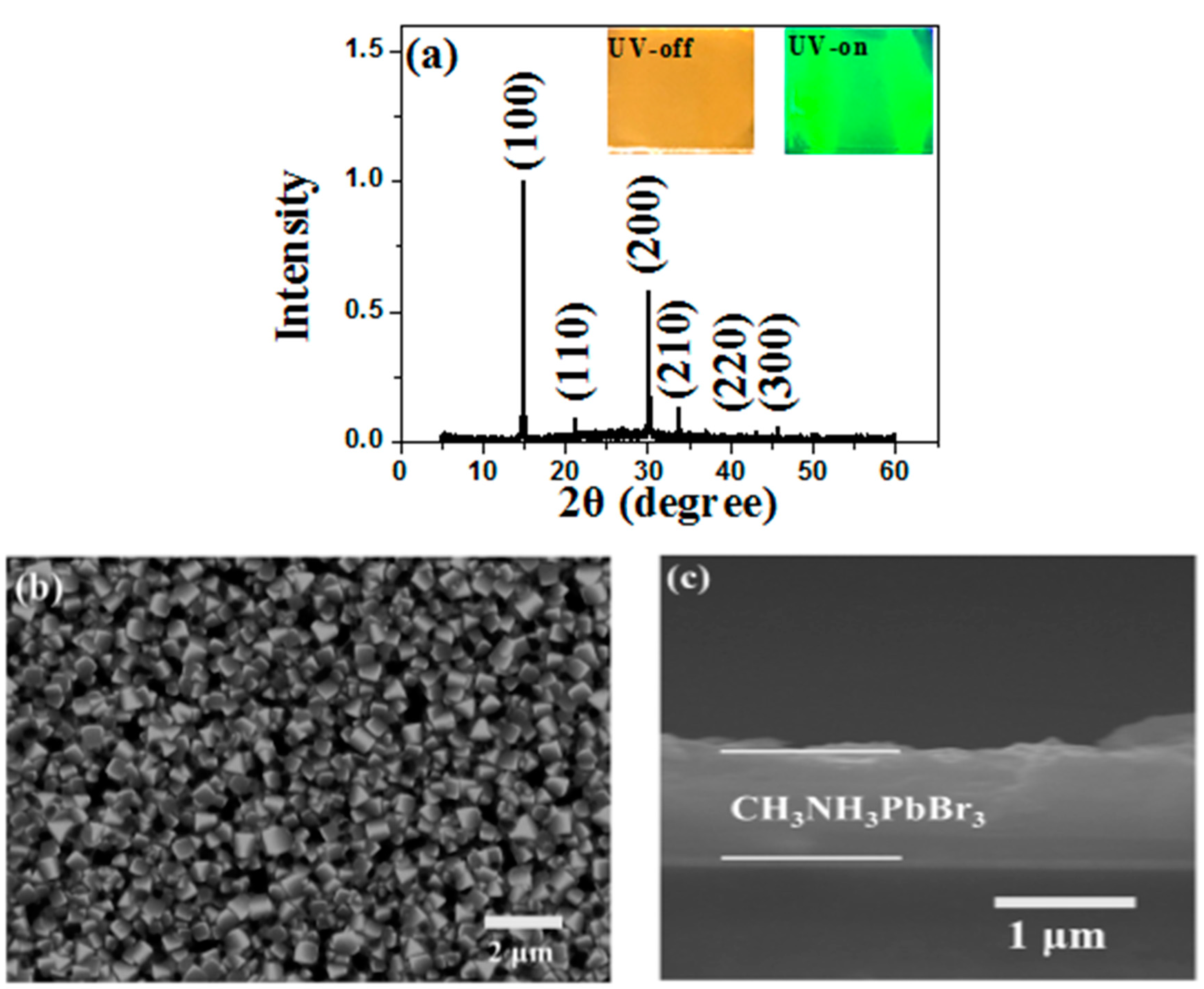
In order to investigate the ASE performance, the slab waveguide device structure with Quartz/PEDOT: PSS (with or w/o Au NPs)/MAPbBr3 (Scheme 1) was made. The experimental optical path for the ASE test is also shown in Scheme 1. Light scattering data for Au NPs size distribution showed a mean diameter of 20 nm in Figure 1a, which is well matched to the TEM images (Figure 1b). The XRD pattern shown in Figure 2a showed MAPbBr3 crystal film diffraction peaks at 14.90° (100), 21.08° (110), 29.98° (200), 33.62° (210), 36.92° (211), 42.94° (220) and 45.68° (300). The XRD data indicated pure perovskite phase, which suggested a lamellar structure PbBr2 2D-layer parallel to the substrate [39]. In Figure 2a, the inset images display the MAPbBr3 film photographs (spin-coated on quartz/PEDOT: PSS) before and after ~365 nm UV lamp irradiation, respectively, and show a smooth surfaces. Top-view and cross-section SEM images of MAPbBr3 can be seen in Figure 2b,c, respectively. The MAPbBr3 film coverage shows an average 300–500 nm grain size with highly uniform and dense stacking. Such high-quality film is critical for generating ASE phenomena [33].

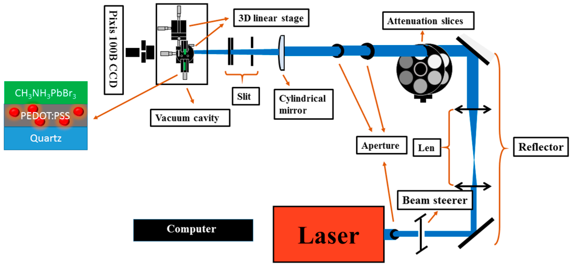
Scheme 1.
The ASE test experimental optical path and the device structure.
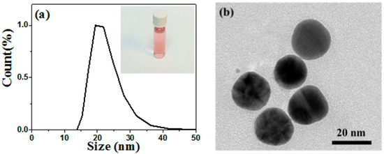
Figure 1.
(a) Light scattering data for Au NPs size distribution, inset: Au NPs solution. (b) TEM image of Au NPs.

Figure 2.
(a) XRD spectrum of MAPbBr3 crystal film, inset: image of MAPbBr3 film when UV-365 nm off and on, (b,c) Top view and cross-section SEM images of MAPbBr3 film.
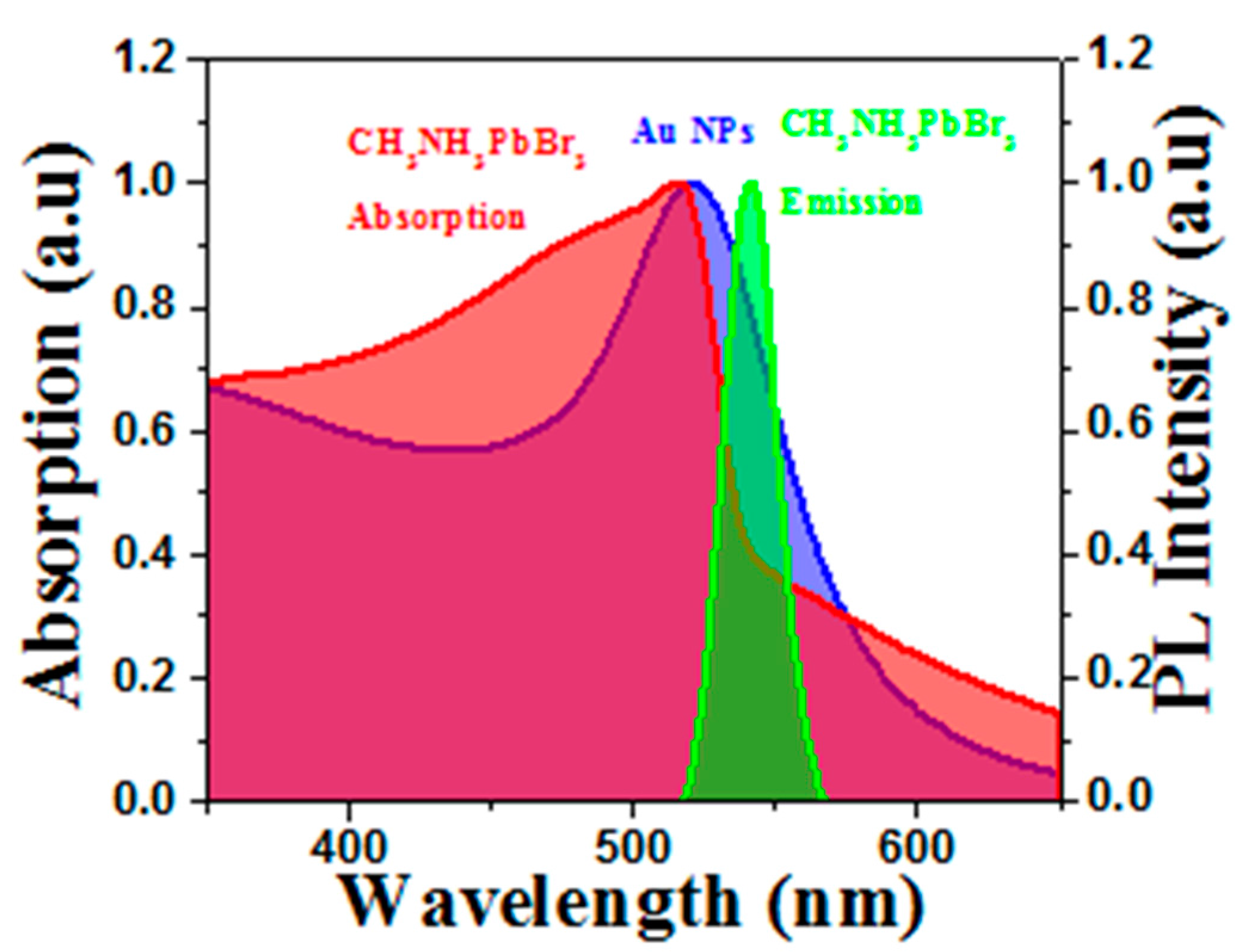
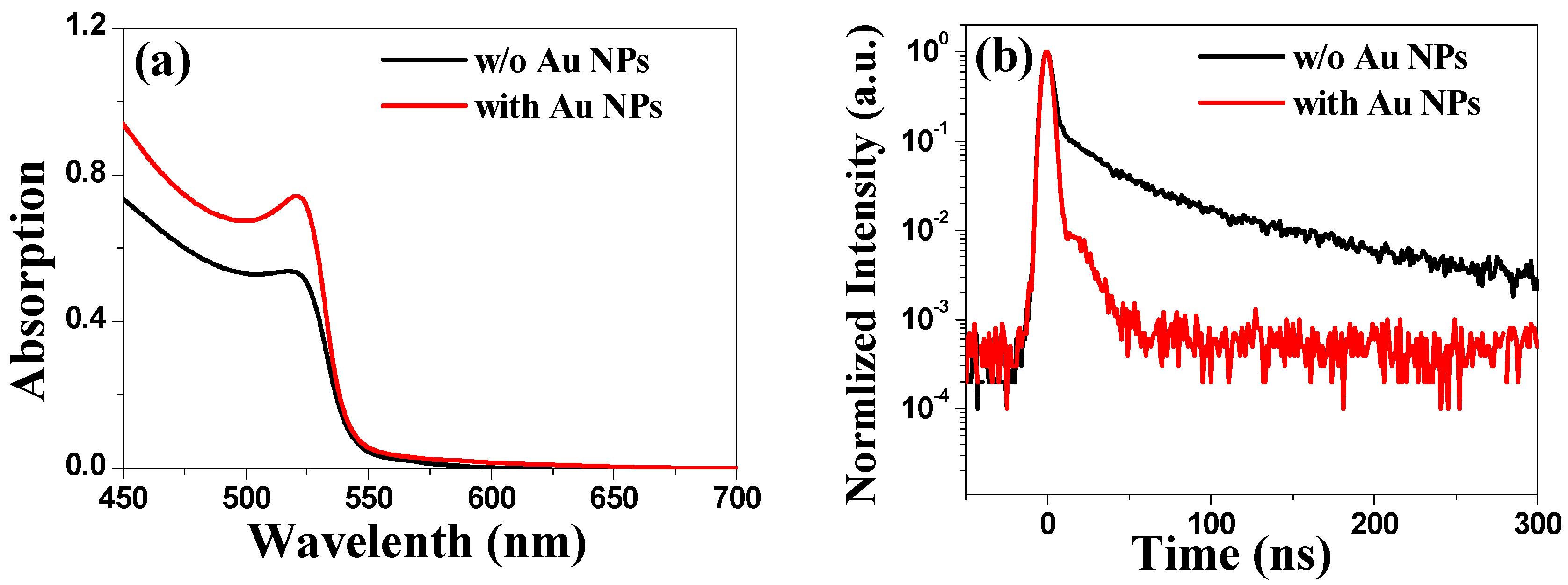
Figure 3 shows the normalized absorption and PL spectrum of MAPbBr3 film and extinction spectrum of the Au NPs solution. The absorption spectrum of MAPbBr3 shows 350 nm to 650 nm, which matches the 520 nm extinction peak of the Au NPs. The MAPbBr3 PL spectrum has its central wavelength peak at around 534 nm, with a full width at half maximum (FWHM) at ~24 nm, which also overlaps with the Au NP extinction peak. The overlap of the spectra indicates that surface plasmon resonance would induce an effective absorption or emission enhancement [40,41].

Figure 3.
Absorption spectra of MAPbBr3 film and Au NPs aqueous solution, PL spectrum of MAPbBr3 film.
The ASE emission spectra are taken as a function of optical pump energy in the device structure Quartz/PEDOT: PSS (with Au NPs)/MAPbBr3, where Quartz/PEDOT: PSS (w/o Au NPs)/MAPbBr3 acts as control device. Figure 4a shows the typical ASE behavior of the control device [12], showing a significant dependence of the edge emission spectrum with increased pump energy intensity. When the device is optically pumped under low energy, it exhibits a broad ASE emission spectrum, with a FWHM of ~30 nm in the control device. Once the excitation energy is high enough, the ASE emission spectrum becomes much narrower, with FWHM ~7 nm. The emission intensity and FWHM with and w/o Au NP doping are compared, as shown in Figure 4a–d. Figure 4c,d shows the ASE intensity and FWHM, which are taken as a function of the optical pump energy curve. The ASE intensity of the device with Au NPs shows a 16-fold enhancement compared to the control one (Figure 4c). The FWHM narrows from 7.0 to 6.4 nm, which also shows an obvious narrowing after doping with Au NPs (Figure 4d).
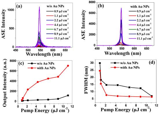
Figure 4.
The emission spectrum Device Quartz/PEDOT: PSS/MAPbBr3 (a) w/o Au NPs, (b) with Au NPs. The ASE peak intensity and FWHM of the emission spectra as a function of the pump energy (c) w/o Au NPs, (d) with Au NPs.
Figure 5a,b shows the absorbance and time-resolved PL spectra, in order to demonstrate the mechanism of ASE intensity enhancement by Au NPs. On one hand, due to the improved absorbance probability, the absorbance intensity of MAPbBr3 improved by 38% after Au NP doping (Figure 5a) [42]. Thus, the density of the excitons’ excited state is increased. On the other hand, the MAPbBr3 time-resolved PL spectrum in Figure 5b shows that the exciton lifetime of 8.23 ns in the control devices surprisingly decreases to 0.28 ns with Au NPs, which means that the radiative decay process is also accelerated.
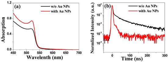
Figure 5.
(a) UV-vis spectra, (b) time-resolved PL spectra in the devices’ structure: Quartz/PEDOT: PSS/MAPbBr3 (with and w/o Au NPs).
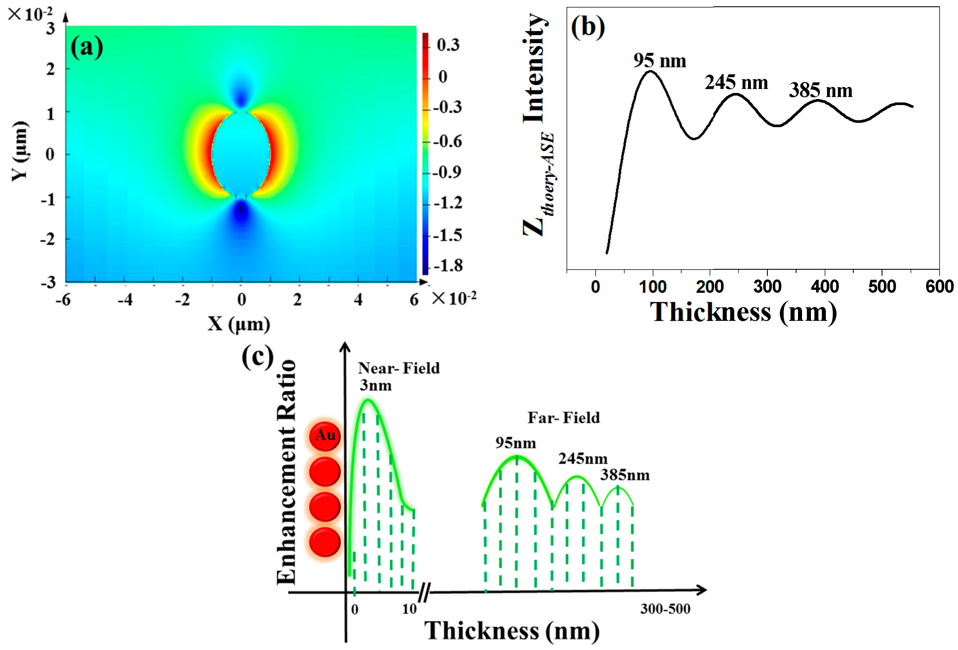
The enhancement mechanism could be contributed to the Au NP compound’s near- and far-field effects. The near- and far-field distributions are simulated as shown in Figure 6a,b. For near-field, Figure 6a shows that the working distance is within the range of 1–10 nm, as simulated by FDTD around the neighborhood of Au NPs. The intensity degraded with distance very quickly, and nearly vanished beyond 10 nm. The thickness of PEDOT: PSS is the key factor for determining the improvements of ASE intensity. The thin PEDOT: PSS thickness would induce Au NP contact with MAPbBr3, which could directly quench the fluorescence by Förster energy transfer [43,44]. The thick PEDOT: PSS would hinder the near-field effect. In our research work, the thickness of PEDOT: PSS is optimized at 23 nm, which would make full use of near-field. For far-field, the detailed mechanism was described in the Experimental Section. Based on the simulated far-field classic model, Figure 6b displays the main improved multi-enhancement peaks. The main improved peaks are 95 nm, 245 nm and 385 nm, which are within the scope of the MAPbBr3 thickness of 500 nm. Considering the device structure and the thickness of MAPbBr3 and PEDOT: PSS, the near- and far-field could both overlap with the gain medium, as shown in Figure 6c. There are two advantages to using compound near- and far-field surface plasmon resonance, in comparison to a single optical effect: (1) the enhancement ratio of ASE intensity using compound surface plasmon resonance would be greater than with a single-optical effect; and (2) considering the device structure (shown in Scheme 1), it’s easy to utilize compound surface plasmon resonance in lasing devices based on perovskites.
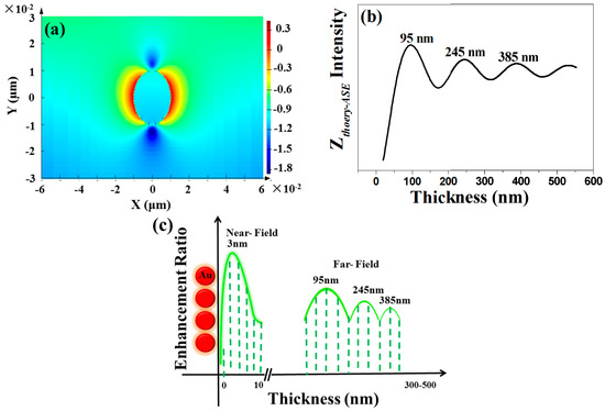
Figure 6.
Theoretical simulation of (a) near-electric field profile, (b) far-field, (c) distribution in devices.
4. Conclusions
In summary, we demonstrated an obvious performance improvement of lasing devices by doping Au NPs into the optically pumped slab waveguide device. The ASE intensity and FWHM were both effectively promoted. The results indicate that the compound near- and far-field surface plasmon resonance is the mechanism of enhancement, both of which could increase the density of the excitons’ excited state and accelerate the radiative decay process. Our results provide a flexible and effective route for obtaining high-performance lasing devices based on perovskites.
Acknowledgments
This work was supported by the National Natural Science Foundation of China (Grant No. 51473052, 11504300, 11602243), NSFA of China (Grant No. U1630125), Natural Science Foundation Project of CQ CSTC (Grant No. cstc2015jcyjA50002).
Author Contributions
Xiaoyan Wu designed the experiments; Xiaoyan Wu, Yanglong Li, Wei Li, Lingyuan Wu, Bo Fu performed the experiments; Xiaoyan Wu, Weiping Wang, Dayong Zhang and Ping Chen analyzed the data; Guodong Liu and Jianheng Zhao supervised the project.
Conflicts of Interest
The authors declare no conflict of interest.
References
- Veldhuis, S.A.; Boix, P.P.; Yantara, N.; Li, M.J.; Sum, T.C.; Mathews, N.; Mhaisalkar, S.G. Perovskite Materials for Light-Emitting Diodes and Lasers. Adv. Mater. 2016, 28, 6804–6834. [Google Scholar] [CrossRef] [PubMed]
- Schmidt, L.C.; Pertegás, A.; González-Carrero, S.; Malinkiewicz, O.; Agouram, S.; Mínguez Espallargas, G.; Bolink, H.J.; Galian, R.E.; Pérez-Prieto, J. Nontemplate. Synthesis of CH3NH3PbBr3 Perovskite Nanoparticles. J. Am. Chem. Soc. 2014, 136, 850–852. [Google Scholar] [CrossRef] [PubMed]
- Tan, Z.K.; Moghaddam, R.S.; Lai, M.L.; Docampo, P.; Higler, R.; Deschler, F.; Price, M.; Sadhanala, A.; Pazos, L.M.; Credgington, D.; et al. Bright Light-Emitting Diodes Based on Organometal Halide Perovskite. Nat. Nanotechnol. 2014, 9, 687–692. [Google Scholar] [CrossRef] [PubMed]
- Yadav, P.; Prochowicz, D.; Saliba, M.; Boix, P.P.; Zakeeruddin, S.M.; Grätzel, M. Interfacial Kinetics of Efficient Perovskite Solar Cells. Crystals 2017, 7, 252. [Google Scholar] [CrossRef]
- Kim, Y.; Cho, H.; Heo, J.H.; Kim, T.; Myoung, N.; Lee, C.; Im, S.H.; Lee, T. Multicolored Organic/Inorganic Hybrid Perovskite Light-Emitting Diodes. Adv. Mater. 2015, 27, 1248–1254. [Google Scholar] [CrossRef] [PubMed]
- Feng, J.G.; Yan, X.X.; Zhang, Y.F.; Wang, X.D.; Wu, Y.C.; Su, B.; Fu, H.B.; Jiang, L. “Liquid Knife” to Fabricate Patterning Single-Crystalline Perovskite Microplates toward High-Performance Laser Arrays. Adv. Mater. 2016, 28, 3732–3741. [Google Scholar] [CrossRef] [PubMed]
- Kuehne, A.J.; Gather, M.C. Organic Lasers: Recent Developments on Materials, Device Geometries, and Fabrication Techniques. Chem. Rev. 2016, 116, 12823–12864. [Google Scholar] [CrossRef] [PubMed]
- Yang, D.C.; Xie, C.; Sun, J.H.; Zhu, H.; Xu, X.H.; You, P.; Lau, S.P.; Yan, F.; Yu, S.F. Amplified Spontaneous Emission from Organic-Inorganic Hybrid Lead Iodide Perovskite Single Crystals under Direct Multiphoton Excitation. Adv. Opt. Mater. 2016, 4, 1053–1059. [Google Scholar] [CrossRef]
- Yu, Z.Y.; Wu, Y.S.; Liao, Q.; Zhang, H.H.; Bai, S.M.; Li, H.; Xu, Z.Z.; Sun, C.L.; Wang, X.D.; Yao, J.N.; Fu, H.B. Self-Assembled Microdisk Lasers of Perylenediimides. J. Am. Chem. Soc. 2015, 137, 15105–15111. [Google Scholar] [CrossRef] [PubMed]
- Stehr, J.; Crewett, J.; Schindler, F.; Sperling, R.; Holleitner, A.W. A Low Threshold Polymer Laser Based on Metallic Nanoparticles Gratings. Adv. Mater. 2003, 15, 1726–1729. [Google Scholar] [CrossRef]
- Tessler, N.; Harrison, N.T.; Friend, R.H. High Peak Brightness Polymer Light-Emitting Diodes. Adv. Mater. 1998, 10, 64–68. [Google Scholar] [CrossRef]
- Xing, G.C.; Mathews, N.; Lim, S.S.; Natalia, Y.; Liu, X.F.; Sabba, D.; Grätzel, M.; Mhaisalkar, S.; Sum, T.C. Low-temperature solution-processed wavelength-tunable perovskites for lasing. Nat. Mater. 2014, 13, 476–480. [Google Scholar] [CrossRef] [PubMed]
- Zhu, H.M.; Fu, Y.P.; Meng, F.; Wu, X.X.; Gong, Z.Z.; Ding, Q.; Gustaffson, M.V.; Trinh, T.M.; Jin, S.; Zhu, X.Y. Lead halide perovskite nanowire lasers with low lasing thresholds and high quality factors. Nat. Mater. 2015, 14, 636–642. [Google Scholar] [CrossRef] [PubMed]
- Deschler, F.; Price, M.; Pathak, S.; Klintberg, L.E.; Jarausch, D.D.; Higler, R.; Hüttner, S.; Leijtens, T.; Stranks, S.D.; Snaith, H.J.; et al. High Photoluminescence Efficiency and Optically Pumped Lasing in Solution-Processed Mixed Halide Perovskite Semiconductors. J. Phys. Chem. Lett. 2014, 5, 1421–1426. [Google Scholar] [CrossRef] [PubMed]
- Zhang, C.; Wang, K.Y.; Yi, N.B.; Gao, Y.S.; Zhu, M.X.; Sun, W.Z.; Liu, S.; Xu, K.; Xiao, S.M.; Song, Q.H. Improving the Performance of a CH3NH3PbBr3 Perovskite Microrod Laser through Hybridization with Few-Layered Graphene. Adv. Opt. Mater. 2016, 4, 2057–2062. [Google Scholar] [CrossRef]
- Wang, Y.; Li, X.M.; Zhao, X.; Xiao, L.; Zeng, H.B.; Sun, H.D. Nonlinear Absorption and Low-Threshold Multiphoton Pumped Stimulated Emission from All-Inorganic Perovskite Nanocrystals. Nano. Lett. 2016, 16, 448–453. [Google Scholar] [CrossRef] [PubMed]
- Li, X.L.; Guo, Y.; Luo, B.B. Improved Stability and Photoluminescence Yield of Mn2+-Doped CH3NH3PbCl3 Perovskite Nanocrystals. Crystals 2018, 8, 4. [Google Scholar] [CrossRef]
- Li, Y.H.; Zhang, T.Y.; Xu, F.; Wang, Y.; Li, G.; Yang, Y.; Zhao, Y.X. CH3NH3Cl Assisted Solvent Engineering for Highly Crystallized and Large Grain Size Mixed-Composition (FAPbI3)0.85(MAPbBr3)0.15 Perovskites. Crystals 2017, 7, 272. [Google Scholar] [CrossRef]
- Saliba, M.; Wood, S.M.; Patel, J.B.; Nayak, P.K.; Huang, J.; Alexander-Webber, J.A.; Wenger, B.; Stranks, S.D.; Hörantner, M.T.; Wang, J.T.W.; et al. Structured Organic-Inorganic Perovskite toward a Distributed Feedback Laser. Adv. Mater. 2016, 28, 923–929. [Google Scholar] [CrossRef] [PubMed]
- Liu, Y.L.; Fang, C.Y.; Yu, C.C.; Yang, T.C.; Chen, H.L. Controllable Localized Surface Plasmonic Resonance Phenomena in Reduced Gold Oxide Films. Chem. Mater. 2014, 26, 1799–1806. [Google Scholar] [CrossRef]
- Li, Y.F.; Feng, J.; Dong, F.X.; Ding, R.; Zhang, Z.Y.; Zhang, X.L.; Chen, Y.; Bi, Y.G.; Sun, H.B. Surface plasmon-enhanced amplified spontaneous emission from organic single crystals by integrating graphene/copper nanoparticle hybrid nanostructures. Nanoscale 2017, 9, 19353–19359. [Google Scholar] [CrossRef] [PubMed]
- Li, Y.L.; Ye, Y.; Fan, Y.D.; Zhou, J.; Jia, L.; Tang, B.; Wang, X.G. Silver Nanoprism-Loaded Eggshell Membrane: A Facile Platform for In Situ SERS Monitoring of Catalytic Reactions. Crystals 2017, 7, 45. [Google Scholar] [CrossRef]
- Su, Y.H.; Ke, Y.F.; Cai, S.L.; Yao, Q.Y. Surface plasmon resonance of layer-by-layer gold nanoparticles induced photoelectric current in environmentally-friendly plasmon-sensitized solar cell. Light Sci. Appl. 2012, 1, e14. [Google Scholar] [CrossRef]
- Gu, M.; Li, X.P.; Cao, Y.Y. Optical storage arrays: A perspective for future big data storage. Light Sci. Appl. 2014, 3, e177. [Google Scholar] [CrossRef]
- Wu, X.Y.; Liu, L.L.; Choy, W.C.H.; Yu, T.C.; Cai, P.; Gu, Y.J.; Xie, Z.Q.; Zhang, Y.N.; Du, L.Y.; Mo, Y.Q.; et al. Substantial performance improvement in inverted polymer light-emitting diodes via surface plasmon resonance induced electrode quenching control. ACS Appl. Mater. Interfaces 2014, 6, 11001–11006. [Google Scholar] [CrossRef] [PubMed]
- Wu, X.Y.; Liu, L.L.; Yu, T.C.; Yu, L.; Xie, Z.Q.; Mo, Y.Q.; Xu, S.P.; Ma, Y.G. Gold nanoparticles modified ITO anode for enhanced PLEDs brightness and efficiency. J. Mater. Chem. C 2013, 1, 7020–7025. [Google Scholar] [CrossRef]
- Wu, X.Y.; Liu, L.L.; Deng, Z.C.; Nian, L.; Zhang, W.Z.; Hu, D.H.; Xie, Z.Q.; Mo, Y.Q.; Ma, Y.G. Efficiency improvement in polymer light-emitting diodes by “far-field” effect of gold nanoparticles. Part. Part. Syst. Charact. 2015, 32, 686–692. [Google Scholar] [CrossRef]
- Wu, X.Y.; Zhuang, Y.Q.; Feng, Z.T.; Zhou, X.H.; Yang, Y.Z.; Liu, L.L.; Xie, Z.Q.; Chen, X.D.; Ma, Y.G. Simultaneous red-green-blue electroluminescent enhancement directed by surface plasmonic “far-field” of facile gold nanospheres. Nano Res. 2018, 11, 151–162. [Google Scholar] [CrossRef]
- Wang, J.Y.; Hsu, F.C.; Huang, J.Y.; Wang, L.; Chen, Y.F. Bifunctional Polymer Nanocomposites as Hole-Transport Layers for Efficient Light Harvesting: Application to Perovskite Solar Cells. ACS Appl. Mater. Interfaces 2015, 7, 27676–27684. [Google Scholar] [CrossRef] [PubMed]
- Lee, D.S.; Kim, W.; Cha, B.G.; Kwon, J.; Kim, S.J.; Kim, M.; Kim, J.; Wang, D.H.; Park, J.H. Self-Position of Au NPs in Perovskite Solar Cells: Optical and Electrical Contribution. ACS Appl. Mater. Interfaces 2016, 8, 449–454. [Google Scholar] [CrossRef] [PubMed]
- Balakrishnan, S.K.; Kamat, P.V. Au-CsPbBr3 Hybrid Architecture: Anchoring Gold Nanoparticles on Cubic Perovskite Nanocrystals. ACS Energy Lett. 2017, 2, 88–93. [Google Scholar] [CrossRef]
- Zhang, X.; Xu, B.; Wang, W.; Liu, S.; Zheng, Y.; Chen, S.; Wang, K.; Sun, X.W. Plasmonic Perovskite Light-Emitting Diodes Based on the Ag-CsPbBr3 System. ACS Appl. Mater. Interfaces 2017, 9, 4926–4931. [Google Scholar] [CrossRef] [PubMed]
- Chen, P.; Xiong, Z.Y.; Wu, X.Y.; Shao, M.; Meng, Y.; Xiong, Z.H.; Gao, C.H. Nearly 100% Efficiency Enhancement of CH3NH3PbBr3 Perovskite Light-Emitting Diodes by Utilizing Plasmonic Au Nanoparticles. J. Phys. Chem. Lett. 2017, 8, 3961–3969. [Google Scholar] [CrossRef] [PubMed]
- Frens, G. Controlled Nucleation for the Regulation of the Particle Size in Monodisperse Gold Suspensions. Nat. Phys. Sci. 1973, 241, 20–22. [Google Scholar] [CrossRef]
- Wu, X.Y.; Li, Y.L.; Wu, L.Y.; Fu, B.; Liu, G.D.; Zhang, D.Y.; Zhao, J.H.; Chen, P.; Liu, L.L. Enhancing perovskite film fluorescence by simultaneous near-and far-field effects of gold nanoparticles. RSC Adv. 2017, 7, 35752–35756. [Google Scholar] [CrossRef]
- Kummerlen, J.; Leitner, A.; Brunner, H.; Aussenegg, F.R.; Wokaun, A. Enhanced dye fluorescence over silver island films: Analysis of the distance dependence. Mol. Phys. 1993, 80, 1031–1046. [Google Scholar] [CrossRef]
- Kuhn, H. Classical Aspects of Energy Transfer in Molecular Systems. J. Chem. Phys. 1970, 53, 101–108. [Google Scholar] [CrossRef]
- Drexhage, K.H. Influence of a dielectric interface on fluorescence decay time. J. Lumin. 1970, 1, 693–701. [Google Scholar] [CrossRef]
- Yang, B.; Mao, X.; Yang, S.Q.; Li, Y.J.; Wang, Y.Q.; Wang, M.S.; Deng, W.Q.; Han, K.L. Low Threshold Two-Photon-Pumped Amplified Spontaneous Emission in CH3NH3PbBr3 Microdisks. ACS Appl. Mater. Interfaces 2016, 8, 19587–19592. [Google Scholar] [CrossRef] [PubMed]
- Wu, X.Y.; Liu, L.L.; Xie, Z.Q.; Ma, Y.G. Advance in Metal-based Nanoparticles for the Enhanced Performance of Organic Optoelectronics Devices. Chem. J. Chin. Univ. 2016, 37, 409–425. [Google Scholar]
- Choi, H.; Ko, S.J.; Choi, Y.; Joo, P.; Kim, T.; Lee, B.R.; Jung, J.W.; Choi, H.J.; Cha, M.; Jeong, J.R.; et al. Versatile surface plasmon resonance of carbon-dot-supported silver nanoparticles in polymer optoelectronic devices. Nat. Photonics 2013, 7, 732–738. [Google Scholar] [CrossRef]
- Stratakis, E.; Kymakis, E. Nanoparticle-based plasmonic organic photovoltaic devices. Mater. Today 2013, 16, 133–146. [Google Scholar] [CrossRef]
- Xiao, Y.; Yang, J.P.; Cheng, P.P.; Zhu, J.J.; Xu, Z.Q.; Deng, Y.H.; Lee, S.T.; Li, Y.Q.; Tang, J.X. Surface plasmon-enhanced electroluminescence in organic light-emitting diodes incorporating Au nanoparticles. Appl. Phys. Lett. 2012, 100, 013308–013311. [Google Scholar] [CrossRef]
- Kim, T.; Kang, H.; Jeong, S.; Kang, D.J.; Lee, C.; Lee, C.H.; Seo, M.K.; Lee, J.Y.; Kim, B. Au@Polymer Core-Shell Nanoparticles for Simultaneously Enhancing Efficiency and Ambient Stability of Organic Optoelectronic Devices. ACS Appl. Mater. Interfaces 2014, 6, 16956–16965. [Google Scholar] [CrossRef] [PubMed]

© 2018 by the authors. Licensee MDPI, Basel, Switzerland. This article is an open access article distributed under the terms and conditions of the Creative Commons Attribution (CC BY) license (http://creativecommons.org/licenses/by/4.0/).