Article

A Feasible and Effective Post-Treatment Method for High-Quality CH3NH3PbI3 Films and High-Efficiency Perovskite Solar Cells

Key Lab of Material Physics, Department of Physics and Engineering, Zhengzhou University, Zhengzhou 450052, China
*
Author to whom correspondence should be addressed.
Crystals 2018, 8(1), 44; https://doi.org/10.3390/cryst8010044
Submission received: 14 December 2017 / Revised: 13 January 2018 / Accepted: 13 January 2018 / Published: 18 January 2018

Abstract

:
The morphology control of CH3NH3PbI3 (MAPbI3) thin-film is crucial for the high-efficiency perovskite solar cells, especially for their planar structure devices. Here, a feasible and effective post-treatment method is presented to improve the quality of MAPbI3 films by using methylamine (CH3NH2) vapor. This post-treatment process is studied thoroughly, and the perovskite films with smooth surface, high preferential growth orientation and large crystals are obtained after 10 s treatment in MA atmosphere. It enhances the light absorption, and increases the recombination lifetime. Ultimately, the power conversion efficiency (PCE) of 15.3% for the FTO/TiO2/MAPbI3/spiro-OMeTAD/Ag planar architecture solar cells is achieved in combination with this post-treatment method. It represents a 40% improvement in PCE compared to the best control cell. Moreover, the whole post-treatment process is simple and cheap, which only requires some CH3NH2 solution in absolute ethanol. It is beneficial to control the reaction rate by changing the volume of the solution. Therefore, we are convinced that the post-treatment method is a valid and essential approach for the fabrication of high-efficiency perovskite solar cells.

Graphical Abstract

1. Introduction

In recent years, hybrid organic-inorganic perovskite solar cells (PSCs) have developed rapidly. The power conversion efficiencies (PCEs) of these PSCs span from 3.8% [1] to a verified PCE of 22.7% [2], stems from a number of remarkable properties, including high absorption coefficient (~104 cm−1) [3,4], low exciton binding energy (<100 MeV) [5,6,7], long charge carrier diffusion length (102–105 nm) [8,9,10,11] and high charge carrier mobility (10–102 cm2 V−1 s−1) [12,13,14,15]. In addition, organometallic halide perovskite is suitable for solution and low temperature fabrication, because the precursor material in several organic solvents (dimethyl sulfoxide (DMSO), N,N-Methylformamide (DMF), γ-butyrolactone (γ-GBL), etc.) has a perfect solubility [16,17,18,19]. Multifarious methods are successfully used to improve the efficiencies of PSCs, including interface engineering [20,21], compositional engineering [22], solvent engineering [23], new materials [24] and device structure modification [25], etc. Among them, which one is more effective is indistinguishable.
To date, the PCE of PSCs has been enhanced by minimizing charge recombination in bulk perovskite film and/or at the interfaces between perovskite and charge transport layers. The reduction of charge recombination in bulk film requires high quality perovskite film with full surface coverage [26,27,28], large crystal size [15,29,30] and low defect density [31,32,33]. The post-treatment using a strong Lewis base is a very effective method to improve the quality of lead halide perovskite films [34,35,36,37,38,39,40,41,42]. In 2014, Zhao et al. [34] first found a room-temperature phase transformation of CH3NH3PbI3 induced by ammonia. After one year, Zhou et al. [35] reported CH3NH2 (MA) induced defect-healing (MIDH) of MAPbI3 perovskite thin films based on the formation of MAPbI3·xMA intermediate, resulting in an ultra-smooth and dense film with a higher degree of crystallinity and texture. Chih et al. [36] also certified that the post-treatment by MA gas promotes the regrowth of MAPbBr3 crystallites following the preferred orientations and significantly enhances the film quality and photoluminescence properties. Zhao et al. [38] thoroughly studied the post-treatment process, and provided design rules for the broad, rational extension of this process to new systems and scales. Jiang et al. [39] introduced MA gas to eliminate grain boundaries and gaps, and Jacobs et al. [40] employed a thermally induced recrystallization of MAPbI3 during the liquidation process to enhance grain size. However, MA gas is supplied mainly through a solid reaction between MACl and KOH powders at room temperature, which is more complex and expensive. In this paper, commercially cheap methylamine solution in absolute ethanol is used directly to supply MA vapor, and the quality of MAPbI3 perovskite films can be optimized feasibly by changing the post-treatment times in MA atmosphere. Only after 10 s treatment can the perovskite films with surface smoothness, compact structure and preferential orientation in (110) planes be obtained, which obviously improves the photoluminescence properties and carrier extraction efficiency of perovskite. Introducing this post-treatment method in the PSCs fabrication process, the PCE of FTO/TiO2/MAPbI3/spiro-OMeTAD/Ag planar heterojunction device is increased by 40% compared to the control devices without treatment.

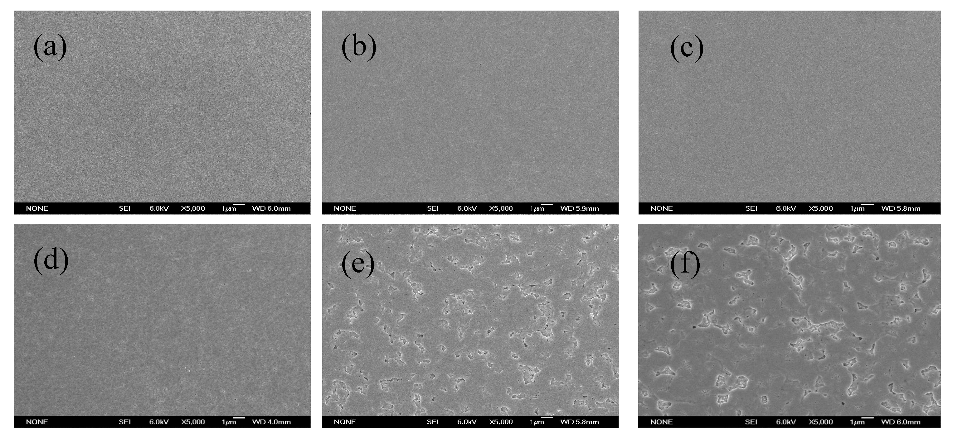
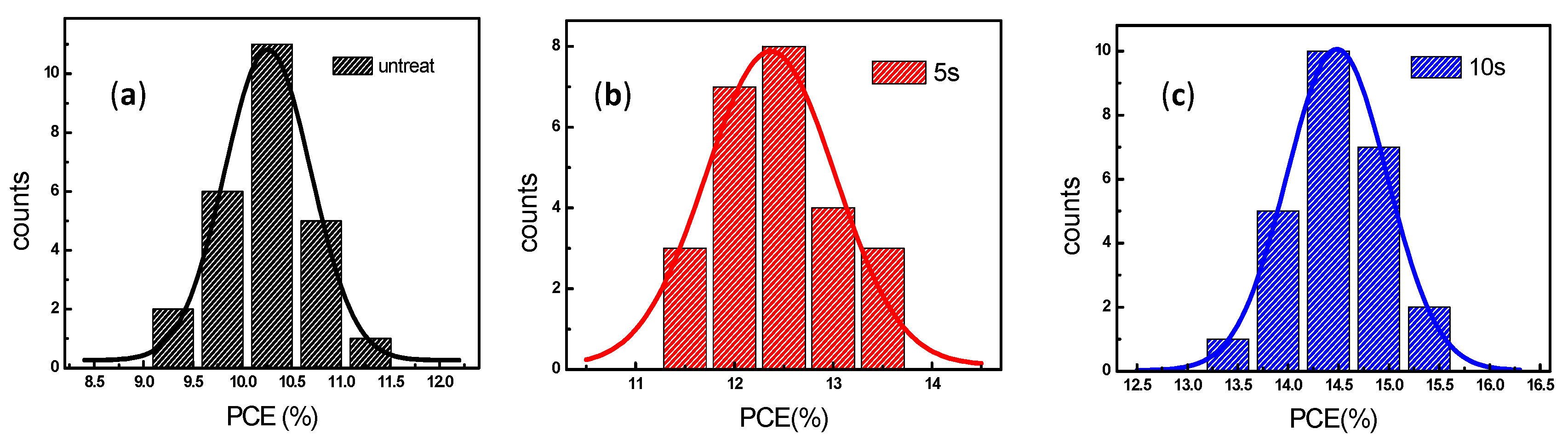
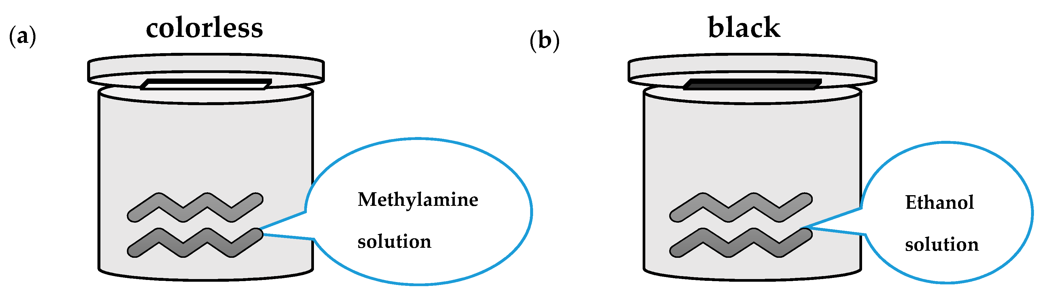
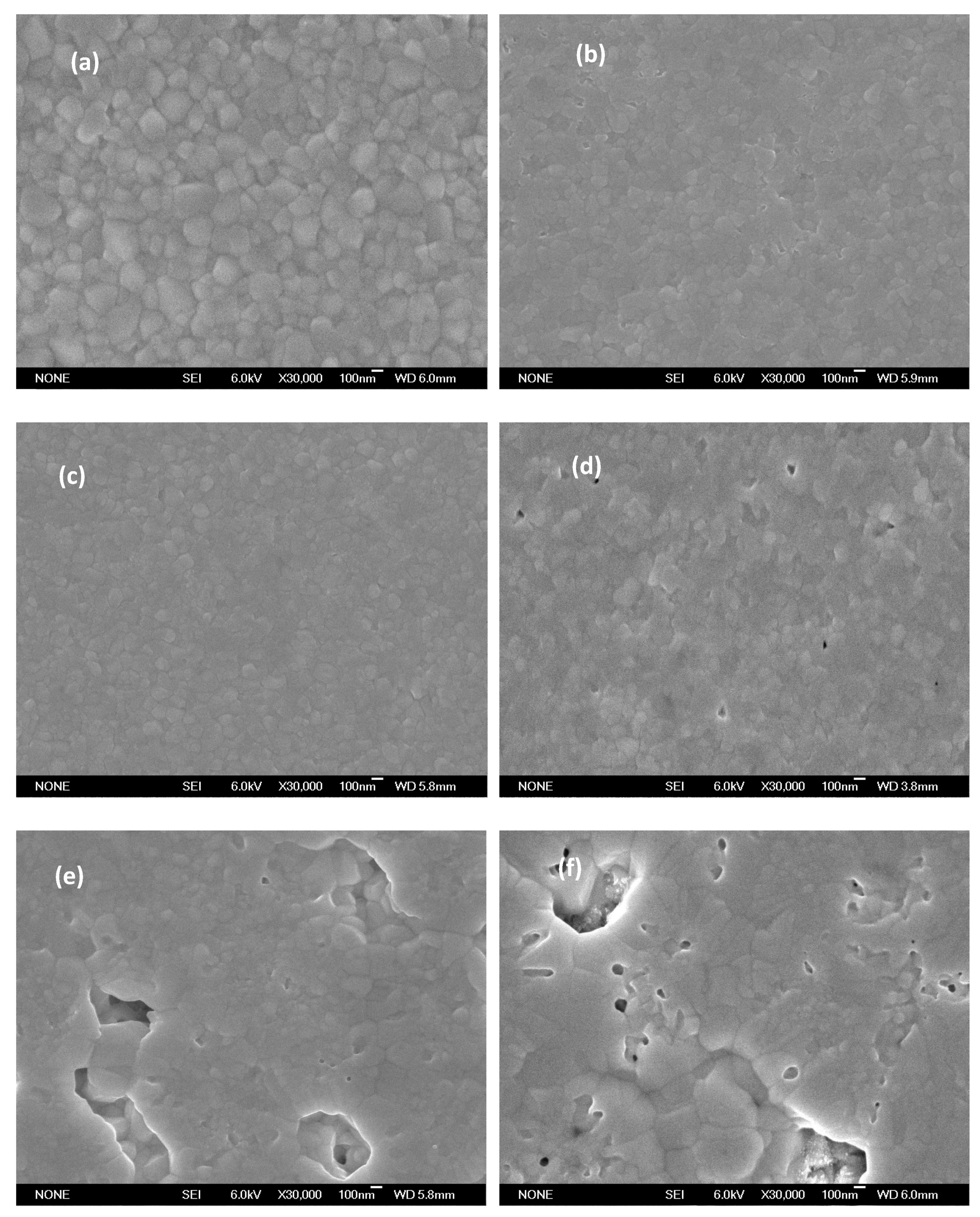
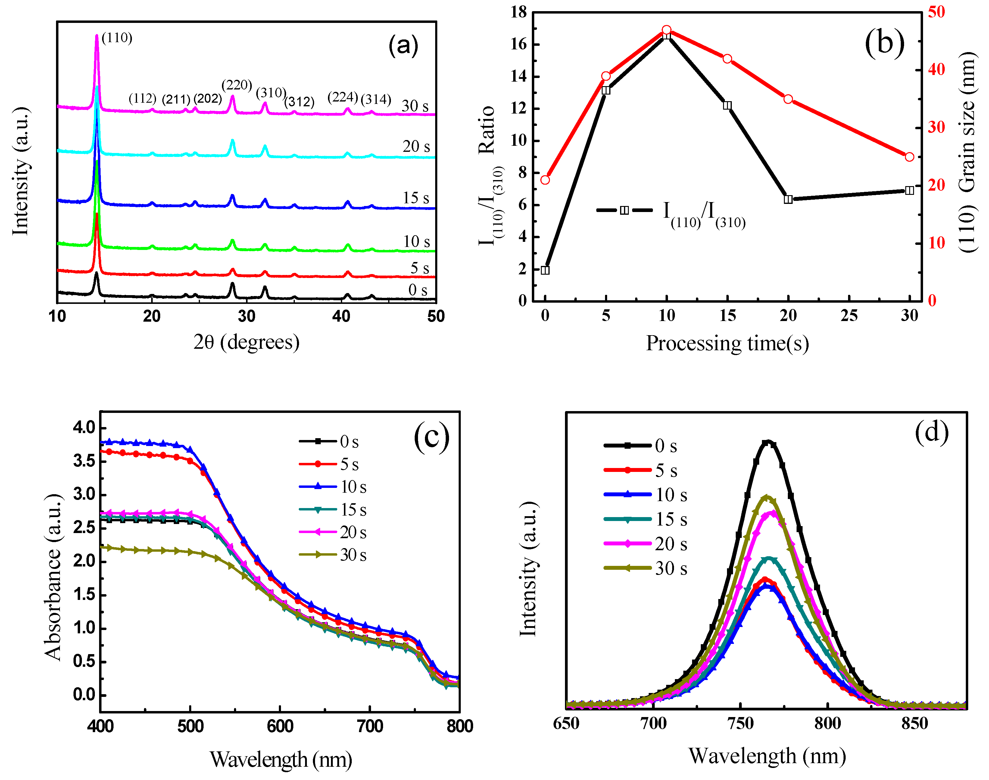
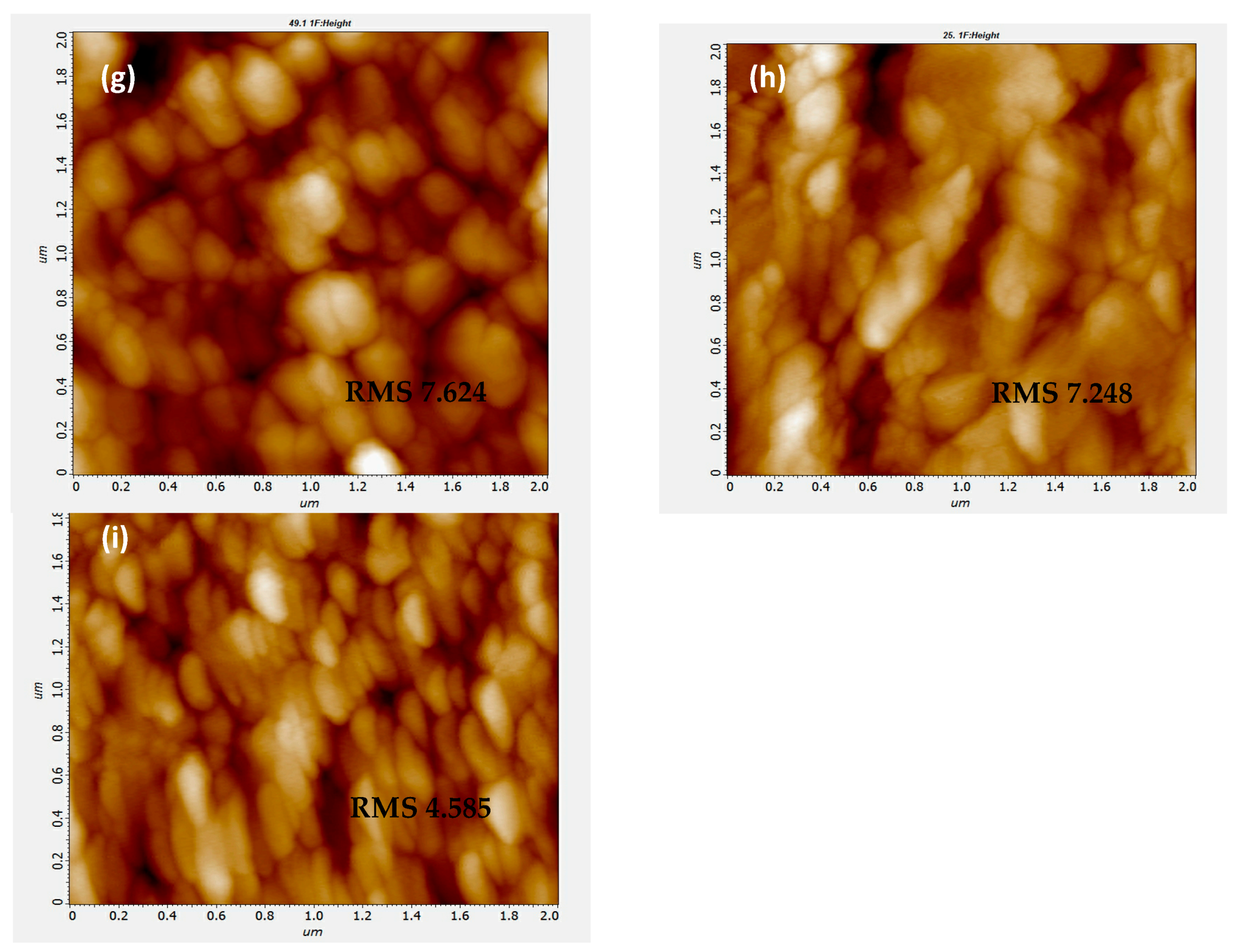
2. Results and Discussion

Figure 1a presents the X-ray diffraction (XRD) spectrum of MAPbI3 films with different treatment times in MA gas. The XRD patterns of as-deposited MAPbI3 film without MA gas treating (0 s) exhibits a main peak at 14.2, which is the characteristic of (110) plane in the tetragonal crystal structure, with other peaks corresponding to the (112), (211), (202), (220), (310), (312), (224), and (314) planes in the plot. The positions of these peaks are accorded with the results published previously [29]. The XRD intensity of (110) peak increases seven-fold with 5 s treating and nine-fold with 15 s treating approximately compared to that without MA treating, then decreases, further extending the MA treatment time. However, as shown in Figure 1a, the intensities of (220) and (310) peaks decrease firstly and then increase with prolonging the time. They ultimately reach the minimum value at 5 s treatment. The XRD intensity ratio of (110) and (310) peaks (I(110)/I(310)) with MA treatment time is shown in Figure 1b, and a maximum ratio is obtained with 10 s treatment. This suggests that the regrowth of MAPbI3 crystallites by MA gas treating prefers the formation of (110) planes on the substrate.
The average crystal size of (110) plane deduced from Scherrer Formula is presented in Figure 1b. The crystal size showed a trend of first increasing and then decreasing with MA treatment time, which is similar to the change of I(110)/I(310) ratios. A maximum size of 47 nm is achieved with 10 s treatment, which is about twofold compared to the as-deposited film, indicating that the optimum MA treatment time is 10 s. Figure 1c shows the UV-Visible light absorbance spectra of the corresponding samples. There is a steep cutoff at the wavelength about 785 nm in accordance with a band bap of about 1.58 eV. The light absorbance at the range of 400–550 nm is more sensitive to the MA treatment time, and the largest absorbance is obtained for the sample with 10 s MA treating. The implementation of unreasonable MA treatment time results in a lower absorbance than that of the as-deposited MAPbI3 film.
Figure 1d illustrates steady-state photoluminescence (PL) measurement of MAPbI3 films deposited on FTO/TiO2 substrates. The position of the stable PL emission peaks center at ~768 nm varies with <10 MeV, which is consistent with the optical gap deduced from the absorption spectra. The PL intensity of as-deposited MAPbI3 film is very high as shown in Figure 1c, suggesting the inefficient carrier transfer at the TiO2/MAPbI3 interface. The PL intensity decreases with MA treatment time from 0 s to 10 s, and then increases with the further treating. In contrast, the PL measurement of MAPbI3 film treated with ethanol vapor, as shown in Figure A1, remains unchanged regardless of whether the post-processing time of ethanol vapor is 10 s or 30 s. This indicates that the post-treatment of ethanol vapor is not helpful for the properties of MAPbI3 film or the carrier transfer at TiO2/MAPbI3 interface. MAPbI3 film treated with 10 s MA exhibits a minimum PL intensity, which is reduced by 50% compared with the film without MA treating (0 s), indicating a more efficient carrier transfer at interface. This is directly related to the (110) preferential orientation of the perovskite film after 10 s post treatment. Wang et al. [43] reported that the preferential orientation of MAPbI3 perovskite crystal with (110) crystal plane was better for perovskite solar cells, based on synchrotron radiation two-dimensional X-ray grazing incidence diffraction. The crystallographic orientation of the (110) crystal grains is favorable for the propagation of electrons and holes, and the migration rate of the carriers, which facilitates the rapid propagation of electrons and holes along the out-of-plane direction to the electron and hole transport layer. The carriers convert into an effective photocurrent by the electrode collection, thereby enhancing the device’s photoelectric conversion performance.
The scanning electron microscopy (SEM) images of MAPbI3 film with different MA gas treatment times are shown in Figure 2a−f (see more data in Figure A2). The as-deposited MAPbI3 film is composed of densely packed grains with the domain size distributing in a range of 200–300 nm, and the crystal boundaries are visible on the surface of the polycrystalline film, in agreement with the previous report of MAPbI3 film prepared by the one-step anti-solvent method [44]. After exposing the MAPbI3 film to MA gas for 5 s, and 10 s, respectively, as shown in Figure 2b–c, the boundary interfaces become unclear, which infers that the gas-solid reaction benefits the regrowth of MAPbI3 crystallites through the grain boundaries. The corresponding tapping-mode atomic force microscope (AFM) height images in 2.0 µm × 2.0 µm area are presented in Figure 2g–i, and the root-mean-square roughness (RMS) decreases from 7.624 nm for the as-deposited sample to 4.585 nm for the perovskite with 10 s MA treating (three-dimensional images are shown Figure A3). As the post-treatment time increases to 15 s (Figure 2d), some pinholes appear on the MAPbI3 film surface. Further increasing the post-processing time to 20 s and 30 s (Figure 2e–f), the MAPbI3 film is not uniformly covered on the substrate with many voids between grains. Through the low magnification (Figure A2), the film completely covers the substrate when post-processing time is below 15 s. However, if the post-processing time is over 20 s, the substrate is exposed. Therefore, the quality of MAPbI3 film treated with MA gas is affected by post-processing times.
Figure 3a depicts the cross-sectional view of the PSC with glass/FTO/TiO2/MAPbI3/spiro-OMeTAD/Ag planar structure, in which the thicknesses of TiO2, MAPbI3, spiro-OMeTAD, and Ag are about 80 nm, 360 nm, 250 nm, and 100 nm, respectively. Figure 3b shows the J-V characteristic curves of PSCs and the key parameters are listed in Table 1. The PSCs that without MA treating exhibit a JSC of 17.29 ± 0.83 mA/cm2, an open-circuit voltage (VOC) of 0.99 ± 0.02 V, and a fill factor (FF) of 59.5 ± 1.7%, leading to a corresponding average PCE of 10.2%. The best device shows a PCE of 10.7% with JSC is 18.1 mA/cm2, VOC is 0.98 V, and FF is 60.7%. It is obvious that the low JSC is the main factor that limits the PCE, which is consistent with the reported perovskite solar cell with a similar device structure [45]. For the device with 5 s and 10 s MA treating, JSC and VOC are strikingly enhanced, resulting in an increase in PCE from 12.5% to 14.4%. The best device made of MAPbI3 layer with 10 s MA treating yields a JSC of 22.1 mA/cm2, a VOC of 1.1 V, a FF of 61.5% and a PCE of 15.3%. The crystallinity of perovskite is improved step by step with the increasing of post-treatment times, and the (110) preferred growth is more pronounced (Figure 1a). However, the prolonged MA treatment, 15 s, decreases the performance of devices to an average PCE of 8.9%.
Figure 3c shows the incident photon-to-current conversion efficiency (IPCE) and the integrated product of the EQE curves with the AM1.5G photon flux for the corresponding devices. The JSC data calculated from the IPCE spectra for the devices with 0 s, 5 s, 10 s, and 15 s MA treating is 16.6, 18.4, 20.9, and 15.1 (mA/cm2) respectively, in excellent agreement with the J-V measurements. To check the reproducibility of the device performance, we collected the power conversion efficiency of one batch of devices (25 devices, Figure A4). When the post-treatment time is 10 s, the statistics of the PCEs distribution demonstrates the reliability and repeatability. The results followed a Gaussian distribution with small relative standard deviations.
Furthermore, electrochemical impedance spectroscopy (EIS) is employed to investigate the charge transport processes and recombination dynamics in PSCs. The EIS measurement of PSCs is conducted under 0.6 V applied bias and dark conditions, as shown in Figure 3d. The traditional front high frequency arc has disappeared, confirming that the interface contact capacitance (perovskite/TiO2 or spiro-OMeTAD/Ag) is nearly zero. To further understand the impedance spectra, the inset equivalent circuit is used to fit the test results to get detailed information, and the results are listed in Table 1. The difference of RS is minute, leading to a minor variation of VOC [46]. Rrec (recombination resistance) increases with the increase of MA treatment times from 0 s to 10 s, suggesting the significant improvement in electron injection and the effective suppression in charge recombination, resulting in the enhanced device performance. However, once the treatment exceeds 10 s, Rrec rapidly decreases, revealing deteriorative electron extraction at the interfaces that directly related to the formation of pinholes in the MAPbI3 films [47]. These results suggest that the defects at the grain boundaries and the coverage of film are the two crucial parameters that directly affect the device's performance. It is confirmed that the MA treatment method is a very effective process to improve the quality of MAPbI3 films again. The optimum MA treatment time is 10 s longer than the reported 2–3 s or <1 s [34,37], which is directly involved with the MA gas pressure and the film coverage. So, further optimization of the MA treatment, such as temperature, pressure, etc., is very necessary to obtain high quality thin films and high-performance devices.

3. Materials and Methods

3.1. Materials

Dimethylsulfoxide (DMSO), chlorobenzene and N,N-Methylformamide (DMF) obtained from Acros Organics. Titanium (IV) Chloride (TiCl4, 99.0%) purchased from Kermel (Tianjin, China). Spiro-OMeTAD (99.5%), Li-TFSI (99.95%), 4-tert-butyl pyridine (TBP, 96%), Lead (II) lodide (PbI2), Methylammonium iodide (MAI) was purchased from Xi’an Polymer Light Technology Corp (Xi’an, China). Methylamine solution in absolute ethanol (38 wt %) was purchased from Sigma Aldrich (Shanghai, China). All the chemicals were directly used without further purification.

3.2. Fabrication of Perovskite Solar Cells

The FTO was wiped with a cotton swab dipped in glass cleaner and then cleaned ultrasonically for 20 min in deionized water, acetone, alcohol and isopropanol orderly. Finally, the washed FTO substrates were treated with UV for 10 min.
Preparation of TiO2 blocking layer by chemical bath deposition method: the cooled TiCl4 (99.9%) solution of 2200 μL was added dropwise to ice-water of 100 mL (Divided by 22 times, each time added dropwise 100 μL). Then the solution stirred for another 30 min to prepare a homogeneous solution at a concentration of 200 mM. The FTO substrates were immersed into the precursor solution and kept in an oven at 70 °C for 50 min. After 50 min, the FTO substrates were washed with water and ethanol and then dried at 100 °C in air for an hour.
Lead iodide (PbI2) and methyl ammonium iodide (MAI) were dissolved in organic solvent (DMSO:DMF = 3:7, v/v) with molar ratio of 1:1, stirred in an N2 filled glove box at 65 °C for 12 h. A yellow precursor solution of methylamine lead iodine at a concentration of 1.25 M was obtained. The spin-coating procedure was performed in the glovebox: first, 700 rpm for 15 s; second, 3000 rpm for 25 s, then anti-solvent chlorobenzene was dropped onto the spinning substrates 18 s after the start of the 3000 rpm spin stage. Finally, the film was annealed at 60 °C for 3 min, 80 °C for 5 min, and 100 °C for 10 min to obtain MAPbI3 film (Figure 4).
A portion of the prepared MAPbI3 films were taken out randomly and subjected to post-treatment in MA vapor. Then we added 80 μL of Methylamine solution in absolute ethanol into the middle of the weighing bottle (50.60 mL). MAPbI3 film was placed upside down and pasted on the weighing bottle cap. When the cap was covered, the black MAPbI3 film immediately became colorless. Then we started timing. The post-processing times were 5 s, 10 s, 15 s, 20 s, 30 s. We opened the bottle cap to stop the process and the colorless film immediately turned black (Figure 4). As a comparison, 80 uL of ethanol was dropped into the middle of the weighing bottle, but black MAPbI3 film did not become colorless in 5 s, 10 s, 15 s, 20 s or 30 s (Figure A5).
The hole transporting layer was deposited by spin coating at 3000 rpm for 30 s. The spin-coating formulation was prepared by dissolving 72.5 mg of (2,2,7,7-tetrakis (N,N-dip-methoxyphenylamine)-9,9-spirobifluorene) (spiro-OMeTAD) powder in Chlorobenzene solution (1 mL), and then 17.5 μL of a lithium salt solution (the concentration was 520 mg/mL, the solvent was acetonitrile) was added, followed by the addition of 28.5 μL of 4-tert-butylpyridine (TBP). Finally, silver electrodes were deposited on the hole transporting layer.

3.3. Instruments

The phase structure was characterized on a Rigaku (D/MAX-2400) X-ray diffractometer (Cu Ka radiation, λ = 1.5425 Å). Scanning electron microscopy (SEM) images were obtained via a field emission scanning electron microscope (JSM-6700F) (JEOL, Tokyo, Japan). Ultraviolet–visible absorption spectra were recorded on a Shimadzu UV-3150 spectrophotometer in the 400–800 nm wavelength range at room temperature. The surface roughness of the films was obtained by atomic force microscopy (AFM, SII Nano Technology Ltd., Nanonavi, Shanghai, China) in noncontact mode. Steady-state photoluminescence (PL) spectra were measured on a FlouroMax-4 Spectrophotometer, using a pulsed diode laser as an excitation source. The current density-voltage (J-V) characteristics were recorded with a Keithley 2400 source meter and 300 W collimated Xenon lamp (Newport) calibrated with the light intensity to 100 mW cm–2 under AM1.5G solar light conditions by the certified silicon solar cell. Incident photon-to-electron conversion efficiency (IPCE) was obtained on a computer-controlled IPCE system (Newport) containing a Xenon lamp, a monochromator and Keithley multimeter. Electrochemical impedance spectroscopy was measured using an IM6e Electrochemical Workstation (ZAHENR, Kronach, Germany), in the dark and at 0.6 V, with the frequency ranging between 100 KHz and 0.1 Hz. The Z-View software (Scribner Associates Inc., Southern Pines, NC, USA) was used to fit the impedance spectra.

4. Conclusions

In conclusion, we demonstrate a feasible and effective post-treatment method using MA vapor for improving the quality of MAPbI3 films. MA treatment can repair the micro-gaps between grains, and eliminate the negative effect of pinhole and grain boundary on the device performance. This is benefit for improving the surface morphology, microstructure, and photo-electrical properties of MAPbI3 films varied along with the treatment times in MA vapor. XRD and SEM results show that the MAPbI3 films with surface smoothness, compact structure and preferential orientation in (110) planes can be obtained after 10 s treatment. Under this processing condition, the migration rate of the carriers is enhanced and the absorbance of the MAPbI3 film is increased through the optical performance test. As a result, the best efficiency of 15.3% is achieved with JSC of 22.1 (mA/cm2), VOC of 1.1 V, FF of 61.5%. Considering that MA vapor is introduced by commercially cheap methylamine ethanol solution, it is expected that this feasible and effective post-treatment method will benefit the easy-control and low-cost fabrication of highly efficient perovskite solar cells.

Acknowledgments

This work was supported by the National Natural Science Foundation of China (61574129), and Basic and Advanced Technology Research Project of Henan Province of China (152300410035).

Author Contributions

Yongsheng Chen and Shi-E Yang conceived and designed the experiments; Yaxiao Jiang performed the experiments; Limin Tu and Haitao Li analyzed the data; Shaohua Li contributed reagents/materials/analysis tools; Yaxiao Jiang wrote the paper.

Conflicts of Interest

The authors declare no conflict of interest.

Appendix A

Figure A1. PL spectrum of FTO/TiO2/MAPbI3 with different ethanol vapor treatment times.
Crystals 08 00044 g0a1
Figure A2. SEM image of MAPbI3 films at low magnification with different MA treatment times. Processing time: (a) 0 s, (b) 5 s, (c) 10 s, (d) 15 s, (e) 20 s, (f) 30 s.
Crystals 08 00044 g0a2
Figure A3. AFM three-dimensional images of perovskite films with different MA treatment times: (a) 0 s (b) 5 s (c) 10 s.
Crystals 08 00044 g0a3
Figure A4. Histograms of PCEs measured for 25 cells that MA gas treating with different times. Processing time: (a) 0 s, (b) 5 s, (c) 10 s.
Crystals 08 00044 g0a4
Figure A5. The schematic drawing illustrates the difference to the MA vapor treatment (a) and the ethanol vapor treatment (b).
Crystals 08 00044 g0a5

References

  1. Kojima, A.; Teshima, K.; Shirai, Y.; Miyasaka, T. Organometal halide perovskites as visible-light sensitizers for photovoltaic cells. J. Am. Chem. Soc. 2009, 131, 6050–6051. [Google Scholar] [CrossRef] [PubMed]
  2. National Renewable Energy Laboratory. Best Research-Cell Efficiencies. Available online: https://www.nrel.gov/pv/assets/images/efficiency-chart.png (accessed on 30 October 2017).
  3. Park, N.-G. Perovskite solar cells: An emerging photovoltaic technology. Mater. Today 2015, 18, 65–72. [Google Scholar] [CrossRef]
  4. Xie, Z.; Liu, S.; Qin, L.; Pang, S.; Wang, W.; Yan, Y.; Yao, L.; Chen, Z.; Wang, S.; Du, H.; et al. Refractive index and extinction coefficient of CH3NH3PbI3 studied by spectroscopic ellipsometry. Opt. Mater. Express 2015, 5, 29–43. [Google Scholar]
  5. Ishihara, T. Optical properties of PbI2-based perovskite structures. J. Lumin. 1994, 60, 269–274. [Google Scholar] [CrossRef]
  6. Lin, Q.; Armin, A.; Nagiri, R.C.R.; Burn, P.L.; Meredith, P. Electro-optics of perovskite solar cells. Nat. Photonics 2015, 9, 106–112. [Google Scholar] [CrossRef]
  7. Miyata, A.; Mitioglu, A.; Plochocka, P.; Portugall, O.; Wang, J.T.-W.; Stranks, S.D.; Snaith, H.J.; Nicholas, R.J. Direct measurement of the exciton binding energy and effective masses for charge carriers in organic‒inorganic tri-halide perovskites. Nat. Phys. 2015, 11, 582–587. [Google Scholar] [CrossRef]
  8. Xing, G.; Mathews, N.; Sun, S.; Lim, S.S.; Lam, Y.M.; Grätzel, M.; Mhaisalkar, S.; Sum, T.C. Long-range balanced electron- and hole-transport lengths in organic-inorganic CH3NH3PbI3. Science 2013, 342, 344–347. [Google Scholar] [CrossRef] [PubMed]
  9. Stranks, S.D.; Eperon, G.E.; Grancini, G.; Menelaou, C.; Alcocer, M.J.P.; Leijtens, T.; Herz, L.M.; Petrozza, A.; Snaith, H.J. Electron-hole diffusion lengths exceeding 1 μm in an organometal trihalide perovskite absorber. Science 2013, 342, 341–344. [Google Scholar] [CrossRef] [PubMed]
  10. Edri, E.; Kirmayer, S.; Henning, A.; Mukhopadhyay, S.; Gartsman, K.; Rosenwaks, Y.; Hodes, G.; Cahen, D. Why lead methylammonium tri-iodide perovskite-based solar cells require a mesoporous electron transporting scaffold (but not necessarily a hole conductor). Nano Lett. 2014, 14, 1000–1004. [Google Scholar] [CrossRef] [PubMed]
  11. Dong, Q.; Fang, Y.; Shao, Y.; Mulligan, P.; Qiu, J.; Cao, L.; Huang, J. Electron-hole diffusion lengths >175 μm in solution-grown CH3NH3PbI3 single crystals. Science 2015, 347, 967–970. [Google Scholar] [CrossRef] [PubMed]
  12. Ponseca, C.S., Jr.; Savenije, T.J.; Abdellah, M.; Zheng, K.; Yartsev, A.; Pascher, T.; Harlang, T.; Chabera, P.; Pullerits, T.; Stepanov, A.; et al. Organometal halide perovskite solar cell materials rationalized: Ultrafast charge generation, high and microsecond-long balanced mobilities, and slow recombination. J. Am. Chem. Soc. 2014, 136, 5189–5192. [Google Scholar] [CrossRef] [PubMed]
  13. Stoumpos, C.C.; Malliakas, C.D.; Kanatzidis, M.G. Semiconducting tin and lead iodide perovskites with organic cations: Phase transitions, high mobilities, and near-infrared photoluminescent properties. Inorg. Chem. 2013, 52, 9019–9038. [Google Scholar] [CrossRef] [PubMed]
  14. Leijtens, T.; Stranks, S.D.; Eperon, G.E.; Lindblad, R.; Johansson, E.M.J.; McPherson, I.J.; Rensmo, H.; Ball, J.M.; Lee, M.M.; Snaith, H.J. Electronic properties of meso-superstructured and planar organometal halide perovskite films: Charge trapping, photodoping, and carrier mobility. ACS Nano 2014, 8, 7147–7155. [Google Scholar] [CrossRef] [PubMed]
  15. Wehrenfennig, C.; Eperon, G.E.; Johnston, M.B.; Snaith, H.J.; Herz, L.M. High charge carrier mobilities and lifetimes in organolead trihalide perovskites. Adv. Mater. 2014, 26, 1584–1589. [Google Scholar] [CrossRef] [PubMed]
  16. Jeng, J.-Y.; Chiang, Y.-F.; Lee, M.-H.; Peng, S.-R.; Guo, T.-F.; Chen, P.; Wen, T.-C. CH3NH3PbI3 perovskite/fullerene planar-heterojunction hybrid solar cells. Adv. Mater. 2013, 25, 3727–3732. [Google Scholar] [CrossRef] [PubMed]
  17. Xiao, Z.; Dong, Q.; Bi, C.; Shao, Y.; Yuan, Y.; Huang, J. Solvent annealing of perovskite-induced crystal growth for photovoltaic-device efficiency enhancement. Adv. Mater. 2014, 26, 6503–6509. [Google Scholar] [CrossRef] [PubMed]
  18. Etgar, L.; Gao, P.; Qin, P.; Graetzel, M.; Nazeeruddin, M.K. A hybrid lead iodide perovskite and lead sulfide QD heterojunction solar cell to obtain a panchromatic response. J. Mater. Chem. A 2014, 2, 11586–11590. [Google Scholar] [CrossRef]
  19. Jeon, N.J.; Noh, J.H.; Kim, Y.C.; Yang, W.S.; Ryu, S.; Seok, S.I. Solvent engineering for high-performance inorganic–organic hybrid perovskite solar cells. Nat. Mater. 2014, 13, 897–903. [Google Scholar] [CrossRef] [PubMed]
  20. Zhou, H.; Chen, Q.; Li, G.; Luo, S.; Song, T.-B.; Duan, H.-S.; Hong, Z.; You, J.; Liu, Y.; Yang, Y. Interface engineering of highly efficient perovskite solar cells. Science 2014, 345, 542–546. [Google Scholar] [CrossRef] [PubMed]
  21. Subbiah, J.; Mitchell, V.D.; Hui, N.K.C.; Jones, D.J.; Wong, W.W.H. A Green Route to Conjugated Polyelectrolyte Interlayers for High-Performance Solar Cells. Angew. Chem. Int. Ed. 2017, 56, 8431–8434. [Google Scholar] [CrossRef] [PubMed]
  22. Jeon, N.; Noh, J.; Yang, W.S.; Kim, Y.C.; Ryu, S.; Seo, J.; Seok, S.I. Highly efficient planar perovskite solar cells through band alignment engineering. Nature 2015, 517, 476–480. [Google Scholar] [CrossRef] [PubMed]
  23. Jeon, N.J.; Noh, J.H.; Kim, Y.C.; Yang, W.S.; Ryu, S.; Seok, S.I. Highly efficient and stable planar perovskite solar cells with reduced graphene oxide nanosheets as electrode interlayer. Nat. Mater. 2014, 13, 897–903. [Google Scholar] [CrossRef] [PubMed]
  24. Yang, W.S.; Noh, J.H.; Jeon, N.J.; Kim, Y.C.; Ryu, S.; Seok, S.I. High-performance photovoltaic perovskite layers fabricated through intramolecular exchange. Science 2015, 348, 1234–1237. [Google Scholar] [CrossRef] [PubMed]
  25. Hwang, K.; Jung, Y.-S.; Heo, Y.-J.; Scholes, F.H.; Watkins, S.E.; Subbiah, J.; Jones, D.J.; Kim, D.-Y.; Kim, D.V. Toward Large Scale Roll-to-Roll Production of Fully Printed Perovskite Solar Cells. Adv. Mater. 2015, 27, 1241–1247. [Google Scholar] [CrossRef] [PubMed]
  26. Eperon, G.E.; Burlakov, V.M.; Docampo, P.; Goriely, A.; Snaith, H.J. Morphological control for high performance, solution-processed planar heterojunction perovskite solar cells. Adv. Funct. Mater. 2014, 24, 151–157. [Google Scholar] [CrossRef]
  27. Kim, H.-B.; Choi, H.; Jeong, J.; Kim, S.; Walker, B.; Song, S.; Kim, J.Y. Mixed solvents for the optimization of morphology in solution-processed, inverted-type perovskite/fullerene hybrid solar cells. Nanoscale 2014, 6, 6679–6683. [Google Scholar] [CrossRef] [PubMed]
  28. Shen, D.; Yu, X.; Cai, X.; Peng, M.; Ma, Y.; Su, X.; Xiao, L.; Zou, D. Understanding the solvent-assisted crystallization mechanism inherent in efficient organic–inorganic halide perovskite solar cells. J. Mater. Chem. A 2014, 2, 20454–20461. [Google Scholar] [CrossRef]
  29. Xiao, M.; Huang, F.; Huang, W.; Dkhissi, Y.; Zhu, Y.; Etheridge, J.; Gray-Weale, A.; Bach, U.; Cheng, Y.-B.; Spiccia, L. A fast deposition-crystallization procedure for highly efficient lead iodide perovskite thin-film solar cells. Angew. Chem. Int. Ed. 2014, 53, 9898–9903. [Google Scholar] [CrossRef] [PubMed]
  30. Nie, W.; Tsai, H.; Asadpour, R.; Blancon, J.-C.; Neukirch, A.J.; Gupta, G.; Crochet, J.J.; Chhowalla, M.; Tretiak, S.; Alam, M.A.; et al. High-efficiency solution-processed perovskite solar cells with millimeter-scale grains. Science 2015, 347, 522–525. [Google Scholar] [CrossRef] [PubMed]
  31. Yang, Y.; Yang, M.; Li, Z.; Crisp, R.; Zhu, K.; Beard, M.C. Comparison of recombination dynamics in CH3NH3PbBr3 and CH3NH3PbI3 perovskite films: Influence of exciton binding energy. J. Phys. Chem. Lett. 2015, 6, 4688–4692. [Google Scholar] [CrossRef] [PubMed]
  32. Fu, K.; Zhou, Q.; Chen, Y.; Lu, J.; Yang, S.-E. The simulation of physical mechanism for HTM-free perovskite organic lead iodide planar heterojunction solar cells. J. Opt. 2015, 17, 105904. [Google Scholar] [CrossRef]
  33. Shao, Y.; Xiao, Z.; Bi, C.; Yuan, Y.; Huang, J. Origin and elimination of photocurrent hysteresis by fullerene passivation in CH3NH3PbI3 planar heterojunction solar cells. Nat. Commun. 2014, 5, 5784. [Google Scholar] [CrossRef] [PubMed]
  34. Zhao, Y.; Zhu, K. Optical bleaching of perovskite (CH3NH3)PbI3 through room-temperature phase transformation induced by ammonia. Chem. Commun. 2014, 50, 1605–1607. [Google Scholar] [CrossRef] [PubMed]
  35. Zhou, Z.; Wang, Z.; Zhou, Y.; Pang, S.; Wang, D.; Xu, H.; Liu, Z.; Padture, N.P.; Cui, G. Methylamine gas induced defect-healing behavior of CH3NH3PbI3 thin films for perovskite solar cells. Angew. Chem. Int. Ed. 2015, 54, 9705–9709. [Google Scholar] [CrossRef] [PubMed]
  36. Chih, Y.-K.; Wang, J.-C.; Yang, R.-T.; Liu, C.-C.; Chang, Y.-C.; Fu, Y.-S.; Lai, W.-C.; Chen, P.; Wen, T.-C.; Huang, Y.-C.; et al. NiOx Electrode interlayer and CH3NH2/CH3NH3PbBr3 interface treatment to markedly advance hybrid perovskite-based light-emitting diodes. Adv. Mater. 2016, 28, 8687–8694. [Google Scholar] [CrossRef] [PubMed]
  37. Jain, S.M.; Philippe, B.; Johansson, E.M.J.; Park, B.-W.; Rensmo, H.; Edvinsson, T.; Boschloo, G. Frustrated lewis pair-mediated recrystallization of CH3NH3PbI3 for improved optoelectronic quality and high voltage planar perovskite solar cells. Energy Environ. Sci. 2016, 9, 3770–3782. [Google Scholar] [CrossRef]
  38. Zhao, T.; Williams, S.T.; Chueh, C.-C.; deQuilettes, D.W.; Liang, P.-W.; Ginger, D.S.; Jen, A.K.-Y. Design rules for the broad application of fast (<1 s) methylamine vapor based, hybrid perovskite post deposition treatments. RSC Adv. 2016, 6, 27475–27484. [Google Scholar]
  39. Jiang, Y.; Juarez-Perez, E.J.; Ge, Q.; Wang, S.; Leyden, M.R.; Ono, L.K.; Raga, S.R.; Hu, J.; Qi, Y. Post-annealing of MAPbI3 perovskite films with methylamine for efficient perovskite solar cells. Mater. Horiz. 2016, 3, 548–555. [Google Scholar] [CrossRef]
  40. Jacobs, D.L.; Zang, L. Thermally induced recrystallization of MAPbI3 perovskite under methylamine atmosphere: An approach to fabricating large uniform crystalline grains. Chem. Commun. 2016, 52, 10743–10746. [Google Scholar] [CrossRef] [PubMed]
  41. Zhang, T.; Guo, N.; Li, G.; Qian, X.; Li, L.; Zhao, Y. A controllable fabrication of grain boundary PbI2 nanoplates passivated lead halide perovskites for high performance solar cells. Nano Energy 2016, 26, 50–56. [Google Scholar] [CrossRef]
  42. Li, C.; Pang, S.; Xu, H.; Cui, G. Methylamine gas based synthesis and healing process toward upscaling of perovskite solar cells: Progress and perspective. Sol. RRL 2017, 1, 1700076. [Google Scholar] [CrossRef]
  43. Wang, Z.-K.; Li, M.; Yang, Y.-G.; Hu, Y.; Ma, H.; Gao, X.-Y.; Liao, L.-S. High efficiency Pb-In binary metal perovskite solar cells. Adv. Mater. 2016, 28, 6695–6703. [Google Scholar] [CrossRef] [PubMed]
  44. Cai, Q.; Li, H.; Jiang, Y.; Tu, L.; Ma, L.; Wu, X.; Yang, S.-E.; Shi, Z.; Zang, J.; Chen, Y. High-efficiency perovskite solar cells based on MAI(PbI2)1−x(FeCl2)x absorber layers. Sol. Energy 2018, 159, 786–793. [Google Scholar] [CrossRef]
  45. Liang, C.; Wu, Z.; Li, P.; Fan, J.; Zhang, Y.; Shao, G. Chemical bath deposited rutile TiO2 compact layer toward efficient planar heterojunction perovskite solar cells. Appl. Surf. Sci. 2016, 391, 337–344. [Google Scholar] [CrossRef]
  46. Bisquert, J.; Bertoluzzi, L.; Mora-Sero, I.; Garcia-Belmonte, G. Theory of impedance and capacitance spectroscopy of solar cells with dielectric relaxation, drift-diffusion transport, and recombination. J. Phys. Chem. C 2014, 118, 18983–18991. [Google Scholar] [CrossRef]
  47. Suarez, B.; Gonzalez-Pedro, V.; Ripolles, T.S.; Sanchez, R.S.; Otero, L.; Mora-Sero, I. Recombination study of combined halides (Cl, Br, I) perovskite solar cells. J. Phys. Chem. Lett. 2014, 5, 1628–1635. [Google Scholar] [CrossRef] [PubMed]
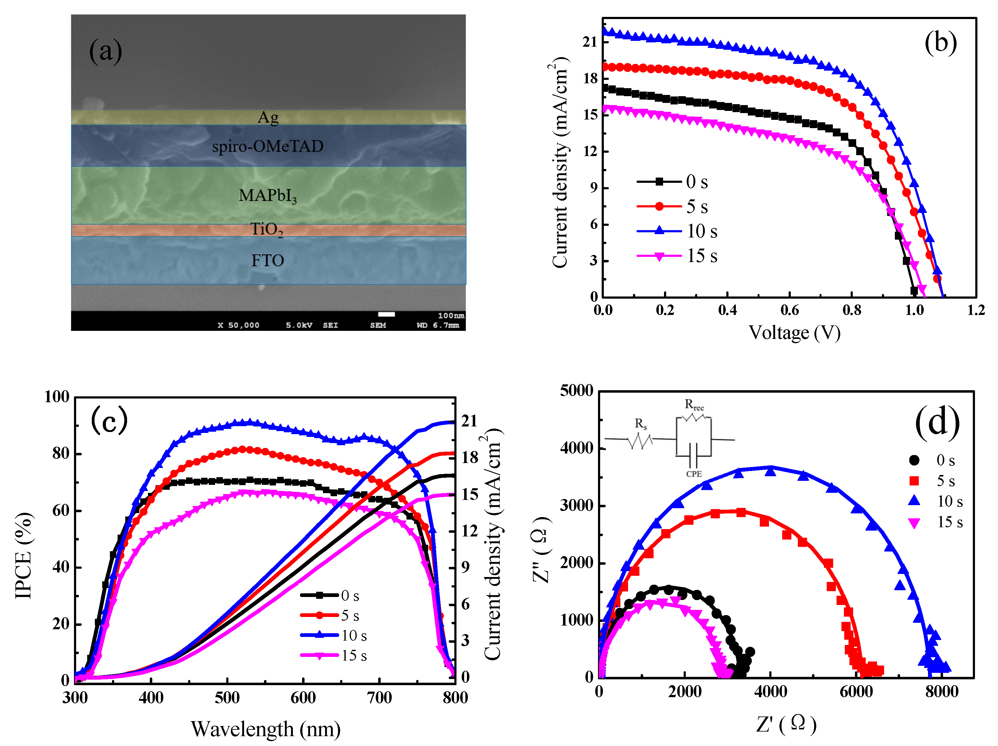
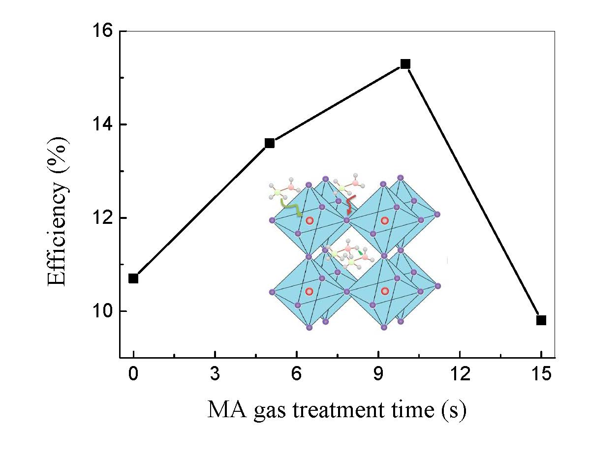
Figure 1. (a) X-ray diffraction (XRD) spectrum and the corresponding; (b) I(110)/I(310) Ratio and the average crystal size of (110) plane of the CH3NH3PbI3 (MAPbI3) films at different CH3NH2 (MA) treatment times; (c) UV–Vis absorption spectra of MAPbI3 films; and (d) photoluminescence (PL) spectrum of FTO/TiO2/MAPbI3 with different times of MA treatment.
Crystals 08 00044 g001
Figure 2. SEM images of MAPbI3 films at different MA treatment times: (a) 0 s, (b) 5 s, (c) 10 s, (d) 15 s, (e) 20 s, (f) 30 s. Tapping-mode AFM height images of perovskite films treated with MA gas at different times: (g) 0 s, (h) 5 s, (i) 10 s.
Crystals 08 00044 g002aCrystals 08 00044 g002b
Figure 3. (a) The cross-sectional view of glass/FTO/TiO2/MAPbI3/spiro-OMeTAD/Ag planar heterojunction perovskite solar cell; (b) J-V curves and (c) incident photon-to-electron conversion efficiency (IPCE) spectra and integrated current density of the perovskite solar cells (PSCs) at different MA treatment times; (d) The impedance spectra of different MA treatment times of PSCs under 0.6 V applied bias in dark, the inset picture is the equivalent circuit.
Crystals 08 00044 g003
Figure 4. The schematic drawing illustrates the process to prepare MAPbI3 polycrystalline film and the setup to vapor treatment process.
Crystals 08 00044 g004
Table 1. Parameters of Current Density-Voltage Measurement and Electrochemical Impendence of the PSCs at different MA treatment times.
Time (s)VOC (V)JSC (mA/cm2)FF (%)PCEave (Best)
(%)
Rs (Ω cm2)Rrec (Ω cm2)
00.99 ± 0.0217.29 ± 0.8359.5 ± 1.710.2 (10.7)5.83265
51.09 ± 0.0119.02 ± 0.6361.3 ± 1.312.5 (13.6)9.56076
101.09 ± 0.0121.85 ± 0.5261.5 ± 1.214.4 (15.3)8.47719
151.02 ± 0.0115.64 ± 0.7654.5 ± 1.68.9 (9.8)4.12876

