
Interplay Effect of Excitation and Temperature on Carrier Transfer between Vertically Aligned InAs/GaAs Quantum Dot Pairs

 , and
, and 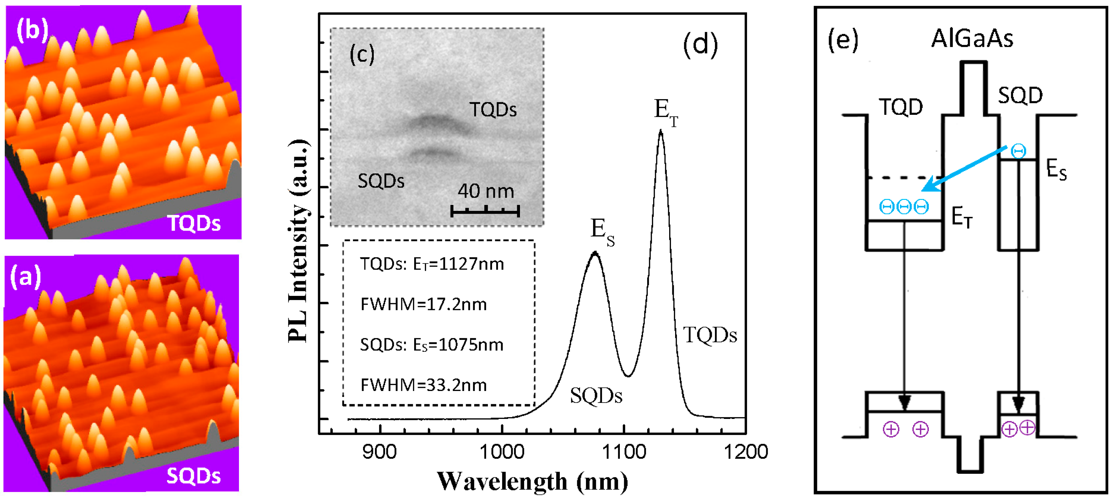
Abstract
:1. Introduction
2. Experiments
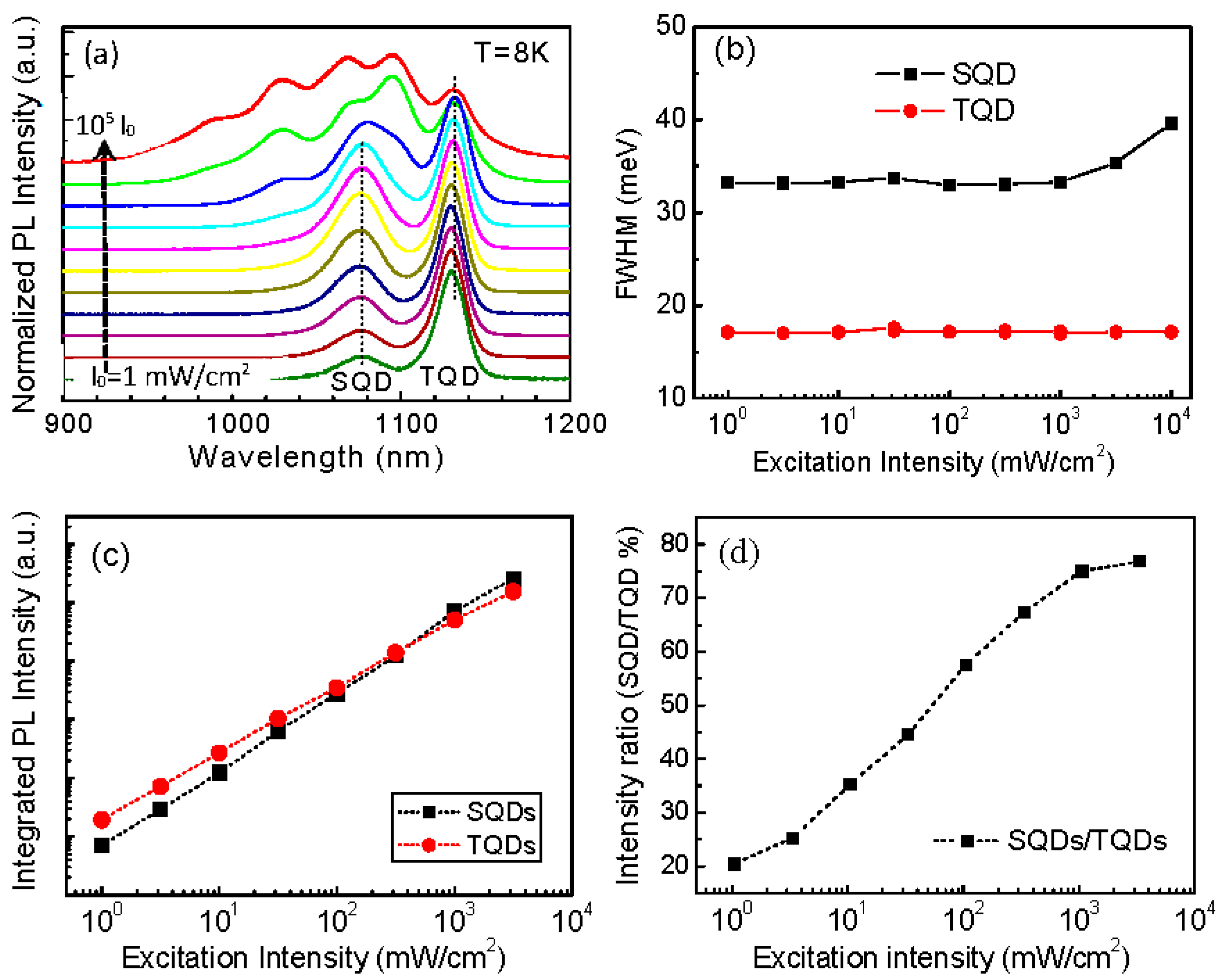
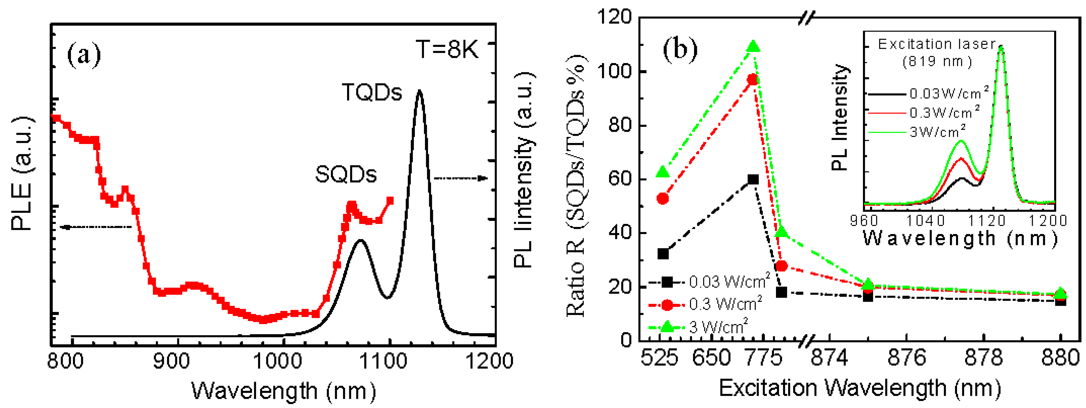
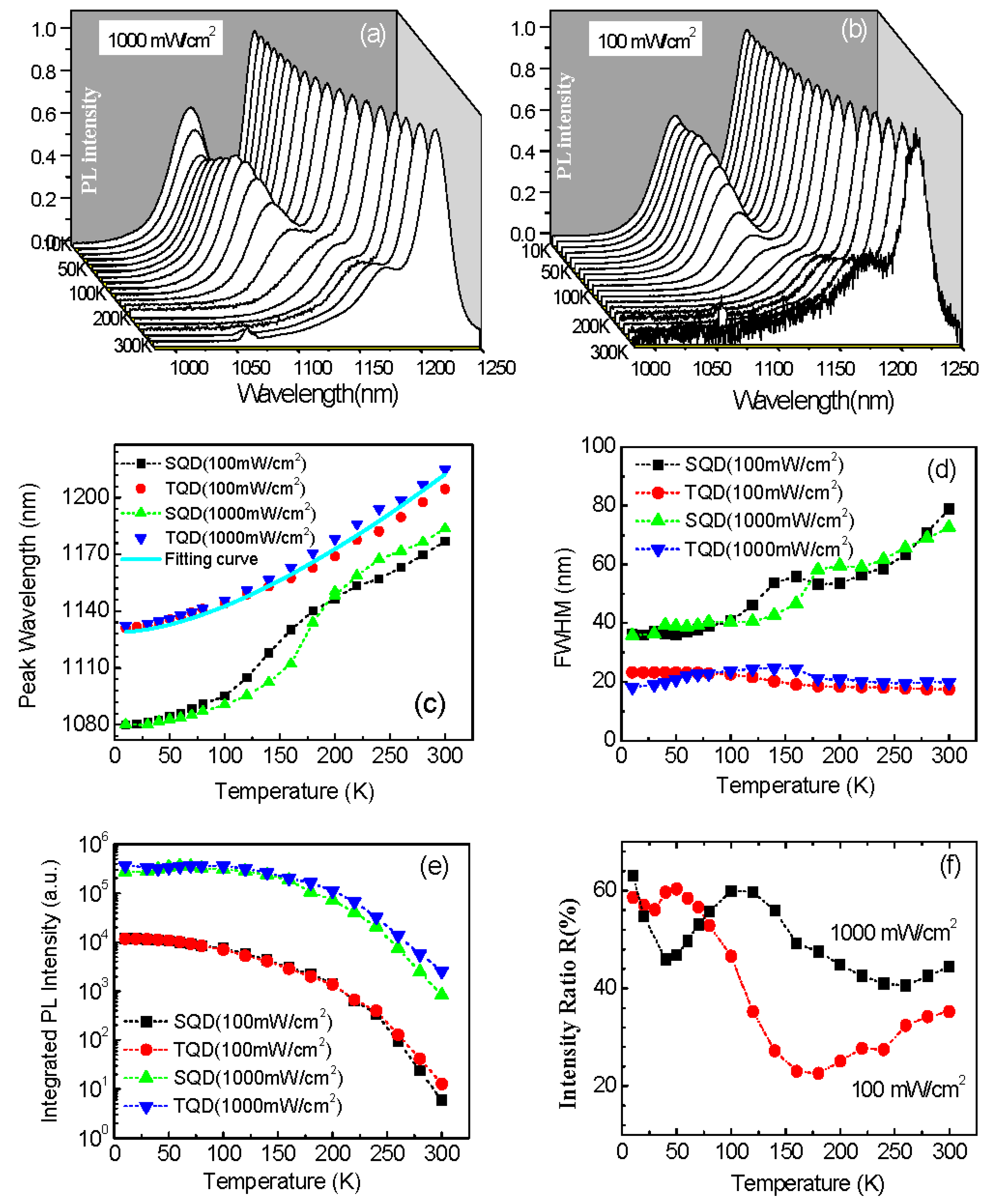
3. Results and Discussion
4. Conclusions
Acknowledgments
Author Contributions
Conflicts of Interest
References
- Bimberg, D.; Grundmann, M.; Ledentsov, N.N. Quantum Dot Heterostructures; Wiley: New York, NY, USA, 1998. [Google Scholar]
- Yuan, Z.L.; Kardynal, B.E.; Stevenson, R.M.; Shields, A.J.; Lobo, C.J.; Cooper, K.; Beattie, N.S.; Ritchie, D.A.; Pepper, M. Electrically driven single-photon source. Science 2002, 295, 102–105. [Google Scholar] [CrossRef] [PubMed]
- Leonard, D.; Pond, K.; Petroff, P.M. Critical layer thickness for self-assembled InAs islands on GaAs. Phys. Rev. B 1994, 50, 11687–11692. [Google Scholar] [CrossRef]
- Nishibayashi, K.; Kawazoe, T.; Ohtsu, M.; Akahane, K.; Yamamoto, N. Observation of interdot energy transfer between InAs quantum dots. Appl. Phys. Lett. 2008, 93, 042101. [Google Scholar] [CrossRef]
- Fry, P.W.; Itskevich, I.E.; Mowbray, D.J.; Skolnick, M.S.; Finley, J.J.; Barker, J.A.; O’Reilly, E.P.; Wilson, L.R.; Larkin, I.A.; Maksym, P.A.; et al. Inverted electron-hole alignment in InAs-GaAs self-assembled quantum dots. Phys. Rev. Lett. 2000, 84, 733–736. [Google Scholar] [CrossRef] [PubMed]
- Bhattacharya, P.; Ghosh, S.; Stiff-Roberts, A.D. Quantum dot opto-eletronic devices. Annu. Rev. Mater. Res. 2004, 34, 1–40. [Google Scholar] [CrossRef]
- Huffaker, D.L.; Park, G.; Zou, Z.; Shchekin, O.B.; Deppe, D.G. 1.3 μm room-temperature GaAs-based quantum-dot laser. Appl. Phys. Lett. 1998, 73, 2564–2566. [Google Scholar] [CrossRef]
- Bailey, C.G.; Forbes, D.V.; Raffaelle, R.P.; Hubbard, S.M. Near 1 V open circuit voltage InAs/GaAs quantum dot solar cells. Appl. Phys. Lett. 2011, 98, 163105. [Google Scholar] [CrossRef]
- Horiguchi, N.; Futatsugi, T.; Nakata, Y.; Yokoyama, N.; Mankad, T.; Petroff, P.M. Quantum dot infrared photodetector using modulation doped InAs self-assembled quantum dots. J. Appl. Phys. 1999, 38, 2559–2561. [Google Scholar] [CrossRef]
- Liu, H.Y.; Wang, T.; Jiang, Q.; Hogg, R.; Tutu, F.; Pozzi, F.; Seeds, A. Long-wavelength InAs/GaAs quantum-dot laser diode monolithically grown on Ge substrate. Nat. Photonics 2011, 5, 416–419. [Google Scholar] [CrossRef]
- Li, X.Q.; Wu, Y.W.; Steel, D.; Gammon, D.; Stievater, T.H.; Katzer, D.S.; Park, D.; Piermarocchi, C.; Sham, L.J. An all-optical quantum gate in a semiconductor quantum dot. Science 2003, 301, 809–811. [Google Scholar] [CrossRef] [PubMed]
- Wu, J.; Hu, X.; Lee, J.; Kim, E.S.; Wang, Z.M. Epitaxially self-assembled quantum dot pairs. Adv. Opt. Mater. 2013, 1, 201–214. [Google Scholar] [CrossRef]
- Fino, N.R.; Camacho, A.S.; Ramírez, H.Y. Coupling effects on photoluminescence of exciton states in asymmetric quantum dot molecules. Nanoscale Res. Lett. 2014, 9, 297. [Google Scholar] [CrossRef] [PubMed]
- Ji, H.M.; Liang, B.L.; Simmonds, P.J.; Juang, B.C.; Yang, T.; Young, R.J.; Huffaker, D.L. Hybrid type-I InAs/GaAs and type-II GaSb/GaAs quantum dot structure with enhanced photoluminescence. Appl. Phys. Lett. 2015, 106, 103104. [Google Scholar] [CrossRef]
- Chakrabarti, S.; Halder, N.; Sengupta, S.; Ghosh, S.; Mishima, T.D.; Stanley, C.R. Vertical ordering and electronic coupling in bilayer nanoscale InAs/GaAs quantum dots separated by a thin spacer layer. Nanotechnology 2008, 19, 505704. [Google Scholar] [CrossRef] [PubMed]
- Mazur, Y.I.; Wang, Z.M.; Tarasov, G.G.; Kunets, V.P.; Salamo, G.J.; Zhuchenko, Z.Y.; Kissel, H. Tailoring of high-temperature photoluminescence in InAs/GaAs bilayer quantum dot structures. J. Appl. Phys. 2005, 98, 053515. [Google Scholar] [CrossRef]
- Bayer, M.; Hawrylak, P.; Hinzer, K.; Fafard, S.; Korkusinski, M.; Wasilewski, Z.R.; Stern, O.; Forchel, A. Coupling and entangling of quantum states in quantum dot molecules. Science 2001, 291, 451–453. [Google Scholar] [CrossRef] [PubMed]
- Tarasov, G.G.; Zhuchenko, Z.Y.; Lisitsa, M.P.; Mazur, Y.I.; Wang, Z.M.; Salamo, G.J.; Warming, T.; Bimberg, D.; Kissel, H. Optical detection of asymmetric quantum-dot molecules in double-layer InAs/GaAs structures. Semiconductors 2006, 40, 79–83. [Google Scholar] [CrossRef]
- Liu, Y.; Liang, B.L.; Guo, Q.L.; Wang, S.F.; Fu, G.S.; Fu, N.; Wang, Z.M.; Mazur, Y.I.; Salamo, G.J. Electronic coupling in nanoscale InAs/GaAs quantum dot pairs separated by a thin Ga(Al)As spacer. Nanoscale Res. Lett. 2015, 10, 271. [Google Scholar] [CrossRef] [PubMed]
- Levi, D.H.; Wake, D.R.; Klein, M.V.; Kumar, S.; Morkoc, H. Density dependence of nonresonant tunneling ln asymmetric coupled quantum wells. Phys. Rev. B 1992, 45, 4274–4279. [Google Scholar] [CrossRef]
- Mazur, Y.I.; Wang, Z.M.; Tarasov, G.G.; Xiao, M.; Salamo, G.J.; Tomm, J.W.; Talalaev, V.; Kissel, H. Interdot carrier transfer in asymmetric bilayer InAs/GaAs quantum dot structures. Appl. Phys. Lett. 2005, 86, 063102. [Google Scholar] [CrossRef]
- Jin, S.R.; Zheng, Y.L.; Li, A.Z. Characterization of photoluminescence intensity and efficiency of free excitons in semiconductor quantum well structures. J. Appl. Phys. 1997, 82, 3870–3873. [Google Scholar] [CrossRef]
- Martini, S.; Quivy, A.A.; Tabata, A.; Leite, J.R. Influence of the temperature and excitation power on the optical properties of InGaAs/GaAs quantum wells grown on vicinal GaAs(001) surfaces. J. Appl. Phys. 2001, 90, 2280–2289. [Google Scholar] [CrossRef]
- Mazur, Y.I.; Dorogan, V.G.; Guzun, D.; Marega, E., Jr.; Salamo, G.J.; Tarasov, G.G.; Govorov, A.O.; Vasa, P.; Lienau, C. Measurement of coherent tunneling between InGaAs quantum wells and InAs quantum dots using photoluminescence spectroscopy. Phys. Rev. B 2010, 82, 155413. [Google Scholar] [CrossRef]
- Shih, C.I.; Lin, C.H.; Lin, S.C.; Lin, T.C.; Sun, K.W.; Voskoboynikov, O.; Lee, C.P.; Suen, Y.W. Effects of crossed states on photoluminescence excitation spectroscopy of InAs quantum dots. Nanoscale Res. Lett. 2011, 6, 409. [Google Scholar] [CrossRef] [PubMed]
- Mazur, Y.I.; Lopes-Oliveira, V.; Souza, L.D.; Lopez-Richard, V.; Teodoro, M.D.; Dorogan, V.G.; Benamara, M.; Wu, J.; Tarasov, G.G.; Marega, J.E.; et al. Carrier transfer in vertically stacked quantum ring-quantum dot chains. J. Appl. Phys. 2015, 117, 154307. [Google Scholar] [CrossRef]
- Chen, J.X.; Markus, A.; Fiore, A.; Oesterle, U.; Stanley, R.P.; Carlin, J.F.; Houdré, R.; Ilegems, M.; Lazzarini, L.; Nasi, L.; et al. Tuning InAs/GaAs quantum dot properties under Stranski–Krastanov growth mode for 1.3 μm applications. J. Appl. Phys. 2002, 91, 6710–6716. [Google Scholar] [CrossRef]
- Sanguinetti, S.; Henini, M.; Grassi Alessi, M.; Capizzi, M.; Frigeri, P.; Franchi, S. Carrier thermal escape and retrapping in self-assembled quantum dots. Phys. Rev. B 1999, 60, 8276–8283. [Google Scholar] [CrossRef]


© 2016 by the authors; licensee MDPI, Basel, Switzerland. This article is an open access article distributed under the terms and conditions of the Creative Commons Attribution (CC-BY) license (http://creativecommons.org/licenses/by/4.0/).
Share and Cite
Liu, Y.; Wang, Y.; Liang, B.; Guo, Q.; Wang, S.; Fu, G.; Mazur, Y.I.; Ware, M.E.; Salamo, G.J. Interplay Effect of Excitation and Temperature on Carrier Transfer between Vertically Aligned InAs/GaAs Quantum Dot Pairs. Crystals 2016, 6, 144. https://doi.org/10.3390/cryst6110144
Liu Y, Wang Y, Liang B, Guo Q, Wang S, Fu G, Mazur YI, Ware ME, Salamo GJ. Interplay Effect of Excitation and Temperature on Carrier Transfer between Vertically Aligned InAs/GaAs Quantum Dot Pairs. Crystals. 2016; 6(11):144. https://doi.org/10.3390/cryst6110144
Chicago/Turabian StyleLiu, Yao, Ying Wang, Baolai Liang, Qinglin Guo, Shufang Wang, Guangsheng Fu, Yuriy I. Mazur, Morgan E. Ware, and Gregory J. Salamo. 2016. "Interplay Effect of Excitation and Temperature on Carrier Transfer between Vertically Aligned InAs/GaAs Quantum Dot Pairs" Crystals 6, no. 11: 144. https://doi.org/10.3390/cryst6110144
APA StyleLiu, Y., Wang, Y., Liang, B., Guo, Q., Wang, S., Fu, G., Mazur, Y. I., Ware, M. E., & Salamo, G. J. (2016). Interplay Effect of Excitation and Temperature on Carrier Transfer between Vertically Aligned InAs/GaAs Quantum Dot Pairs. Crystals, 6(11), 144. https://doi.org/10.3390/cryst6110144