Photonic crystals (PCs) constructed with periodic variations of dielectric permittivity in some specific dimensions are known for their superior feature of photonic band gap (PBG) [
1,
2]. Similar to the characteristic of electronic band gap in semiconductor, photons with wavelengths or frequencies lying in the PBG are forbidden and localized, permitting PCs to hold great promise for applications in a wide range of optical devices [
3,
4,
5,
6,
7]. When a defect layer is inserted in a PC to intentionally interrupt the periodicity, partial defect modes enabling the transmission of photons at specific wavelengths can be obtained within the PBG.
Owing to the unique dielectric and optical anisotropy and sensitive response to external stimuli, liquid crystals (LCs) have received much attention in the past half-century. Since LC phases with periodically helical structures can intrinsically be regarded as PCs, various LC-based PC devices with tunable optical features by light irradiations [
8,
9] or by electric-field treatments [
10,
11] have previously been demonstrated. Alternatively, recent investigations concerning the tunability of defect modes as well as the design of electrically tunable photonic devices have extensively been proposed in the literature by incorporating various types of LCs individually in one-dimensional (1D) multilayer PCs [
12]. Among them, the 1D PC/LC hybrid structures with dynamic-mode LCs allow the wavelength tunability of defect modes in accordance with the electrically controlled birefringence [
13,
14,
15,
16,
17,
18] or polarization-rotation effect [
19]. Along the line of the rapidly emerging concept for green products, several memory-mode LCs as defect layers in PCs have been considered towards the design of energy-efficient devices in that the optical characteristics in the memory state of PC/LC cells persist without the need of any sustaining bias voltage [
20,
21,
22,
23,
24].
In recent years, dual-mode LC cells have widely been studied from the point of view of practical applications because they possess both the dynamic and memory functions in a single device [
25,
26,
27,
28,
29,
30]. Specifically, a dual-mode chiral-agent-doped dual-frequency LC (CD-DFLC) unites the bistable chiral–splay nematic (BCSN) and optically compensated bend (OCB) as the memory and dynamic modes in one cell, respectively [
29]. The DFLC is a LC material whose dielectric anisotropy ∆
ε can be varied by the frequency of the applied electric field [
30]. The DFLC exhibits a characteristic frequency, known as the crossover frequency
fc, to discriminate the sign of ∆
ε. As the frequency is lower than
fc, ∆
ε is positive. In contrast, ∆
ε becomes negative if the applied frequency goes beyond
fc. Based on this mechanism, the CD-DFLC can operate in two optically stable states—the memorable splay and
π-twist states—and in a voltage-sustained state—the dynamic bend state—at frequency of 1 kHz. The switching between the bistable states is achieved by the frequency-revertible dielectric anisotropy of the DFLC together with the electrohydrodynamic flow effect of LC molecules [
30]. In order to make a photonic device that enables not only the electrical tunability but also the multistability in its optical properties, we propose in this work a 1D hybrid photonic structure incorporated with a dual-mode CD-DFLC as the defect layer. The cell configuration, material properties, measurement conditions and methods, and the operation principle of the device are described. Based on the switching mechanism of the CD-DFLC, spectral properties of this hybrid cell operating in the memory mode and dynamic mode are clarified explicitly. The experimental results indicate that the photonic structure revealed in this study can be of use in photonic applications.
The planar-parallel PC cell is composed of a CD-DFCLC defect layer sandwiched between two identical dielectric mirrors. The dielectric multilayer investigated in this work consists of five layers of 68.09-nm-thick Ta
2O
5 with the refractive index
nH = 2.18 and of four layers of 102.37-nm-thick SiO
2 with
nL = 1.47, deposited alternately on an indium–tin-oxide (ITO)-coated soda-lime glass substrate of 1.1 mm in thickness [
12]. The alignment layers were fabricated by spin-coating SE-8793 (Nissan Chemical) on the top surfaces of dielectric multilayers to promote LC’s planar alignment with parallel rubbing directions.
The CD-DFLC having a pitch length of ~22.6 μm was made of the mixture of a DFLC, HEF951800-100 (HCCH), and the chiral agent S-811 (Merck) in proper concentration. Some physical properties of the DFLC at 20 °C are keynoted as follows: The birefringence Δ
n = 0.222 at the wavelength of 589 nm, Δ𝜀 = 2.1 at 1 kHz and Δ𝜀 = −2.02 at 80 kHz. In order to achieve the theoretically equivalent minimizations of free energy in both the splay and
π-twist states for permanent bistability, the thickness of the CD-DFLC layer was fixed at 5 ± 0.5 μm as determined by ball spacers, yielding a well-controlled thickness (
d)-to-pitch (
p) ratio
d/
p around 0.25 [
25].
All the measurements were performed at around 26 °C. The transmission spectra of the hybrid cell were measured with a high-speed fiber-optic spectrometer (Ocean Optics HR2000+, Winter Park, FL, USA) in conjunction with a halogen light source (Ocean Optics HL2000). The frequency-modulated voltage pulses supplied to the cell were generated by a function generator (Tektronix AFG3022B, Beaverton, OR, USA) together with an amplifier (TREK Model 603, Lockport, NY, USA). Note that there is no polarizer employed in the measurements unless explicitly specified.
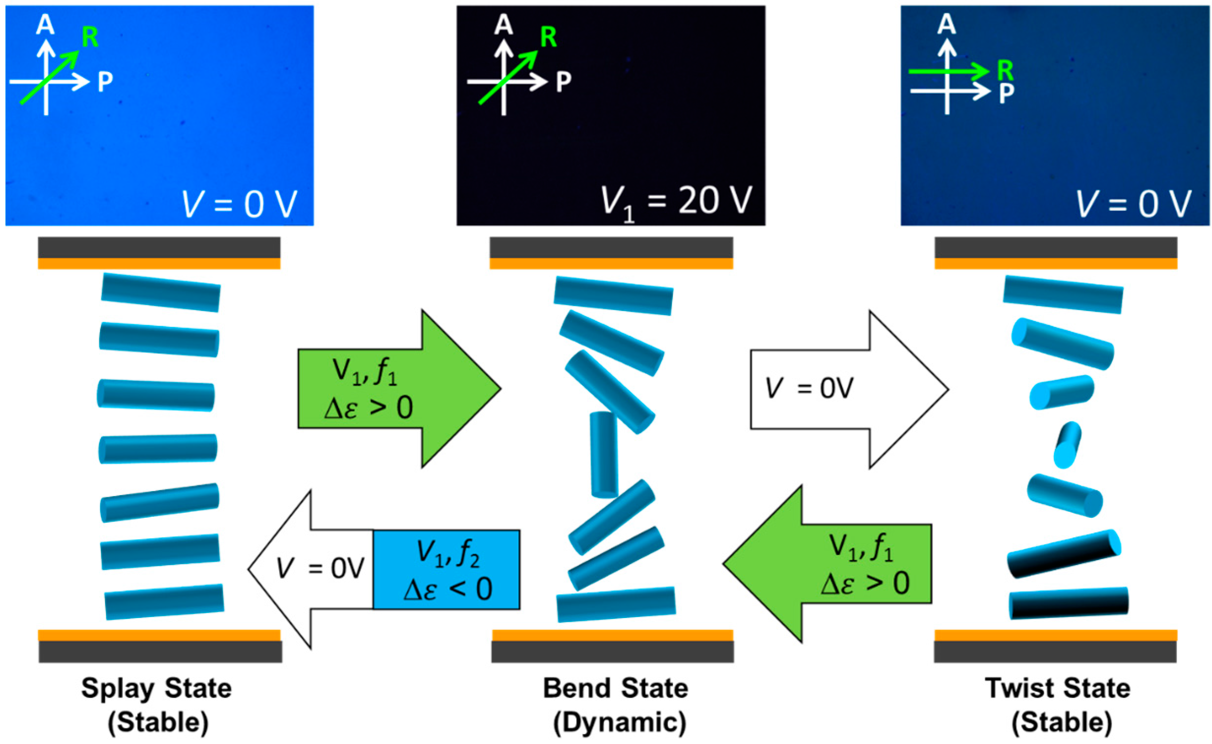
Figure 1 illustrates the state transitions and the corresponding optical textures of the PC/CD-DFLC cell under crossed polarizers [
30]. Here,
f1 and
f2 represent the frequencies fulfilling the criteria of
f1 <
fc and
f2 >
fc, and thus corresponding to the conditions of ∆
ε > 0 and ∆
ε < 0 of the DFLC, respectively.
V1 and
V2 stand for the required amplitudes of voltage pulses for the state transition from the stable splay (sS) state to biased bend (bB) state and the stable twist (sT) state to the bB state, respectively. Consider an initial sS state stabilized in the cell. To determine the difference between the sS and bB states from their appearance by microscopy, the PC/CD-DFCL was set between crossed polarizers with its rubbing direction at an angle of 45° with respect to the transmission axis of one of the polarizers. The bluish appearance in the texture of PC/CD-DFLC in the sS state is dictated by the suppression of light transmission with wavelengths lying in the designated range of the PBG [
20]. When a voltage pulse of
V1 = 10 V at
f1 = 1 kHz is applied to the cell, the LC molecules will intend to be oriented vertically to the cell plane and the sS state will transfer to the bB state through nucleation due to the topological dissimilarity between the splay and bend states. Consequently, the appearance of the optical texture in the bB state becomes dark since most of LC molecules are aligned homeotropically. As the voltage pulse is switched off, the LC molecules will relax from the bB to sT state. The optical texture of the cell in the sT state is colorful, even when the rubbing direction is parallel to the transmission axis of either of the crossed polarizers under the microscope. Note that the sT state is one of the two stable states in the PC/CD-DFLC cell and can be preserved for several months. To carry out the back-switching from the sT to sS state, a voltage pulse of
V1 = 10 V at
f1 = 1 kHz is again applied to the cell to operate the cell in highly tilted bB state. When the driving frequency is switched from
f1 to
f2 instantly in the high-tilt bend state, the LCs will transfer to a transited right-hand twist state through the deformation of reversed twist induced by the backflow effect. In this case, the right-handed twist state is extremely unstable since its elastic free energy is profoundly high compared with those associated with the sS and sT states. The molecules then gradually transit from right-hand twist to the sS state as the applied voltage is switched off. The above-mentioned results indicate that the bistable switching between the sS and sT states is indirect since an intermediate bB state is required. As a consequence, in addition to the switching between the two optically stable states—sS and sT states—for the memory-mode PC/CD-DFLC, the reorientation of LC molecules from the sS state to the highly tilted bB state controlled by applied voltage serves to enable the dynamic mode of the PC/CD-DFLC device in this study.
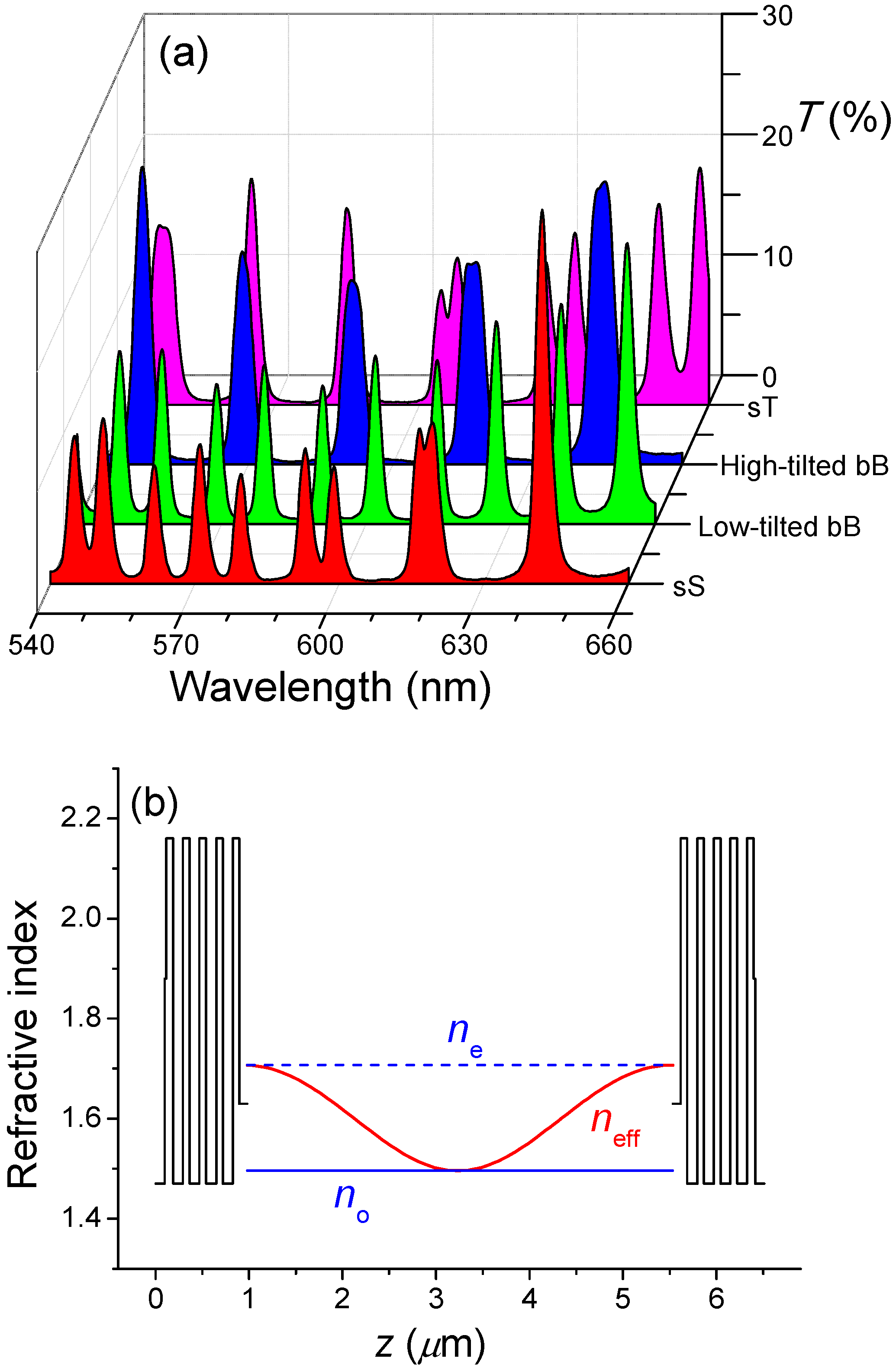
Following the driving scheme established in
Figure 1 for the textual switching,
Figure 2a reveals the transmission spectra of possible textures of the PC/CD-DFLC cell in two stable and two voltage-sustained states. The result demonstrates that distinct spectral profiles of the defect modes corresponding to the four switchable states in the PC/CD-DFLC can be obtained due to the different contributions of the ordinary (
no) and extraordinary (
ne) refractive indices to the overall effective refractive index (
neff) in these states. The values of
neff in the sS, sT and low-tilted bB states are contributed by both
no and
ne, whereas
neff in the high-tilted bB state (i.e., the homeotropic state) is dictated solely by
no (
Figure 2b). Accordingly, the transmission profile of the defect modes in the high-tilted bB state exhibits “fewer” defect-mode peaks and plainer spectrum in comparison with those in the other states. Referring to the feature of dual-mode operation of the CD-DFLC, in the following, we firstly investigate the spectral characteristics of the two memorable states (i.e., the sS and the sT states) of the hybrid PC cell. Moreover, the spectral profiles of defect modes, attributable to the components of the ordinary and extraordinary refractive indices, can further be resolved by placing a polarizer between the light source and the cell with its transmission axis perpendicular and parallel to the rubbing direction of the cell, respectively. The discussion on the electrical tuning of the defect-mode wavelengths for two orthogonal polarization states of light are further demonstrated by operating the cell in the dynamic mode.
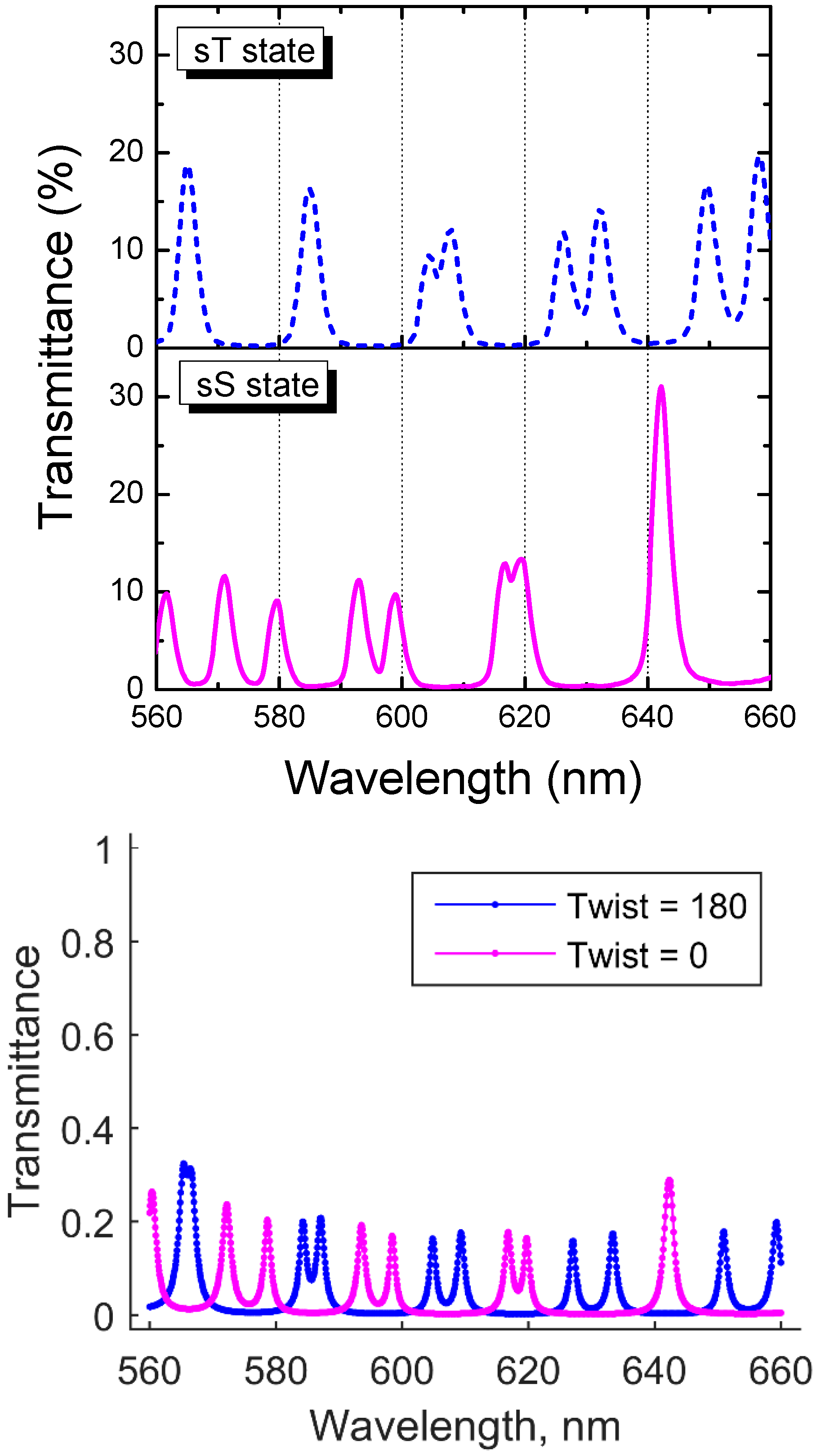
Figure 3 displays partial defect modes in the spectrum, ranging from 560 to 660 nm, of the two stable states in the PC/CD-DFLC cell. In the case of the stable sS state, all molecules are virtually oriented identically with an average axis parallel to the rubbing direction. The spectral profile of a defect mode for the unpolarized light thus contains two peaks due to the contribution of both the
ne and
no components to the optical path length. Note that the resolution as well as the transmission of these two peaks depends on the vector sum of the ordinary and extraordinary refractive indices. When the electrical switching takes place from the sS to the sT state, the shift in wavelength of defect-mode peaks results from the additional polarization rotation of light, dictated by the adiabatic following effect. Because the sT state shows 180°-twisted molecular structure with axis perpendicular to the substrate plane, the phase difference between the sS and the sT states is expected to be π. Accordingly, it can clearly be recognized from
Figure 3 that the wavelength regimes involving the peaks of defect modes in the sS (sT) state overlap with the stop bands in the sT (sS) state, indicating the complementary nature in transmission wavelengths. For instance, in the wavelength range between 590 and 600 nm, a defect mode with two intense peaks is obtained in the sT state but it is suppressed (with transmission approaching to zero) when switching the cell to the sS state. Specifically, these two discriminable sets of defect modes obtained in the sS and sT states persist permanently without any applied voltage. This indicates that the PC/CD-DFLC cell operating in the memory mode is applicable for the design of multichannel wavelength filters with the concept of low power consumption owing to the memorable defect modes in either stable state. In comparison with previously reported hybrid PC devices with various chiral-agent-doped LCs, it has been shown in the PC/twisted-nematic-LC cell that the spectral properties of defect modes are dominated primarily by the adiabatic following effect when the phase retardation is larger than the Gooch–Tarry first minimum condition [
19]. Moreover, using cholesteric LC with a helical pitch much shorter than the cell gap as the defect layer, each resultant defect mode in the spectrum of the PC/cholesteric-LC cell exhibits a single peak for the unpolarized light in that the effective refractive index becomes (
ne +
no)/2 for all polarization directions of light [
22,
23]. To verify the observed results from the experimental spectra, sophisticated simulations, which take the optical extinction and dispersion into account, were carried out using MATLAB as comparatively shown in the bottom panel of
Figure 3. Firstly, the orientational structure within the cell was calculated by means of the energy minimization of elastic deformations of the director field [
31]. Then, by applying the Berreman 4 × 4-matrix method [
32], the light transmission was simulated. Note that the numerical value of the cell gap has been reasonably tuned to 4.555 μm and the simulated data (bottom panel) are in satisfactorily good agreement with the laboratory spectra (top panel) except a noticeable discrepancy at 585 nm. It is likely that the simulated peak splitting at this wavelength in the
π-twist state was hidden by spectral broadening in the experimental measurement.
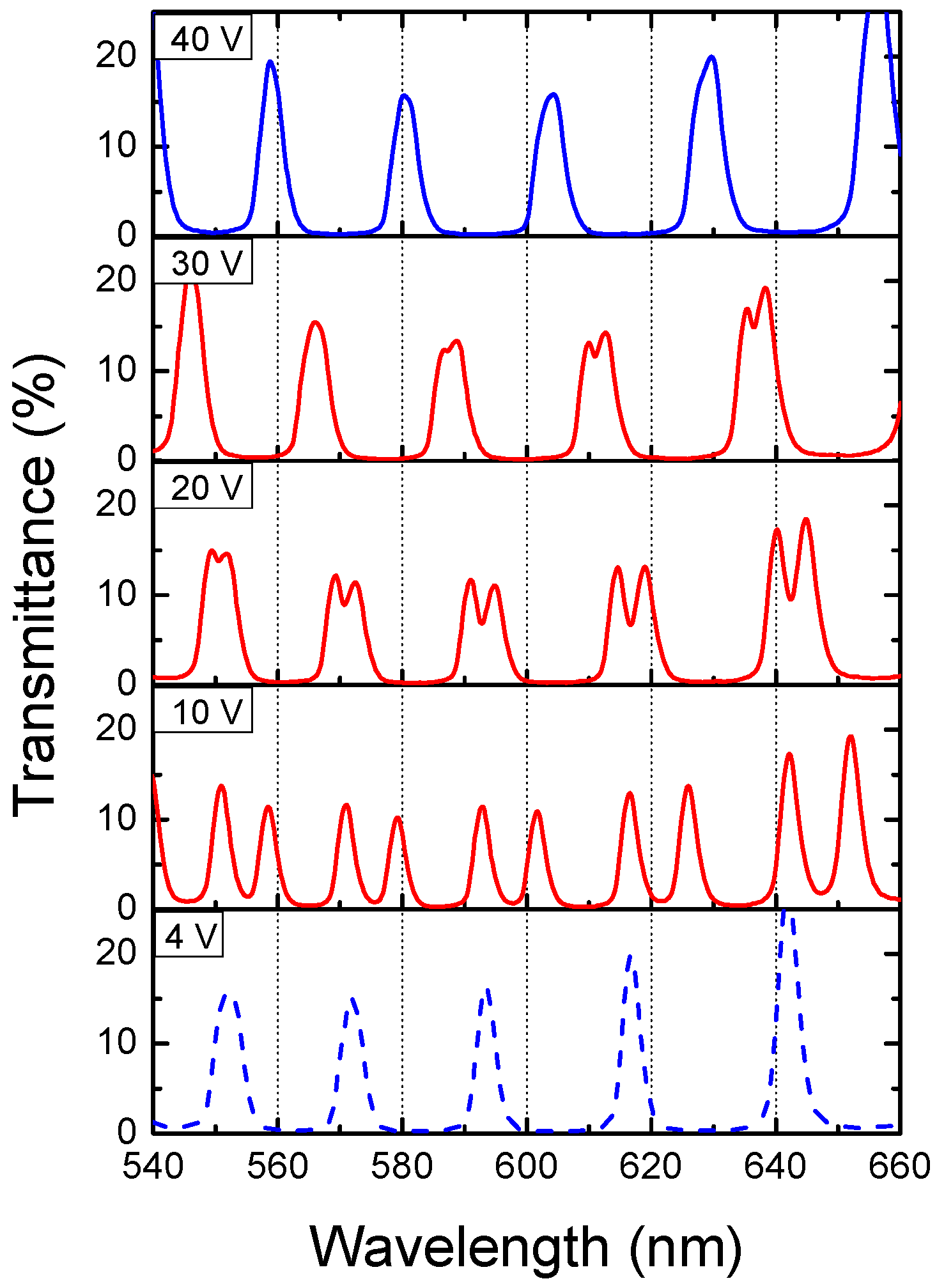
Considering the optical properties of the dynamic mode of PC/CD-DFLC,
Figure 4 depicts the transmission spectra of the cell under the application of voltage pulses with variously given amplitudes at frequency of 1 kHz. Here, the initial state is the sS state. In the case of
V = 4 V where the LC molecules are reoriented to the transited splay state, the resulting transmission in each defect mode is attributable to the superposition of the ordinary and extraordinary components, originating from the vector sum of the ordinary and extraordinary refractive indices. As the applied voltage is increased from
V = 4 V to
V = 40 V to impose the state transition from the sS to high-tilted bB state, one can observe the recombination of defect-mode peaks as a function of increasing voltage due to the variation in
neff. To make clearly the tuning on the ordinary and extraordinary defect modes by applied voltage, the voltage dependence of wavelengths of some specific defect modes was measured with a linear polarizer inserted between the light source and the cell, as shown in
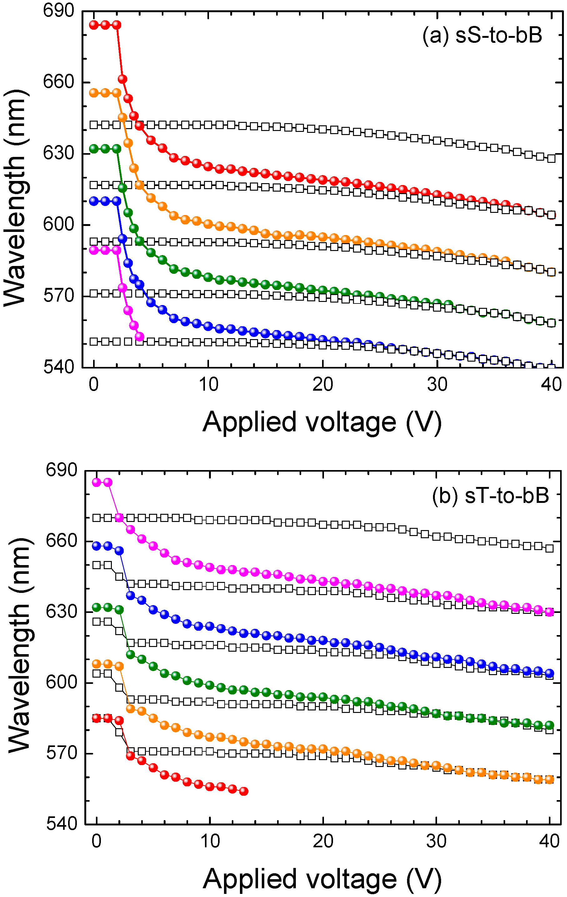
Figure 5. The E-mode and O-mode represent the extraordinary and ordinary defect modes, measured by setting the transmission axis of the polarizer parallel and perpendicular to the rubbing direction of the cell, respectively. Firstly, the cell is considered to be initially stabilized in sS state. In the E-mode case as shown in
Figure 5a, blue shift of defect modes is realized with increasing voltage because of the voltage-induced reorientation of LC molecules from the sS to the bB states and thus the decreased effective refractive index from
ne to
no. This result is in good agreement with that of the PC/planar-aligned LC structure which is attributable to the mechanism of the electrically controlled birefringence of dynamic mode LCs [
13]. The range for wavelength tuning through the sS-to-bB transition in the PC/CD-DFLC is 75 nm with applied voltage of
V = 40 V. On the other hand, the defect-mode peaks in the O-mode (
Figure 5a) do not in principle remain constant, either, but rather shift to shorter wavelength when the applied voltage is higher than 25 V. Referring to our previous research [
24], it is suggested that the blue shift of the ordinary defect modes results from the reduction of the optical path length, caused by the field-induced substrate distortion in the central region or compression of the cell. Similarly, results shown in
Figure 5b indicate that electrical tunability in the E-component of defect modes can also be realized, via the continuous change of molecular orientation from the stable sT state to the bB state with increasing voltages. Notably, the wavelength variation of the O-component defect modes for the sT-to-bB transition at voltages lower than 3 V is greater than that for the sS-to-bB transition, presumably due to the incomplete adiabatic following of light in the 180°-twisted sT state. The tunable wavelength for the E-component defect modes (~54 nm) by the sT-to-bB transition is somewhat narrower than that by the sS-to-bB transition. Because the 180°-twisted state is known to be the transient state during the textural transition from the bend to the splay state, this can reasonably be explained by the smaller voltage-induced phase changes in the sT-to-bB transition. Note that other 1D PC hybrid cells containing memory-mode LCs have been reported to possess wavelength tunability, too, when bistable chiral homeotropic nematic (BHN) [
20] and dual-frequency cholesteric liquid crystal (DFCLC) [
22,
23] are infiltrated as the central defect layers. However, since the tunability is realized by electrical switching from the tilted-twist to homeotropic state in PC/BHN and from scattering focal-conic to planar or homeotropic state in PC/DFCLC, the tunable range in wavelength of these two hybrids is limited due to the limited variation in
neff.
In conclusion, we have demonstrated a unique hybrid structure comprising a 1D PC and a dual-mode CD-DFLC as the central defect layer. The spectral properties of this 1D PC/CD-DFLC hybrid structure in four distinct states have been investigated. Our results show that the transmission profiles of the defect modes are memorable and electrically tunable when operating in the memory and dynamic modes, respectively. Owing to the full-range variation in neff from sole ne to no, the tunable range of a defect-mode wavelength in our proposed cell is not only comparable to those in hybrid PC cells comprising dynamic-mode LCs but is superior to those in cells with memory-mode LCs. Consequently, the integration of memorable and tunable properties in one device paves a new pathway for its potential applications in optical devices such as energy-saving waveguides, cavities, mirrors, optical switches, multichannel filters and wave-division multiplexers.


