Review

Morphological and Structural Control of Organic Monolayer Colloidal Crystal Based on Plasma Etching and Its Application in Fabrication of Ordered Gold Nanostructured Arrays

Key Lab of Materials Physics, Anhui Key Lab of Nanomaterials and Nanotechnology, Institute of Solid State Physics, Cihnese Academy of Sciences, Hefei 230031, China
*
Author to whom correspondence should be addressed.
Crystals 2016, 6(10), 126; https://doi.org/10.3390/cryst6100126
Submission received: 9 June 2016 / Revised: 22 August 2016 / Accepted: 18 September 2016 / Published: 26 September 2016
(This article belongs to the Special Issue Colloidal Crystals)

Abstract

:
The organic monolayer colloidal crystals, which are usually prepared by self-assembling, could be used as templates, due to their interstitial geometry, for the periodically arranged nanostructured arrays, which have important applications in many fields, such as photonic crystals, information storage, super-hydrophobicity, biological and chemical sensing. Obviously, the structures of the obtained arrays mainly depend on those of the templates. However, the self-assembled monolayer colloidal crystal is exclusive in structure and for its hexagonal close-packed colloidal arrangement, leading to the limitation of the monolayer colloidal crystal as the template for the nanostructured arrays. Therefore, structural diversity is important in order for colloidal crystals to be used as the templates for various nanostructured arrays. Recently, there have been some reports on the morphological and structural manipulation of the organic monolayer colloidal crystals. In this review article, we focus on the recent progress in morphological and structural manipulation of polystyrene monolayer colloidal crystals based on plasma etching, and its application in the fabrication of the ordered gold nanostructured arrays with different structures, mainly including close-packed monolayer colloidal crystal and its transferrable property; structural manipulation based on plasma etching; and fabrication of gold nanostructured arrays based on varied monolayer colloidal crystals as template.

1. Introduction

Periodically arranged nanostructured arrays are an important basis of next-generation devices and have potential applications in fields such as optics [1], electronics [2], optoelectronics [3], information storage [4], super-hydrophobicity [5], biological and chemical sensing [6], and surface-enhanced Raman scattering (SERS)-based devices [7,8,9]. Thus far, there have been many methods developed to fabricate these arrays, including aluminum oxide (AAO) template technique [10,11], nano-imprint lithography [12], electron beam ligthography [13] and colloidal lithography [14,15,16], etc. Among these, colloidal lithography is an inexpensive, flexible, and efficient method for fabrication of periodically arranged nanostructured arrays on a large scale by using the mono-, or bi-layer organic colloidal crystals as templates, due to their interstitial geometry. The organic monolayer colloidal crystals are usually prepared based on the principle of colloidal self-assembly [17,18,19,20,21,22,23,24]. There have been many routes developed to fabricate the colloidal crystals by self-assembling, such as the spin-coating method [21], dip-coating method [22] and gas/liquid interface self-assembly [23,24].
However, through the above routes, the obtained monolayer colloidal crystal has a unique structure and a hexagonal close-packed colloidal arrangement, leading to the application limitation of the monolayer colloidal crystal as the template for the nanostructured arrays. Therefore, structural diversity of the organic colloidal crystals is very important in order for them to be used as templates for various nanostructured arrays. Recently, there have been some reports on the morphological and structural manipulation of the organic monolayer colloidal crystals. Here, we focus on the recent progress in morphological and structural manipulation of polystyrene (PS) monolayer colloidal crystal based on plasma etching and its application in the fabrication of the ordered gold nanostructured arrays with different structures, mainly including the close-packed monolayer colloidal crystal and its transferrable property, structural manipulation based on plasma etching, and fabrication of gold nanostructured arrays based on varied monolayer colloidal crystals as templates.

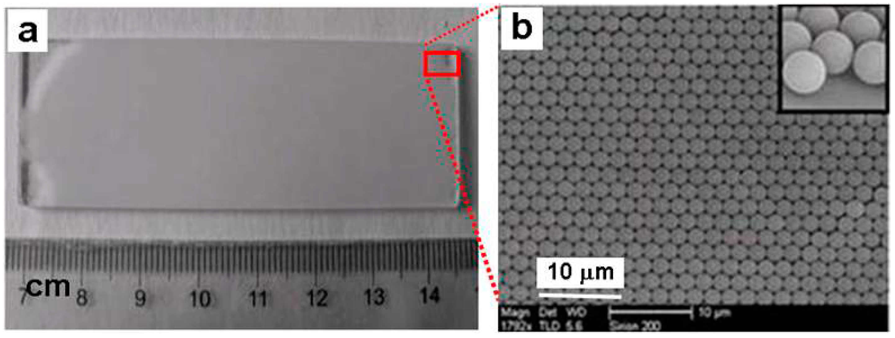
2. Close-Packed Polystyrene (PS) Monolayer Colloidal Crystal and Its Transferrable Property

For fabrication of the close-packed PS monolayer colloidal crystal via self-assembling, ordinary glass slide substrates with a certain size should be firstly washed with acetone, ethanol, and distilled water in an ultrasonic bath, and sequentially cleaned with piranha solution (98% H2SO4/H2O2 3:1), a H2O/H2O2/NH4OH 5:1:1 solution and distilled water [25]. The suspension of the PS spheres with a certain size is then dropped on the cleaned glass slide for self-assembling at the air-water interface [23]. Large-area-ordered PS colloidal monolayers would thus be formed on the slide. Figure 1 shows the typical PS colloidal monolayer with 2 μm in the PS sphere’s diameter on the glass. The PS spheres are close-packed and hexagonally arranged with monolayer and periodical interstitial geometry.
Further, due to the surface tension of the water or aqueous solution and the difference in the wettability between the glass substrate and the PS monolayer colloidal crystals, if we put the glass slide with the PS colloidal monolayer into water in a cup, the monolayer could be stripped off from the glass and float to the surface of the water [21]. Thus the as-prepared PS colloidal monolayer could have a good transferability and be transferred from the glass to any other desired substrates including silicon, silica, mica, copper grid in transmission electron microscope (TEM), and even the other hydrophobic and curved surfaces. Figure 2 gives an example of such transferability from a flat glass to another substrate. First, an as-prepared PS colloidal monolayer on a glass slide is slowly placed, on a slant, into a cup of distilled water (see Figure 2a). Then the monolayer is peeled off from the glass due to the surface tension of water, and floats on the water surface with good integrity (Figure 2b). Finally, the monolayer on the water surface is picked up with a desired substrate (a silicon wafer in this figure) (Figure 2c,d). After drying, the monolayer is transferred on a new substrate. This transferability greatly extends the application of the colloidal crystals as the template since it could be used for the fabrication of micro/nanostructure arrays on any desired substrates.

3. Structural Manipulation Based on Plasma Etching

As mentioned above, the self-assembly-induced colloidal monolayers are close-packed. Obviously, for their applications as templates, non-close-packed colloidal monolayers with different structural parameters, including the spacings between the adjacent PS spheres, are important to fabricate the various nanostructured arrays. Recently, some techniques have been developed to prepare the non-close-packed colloidal monolayer with the controlled interstitial spaces among the adjacent colloidal spheres. For example, Ren et al. [26] fabricated the non-close-packed colloidal monolayer through coupling lift-up soft lithography and solvent-swelling of polydimethylsiloxane (PDMS). Jiang et al. [27] reported a changed spin-coating technique for the production of monolayer non-close-packed colloidal crystals. Generally, using these routes, the distance between the centers of adjacent colloidal spheres can only be adjusted in a very small range. Accurate control of the spacings between the adjacent colloidal spheres, in accordance with our needs, is still a challenge. Recently, our group developed a very simple method for fabrication of the non-close-packed PS colloidal monolayer based on plasma etching of the corresponding close-packed PS monolayer colloidal crystals [28].

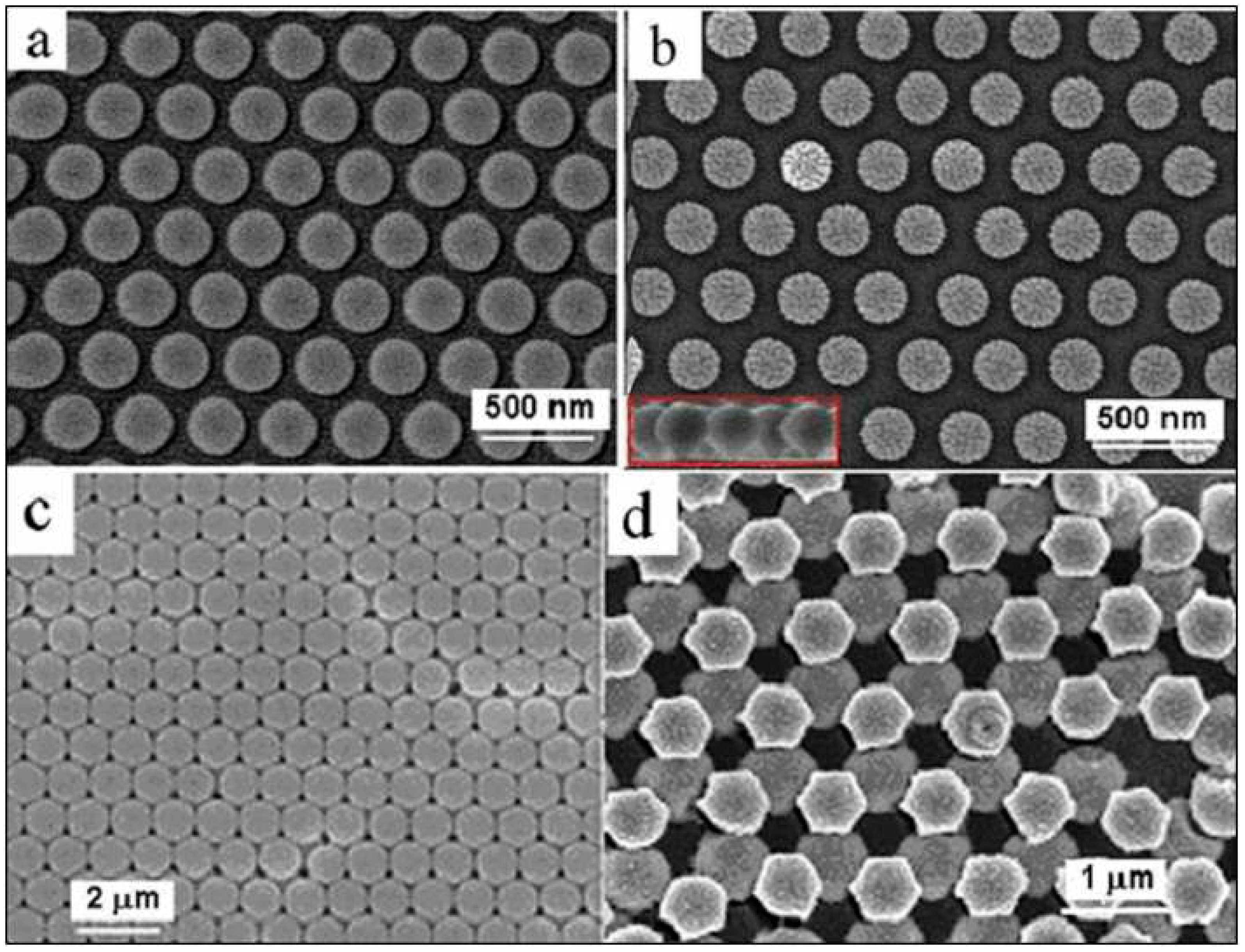
3.1. Etching of the As-Prepared Close-Packed Colloidal Monolayer

Plasma etching technology is an ordinary technique in the field of semiconductor, and usually used to etch silicon and some organic materials. Generally, SF6, O2 and Ar are used as the reactive gases. Plasma bombardment can produce an isotropic etching process, and induce size’s reduction of the PS spheres on the substrate but keep the hexagonally arranged structure of the PS’s spheres. Typically, Ar+ ions were used as the plasma etching gas, and the original monolayer colloidal crystal with hexagonal close-packed PS spheres, as illustrated in Figure 1, was etched in a plasma etching instrument (PDC-32G-2) at a pressure of 0.2 mbar and a input power of 100 W. After etching for a certain time, the hexagonal close-packed structure can be turned into a non-closed monolayer colloidal crystal. Figure 3a,b shows the scanning elelctron microscopic (SEM) images of the etched PS colloidal crystal, corresponding to the as-prepared monolayer with initial size 350 nm in PS sphere diameter after etching for 5 min and 9 min respectively. With increasing the etching time, the size of the PS spheres decreased but the etched PS spheres are still spherical and hexagonally arranged, as illustrated in Figure 3b and its inset. Obviously, the spacing between the etched PS spheres depends on the etching parameters. Under a given power, the longer etching induces the bigger spacings and the smaller etched PS spheres. Also, for the close-packed double-layer colloidal crystals, we can also obtain the non-close-packed double-layer colloidal crystal by the Ar+ plasma etching, as typically illustrated in Figure 3c,d.
It should be mentioned that the PS spheres cannot be reduced in size unlimitedly by etching. When the PS spheres are etched to a small enough size, such etched PS spheres on the substrate could be unstable and may move nearby during further Ar+ plasma etching due to the too-small mass (the airflow and etching are not uniform absolutely). It means that there exists the largest interstitial distance between the adjacent etched PS spheres or the lowest etched PS particle surface fraction achievable by etching an as-prepared close-packed PS colloidal monolayer, which depends on the initial PS sphere’s size and the etching conditions. In our experimental conditions, only when the size is larger than about 100 nm, are the PS spheres, which are point-contact with the substrate, robust to etching. Otherwise, the PS spheres on the Si wafer are unstable and some of them would move nearby during etching. Typically, Figure 4a,b shows the PS colloidal monolayer, with 200 nm in initial PS sphere’s diameter, after etching 6 min and 7 min (100 W in power). After etching for 6 min, the PS spheres were reduced to 115 nm but still immobilized (Figure 4a). If further etching, however, some of the etched PS spheres were unstable and move nearby (Figure 4b).
Further, if the above etched PS colloidal monolayer is heated, the etched PS spheres would adhere to the substrate strongly enough to be further etched. Therefore, if subsequently alternating between heating and etching, we could obtain a much lower etched PS particle surface fraction or a much larger interstitial distance between the adjacent etched PS spheres. Figure 4c shows the results after alternately heating (at 120 °C for few seconds) and etching several times the as-prepared PS colloidal monolayer with 120 nm in initial PS sphere diameter. The PS spheres were reduced from 120 nm to about 15 nm in size and still immobilized. If we carefully control the heating and etching conditions, the lower PS particle surface fraction or the larger interstitial distance could be achieved.

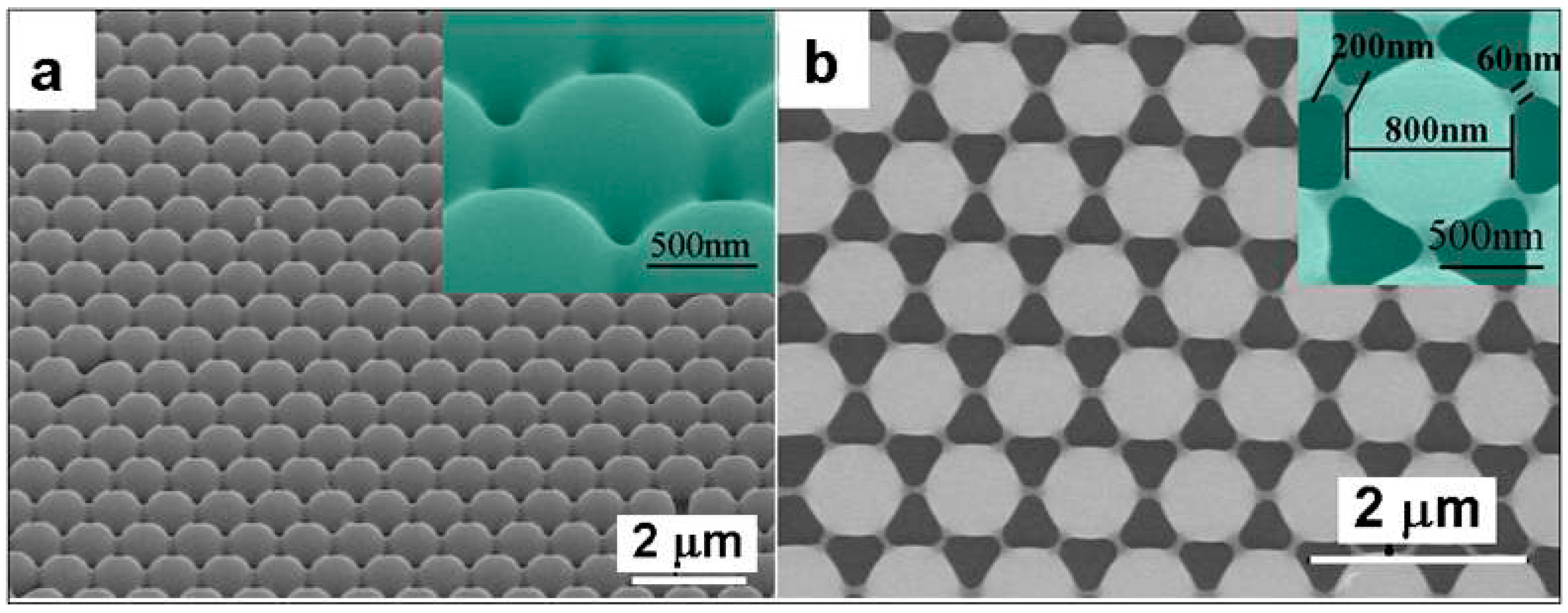
3.2. Etching of the Heated Close-Packed Colloidal Monolayer

The glass-transition point of PS spheres is about 110 °C. Appropriate heating treatment at or above 110 °C can modify the morphology and structure of the as-prepared PS colloidal monolayer on a substrate. For such a heated close-packed colloidal monolayer, the etching would induce different morphological evolution from that mentioned above. Typically, a hexagonally close-packed PS colloidal monolayer of 1 μm PS sphere diameter was transferred onto an expected substrate, as shown in Figure 2, and then heated at 120 °C for 2.5 min. The adjacent PS colloidal spheres become planar-contact and all PS spheres contact the substrate with a certain area, instead of the original point-contact due to the heating-induced sintering process, as illustrated in Figure 5a. All PS spheres are symmetrically deformed. After the Ar+ plasma etching for 10 min, the heated or deformed PS spheres in the monolayer were reduced in size, thus appearing spherical, and the monolayer became non-close-packed, in which the etched PS spheres linked with each other by a short-bar or each etched PS sphere is surrounded by six linking-bars (see Figure 5b). Such an etched PS colloidal monolayer is actually dualistic in configuration, or consists of the hexagonally arranged etched PS spheres and six linking-bars surrounding each of them. Due to the isotropic etching induced by Ar+ plasma bombardment, the heated PS spheres were reduced symmetrically in size, and the contact area between the adjacent PS spheres was also reduced to form a short-bar, which links the adjacent etched PS spheres.
When further etching, the short bars between two adjacent PS spheres shown in Figure 5b would become thinner and thinner, and about 2 min later, break down at the middle of the short bars, leaving six protuberances around each PS sphere symmetrically. From the top view, the hexagonal PS objects were formed and non-closely arranged, as shown in Figure 6. We can control the period by selecting PS spheres with different diameters. By such heating and etching, we can increase the structural diversity of the PS colloidal monolayers as templates, which is of importance to the fabrication of the ordered arrays with different structures.

4. Fabrication of Gold Nanostructured Arrays

Due to the interstitial geometry in the PS monolayer colloidal crystals, by using them as the template or mask and depositing some materials into the interstitials of the template, we can fabricate the nanostructured arrays with various structural parameters, such as nanohole arrays [30], nanoplate arrays [8], nanorod arrays [31], etc., depending on the deposition routes. As for removal of the PS template, it is easily dissolved by immersion into the methylene chloride (CH2Cl2) solution and removed completely by subsequently cleaning. Here, we only introduce the fabrication of three kinds of gold nanostructured arrays: the triangular nanoplate arrays, the opening-nanoshell arrays and the binary-structure arrays, using the close and non-close-packed PS monolayer colloidal crystals as templates.

4.1. Triangular Nanoplate Arrays from the Close-Packed Monolayer Colloidal Template

For the monolayer colloidal crystals with hexagonal close-packed structure, one triangular interstitial (from top view) exists among three adjacent PS spheres contacted with each other. If using electrochemical deposition or sputtering (or evaporation) deposition methods in vertical growth mode, [32,33], the triangular nanoplates can be formed due to the interstitial geometry of the PS colloidal monolayer. For instance, after the hexagonal close-packed PS monolayer colloidal crystal was heated at 120 °C for a certain time to make the adjacent PS colloidal spheres become planar-contact instead of the original point-contact, we could fabricate gold nanoplate arrays with controllable or different spacings between the adjacent nanoplates by evaporation or sputtering deposition method in vertical growth mode. Typically, Figure 7 shows the triangular gold nanoplate arrays with different spacings by sputtering deposition of Au on the hexagonal close-packed PS colloidal monolayers pre-heated at 120 °C for different durations and removing the PS spheres. With the heating time increasing, the contact areas among the adjacent PS spheres and between the PS spheres and substrate, increase. Correspondingly, the triangular interstitial spaces (from top view) diminish. The size of triangular nanoplates therefore decreases and the spacing between the adjacent nanoplates increases with the heating time (Figure 7). We can thus control the spacings and size of the nanoplates.

4.2. Opening-Nanoshell Arrays from Non-Close-Packed Monolayer Colloidal Crystals

Further, if using as the template the non-close-packed colloidal monolayer with different spacings (Figure 3) we can fabricate the gold opening nanoshell-ordered arrays with different spacings and/or shell thicknesses. Typically, a thin gold layer was deposited on the etched PS colloidal monolayer via sputtering deposition at a rate of 6 nm min−1 in thickness. The thickness of gold layer was controlled by the sputtering deposition time. The colloidal monolayer coated with the gold thin-layer was immersed in CH2Cl2 solution for 10 min to dissolve the PS spheres, and a Au nano-hell array was left after cleaning with distilled water several times and drying with high-purity flowing nitrogen [34], as shown in Figure 8. Figure 8a shows a SEM image of the as-prepared array, after sputtering deposition of Au on the etched PS colloidal monolayer (with 200 nm in the initial PS sphere’s size), for 24 s (2.4 nm in deposition thickness) and removal of PS spheres. It exhibits a hexagonal non-close-packed nanoshell array. The gaps or spacings between the adjacent nanoshells in the array are about 15 nm, and there were six symmetrical gaps around each nanoshell, as shown in Figure 8b. The number density of the gaps is about 1010/cm2. The density can be controlled by the initial size of PS spheres in the template. Figure 8c gives the corresponding TEM image of the nanoshell array after scraping from the substrate. It still keeps its hexagonal non-close-packed arrangement. The inset is the corresponding fast Fourier transform (FFT), and the diffraction pattern should originate from the periodical structure of the Au array, which indicates the hexagonal-packed structure. Meanwhile, from the TEM image of the slightly slantwise array, we can clearly identify the shell structure of each unit or block, according to the thick brim and the thin midst, as shown in Figure 8d. Moreover, each unit in the array is an incomplete hollow sphere with a “placket” at the bottom. We thus refer to it as an opening-shell structure. This is attributed to non-shadow-deposition on the etched PS spheres under sputtering deposition [34].
Such an array exhibited tunable surface plasmon resonance (SPR) with the shell thickness. Figure 9 shows the optical absorption spectra for the Au opening-shell arrays with different shell thicknesses (from 2 nm to 9 nm, estimated according to the deposition rate of 6 nm/min). There exists a local SPR peak around 750 nm for the array with 2 nm in shell thickness, which red-shifts to 1525 nm with increase of the shell thickness to 9 nm. Such shell thickness-dependent SPR is different from the previous reports [35,36] for the isolated Au shells (or hollow particles), which showed the SPR shifting to short wavelength with increasing shell thickness. Here the SPR should not mainly originate from a single Au opening-nanoshell, but from the electromagnetic plasmonic coupling of the adjacent Au opening-shells. The coupling effect of the local surface plasmon among the adjacent opening-nanoshells can enhance electromagnetic fields at the nano-gap sites [37,38]. The red-shifting of the SPR peak should be attributed to the decreasing spacings between adjacent nano-units [34]. As for the broadening and asymmetry of the SPR peaks in Figure 9, it could be mainly attributed to dispersivity in structural parameter of the nanoshell arrays.
It should be mentioned that the optical absorption spectra of the Au-nanostructured arrays are associated with the structural parameters of the arrays, including size, shape and spacing of the building-blocks or nano-units in the arrays. Especially the interspacing and shape of the blocks can significantly influence optical absorption spectra of the arrays. For instance, the too-small spacing between the adjacent nano-units, with structures other than the nano shell, in the arrays would induce the big red-shift of the absorption peak due to the electromagnetic coupling between the adjacent nano-units [39]; The triangular gold nanoplate-built array can exhibit the optical absorption spectra significantly different from those of the spherical gold nanoparticle-built arrays [40,41].

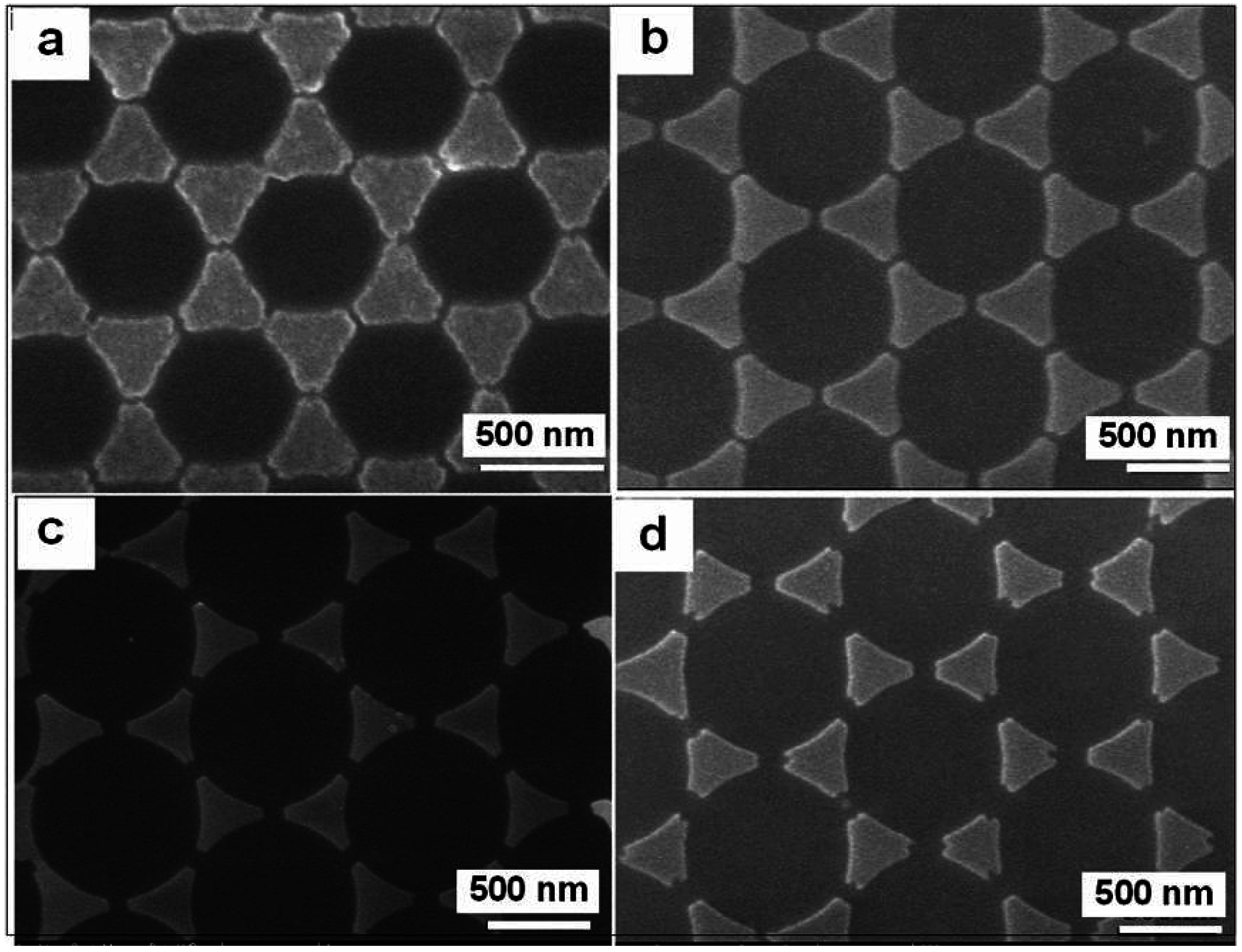
4.3. Au Binary-Structure Arrays from the Colloidal Template with Dualistic Structure

Similarly, if we use the non-close-packed PS colloidal monolayers with the dualistic structure shown in Figure 5b as a template, we could fabricate the binary-structure array built of the hexagonally arranged nanoshells and the nanorings based on the non-shadow sputtering deposition [42]. Briefly, a thin gold layer is first coated on the PS colloidal monolayer via the sputtering deposition with non-shadow effect, similar to the fabrication of Au gold opening nanoshell-ordered arrays (Figure 8). After deposition, in addition to the formation of the nanoshells on the etched PS spheres, the nanorings were also formed surrounding the linking-bars between the adjacent etched PS spheres. Finally, a gold nanoring/nanoshell-built binary structure array was obtained by subsequent removal of the etched PS spheres, via dissolution in CH2Cl2 solution and cleaning. Correspondingly, Figure 10a shows a typical as-prepared array, which consists of hexagonally arranged microspheres, with 820 nm in diameter and 180 nm in spacing, and much smaller plate-like nano-objects nearly vertically standing between the adjacent microspheres. There are six nanoplates in nearly hexagonal distribution surrounding each microsphere. Local magnification has revealed that the nanoplates are circular in shape and about 190 nm in diameter and 40 nm in thickness, and have a hole with about 70 nm in diameter in its centre (the inset of Figure 10a), which are really the nanorings. Further, TEM examination has also confirmed that the microspheres were of the truncated hollow sphere structure, as shown in Figure 10b. Only incomplete spheres were seen, similar to our previous results [29]. Obviously, such binary structured arrays are tunable in their structural parameters, such as shell thickness and curvature, ring’s size, by the deposition conditions and the geometry of PS monolayer.
The formation of the nanoshells in the binary-structured array can be easily understood based on the geometry of the etched PS template and non-shadow deposition. The formation of the nanorings in the array could be attributed to the geometry of the linking-bars or the bridges between two adjacent etched PS spheres. From Figure 5b, we can see that the linking-bars or the bridges are thinner at middle part and thicker at both ends due to the isotropic plasma etching. Therefore, under the condition of non-shadow deposition (usually at a low deposition rate [42]), the deposition would preferentially take place at the thinner part, leading to ring-like or radial growth. Additionally, the surface diffusion of Au atoms that deposited on the linking-bars or bridges could also play a role in formation of the nanorings. Au atoms might deposit on the other parts of the linking-bars or bridges, however, they would migrate to the middle part via surface diffusion due to the difference between the thinner middle part and thicker ends in surface energies. After subsequent removal of PS template by dissolution, the PS linking-bars would disappear and the gold nanorings would lay on the surface of the truncated hollow spheres, as demonstrated in Figure 10a and its inset. Obviously, for the templates without the linking-bars or with too-short bars, no nanoring could be formed.
The optical absorption spectrum was measured for such binary-structured array shown in Figure 10a, as demonstrated in Figure 11a. There exist two absorption peaks on its absorption spectrum, which are around 710 nm and 950 nm, respectively, by fitting according to the Gaussian peak-type. The broad peak around 950 nm should originate from the SPR of the nanoshells, which is in agreement with that reported previously [34]. The peak around 710 nm could be attributed to the SPR mainly from the nearly vertically standing nanoring array.
Further, the discrete dipole approximation (DDA) calculation [43] was carried out to simulate the optical properties of an isolated standing Au nanoring. The structural parameters are as follows: the thickness of nanoring is 40 nm, and the outer and inner diameters are 190 nm and 70 nm, respectively. These parameters are also the average values corresponding to those measured from Figure 10a. The simulated optical absorbance spectrum of the isolated nanoring is shown in Figure 11b, which is in agreement with the measured result (curve (I) in Figure 11a) in the peak shape. The peak from measurement was broader in width and of longer wavelength in position, compared with the simulated one. This could be mainly attributed to the size dispersivity of the nanorings and the coupling effects among them [39].

5. Summary and Remarks

In summary, the self-assembled organic monolayer colloidal crystals could be transferred, in water or solutions, from a glass slide to any other substrate, such as a metal substrate, flexible substrate and so on. We can thus fabricate some nanostructured arrays on these substrates by using the colloidal monolayers as templates. However, the self-assembly-induced colloidal monolayer is arranged in a hexagonal close-packed manner and is hence exclusive in structure, which limits its application in fabrication of the nanostructured arrays. The structural diversity of the polystyrene (PS) colloidal monolayers is thus important for them to be used as the templates for fabrication of various nanostructured arrays. The plasma etching is a flexible and effective way to achieve the structural diversity of such template due to its isotropic etching process. Via plasma bombardment, we can transform the close-packed colloidal crystals into the non-close-packed ones with tunable structural parameters.
Using these modified PS colloidal monolayers as templates or masks, we can fabricate some nanostructured arrays with special and complex structures by material deposition on them, such as the gold triangular nanoplate arrays with controllable spacings, the gold opening-nanoshell arrays with tunable gaps and the nanoshell’s thicknesses, in addition to the gold binary-structure arrays built out of the hexagonally arranged nanoshells and nanorings. These arrays have exhibited the tunable SPR in a large region, subsequently leading to promising potential applications such as in the SPR-based biosensors and surface-enhanced Raman scattering (SERS)-based devices, etc. If more deposition methods and materials are employed, we can produce many more nanostructured arrays with different structures by these modified PS colloidal templates.

Acknowledgments

This work is financially supported by Natural Science Foundation of China (Grant No. 51531006, 11574313, 11374300 and 51571188, and Natural Science Foundation of An Hui Province (Grant No. 1508085MA16), and the CAS/SAF International Partnership Program for Creative Research Teams.

Author Contributions

Guangqiang Liu performed the experiments and wrote the first draft; Weiping Cai conceived and finalized the paper.

Conflicts of Interest

The authors declare no conflict of interest.

References

  1. Reichenbach, P.; Eng, L.M.; Georgi, U.; Voit, B. 3D-steering and superfocusing of second-harmonic radiation through plasmonic nano antenna arrays. J. Laser. Appl. 2012, 24, 042005. [Google Scholar] [CrossRef]
  2. Vontobel, P.O.; Robinett, W.; Kuekes, P.J.; Stewart, D.R.; Straznicky, J.; Williams, R.S. Writing to and reading from a nano-scale crossbar memory based on memristors. Nanotechnology 2009, 20, 425204. [Google Scholar] [CrossRef] [PubMed]
  3. Wang, X.D.; Song, J.H.; Liu, J.; Wang, Z.L. Direct current nanogenerator driven by ultrasonic wave. Science 2007, 316, 102–105. [Google Scholar] [CrossRef] [PubMed]
  4. Hu, Z.J.; Tian, M.W.; Nysten, B.; Jonas, A.M. Regular arrays of highly ordered ferroelectric polymer nanostructures for non-volatile low-voltage memories. Nature Mater. 2009, 8, 62–67. [Google Scholar] [CrossRef] [PubMed]
  5. Li, Y.; Huang, X.J.; Heo, S.H.; Li, C.C.; Choi, Y.K.; Cai, W.P.; Cho, S.O. Superhydrophobic bionic surfaces with hierarchical microsphere/SWCNT composite arrays. Langmuir 2007, 23, 2169–2174. [Google Scholar] [CrossRef] [PubMed]
  6. Masson, J.-F.; Murray-Méthot, M.-P.; Live, L.S. Nanohole arrays in chemical analysis: Manufacturing methods and applications. Analyst 2010, 135, 1483–1489. [Google Scholar] [CrossRef] [PubMed]
  7. Debrina, J.; Abhijit, M.; Goutam, D. High Raman enhancing shape-tunable Ag nanoplates in alumina: A reliable and efficient SERS technique. ACS Appl. Mater. Inter. 2012, 4, 3330–3334. [Google Scholar]
  8. Liu, G.Q.; Cai, W.P.; Kong, L.C.; Duan, G.T.; Li, Y.; Wang, J.J.; Zuo, G.M.; Cheng, Z.X. Standing Ag nanoplate-built hollow microphere arrays controllable structural paramerters and strong SERS performances. J. Mater. Chem. 2012, 22, 3177–3184. [Google Scholar] [CrossRef]
  9. Fu, R.R.; Liu, G.Q.; Jia, C.; Li, X.H.; Tang, X.; Duan, G.T.; Li, Y.; Cai, W.P. Fabrication of silver nanoplate built hierarchical turreted ordered array and the application in trace analyses. Chem. Comm. 2015, 51, 6609–6612. [Google Scholar]
  10. Xu, S.H.; Fei, G.T.; Zhu, X.G.; Wang, B.A.; Wu, B.; Zhang, L.D. A facile and universal way to fabricate superlattice nanowire arrays. Nanotechnology 2011, 22, 265602. [Google Scholar] [CrossRef] [PubMed]
  11. Zhan, Z.B.; Lei, Y. Sub-100-nm nanoparticle arrays with perfect ordering and tunable and uniform dimensions fabricated by combining nanoimprinting with ultrathin alumina membrane technique. ACS Nano 2014, 8, 3862–3868. [Google Scholar] [CrossRef] [PubMed]
  12. Li, Z.W.; Gu, Y.N.; Wang, L.; Ge, H.X.; Wu, W.; Xia, Q.F.; Yuan, C.S.; Chen, Y.; Cui, B.; Williams, R.S. Hybrid nanoimprint−soft lithography with sub-15 nm resolution. Nano Lett. 2009, 9, 2306–2310. [Google Scholar] [CrossRef] [PubMed]
  13. Chen, Y.F. Nanofabrication by electron beam lithography and its applications: A review. Microelectro Eng. 2015, 135, 57–72. [Google Scholar] [CrossRef]
  14. Li, Y.; Duan, G.T.; Liu, G.Q.; Cai, W.P. Physical processes-aided periodic micro/ nanostructured arrays by colloidal template technique: fabrication and application. Chem. Soc. Rev. 2013, 42, 3614–3627. [Google Scholar] [CrossRef] [PubMed]
  15. Wang, J.J.; Duan, G.T.; Li, Y.; Liu, G.Q.; Cai, W.P. Wet etching-assisted colloidal lithography: A general strategy toward nanodisk and nanohole arrays on arbitrary substrates. ACS Appl. Mater. Inter. 2014, 6, 9207–9213. [Google Scholar] [CrossRef] [PubMed]
  16. Liu, G.Q.; Cai, W.P.; Kong, L.C.; Duan, G.T.; Li, Y.; Wang, J.J.; Cheng, Z.X. Trace detection of cyanide based on SERS effect of Ag nanoplate-built hollow microsphere arrays. J. Hazard. Mater. 2013, 248, 435–441. [Google Scholar] [CrossRef] [PubMed]
  17. Li, Y.; Cai, W.P.; Duan, G.T. Ordered micro/nanostructured arrays based on the monolayer colloidal crystals. Chem. Mater. 2008, 20, 615–624. [Google Scholar] [CrossRef]
  18. Ye, X.; Qi, L. Two-dimensionally patterned nanostructures based on monolayer colloidal crystals: Controllable fabrication, assembly, and applications. Nano Today 2011, 6, 608–631. [Google Scholar] [CrossRef]
  19. Vogel, N.; Weiss, C.K.; Landfester, K. From soft to hard: the generation of functional and complex colloidal monolayers for nanolithography. Soft Matter. 2012, 8, 4044–4061. [Google Scholar] [CrossRef]
  20. Vogel, N.; Retsch, M.; Fustin, C.-A.; Campo, A.; Jonas, U. Advances in Colloidal Assembly: The Design of Structure and Hierarchy in Two and Three Dimensions. Chem. Rev. 2015, 115, 6265–6311. [Google Scholar] [CrossRef] [PubMed]
  21. Sun, F.Q.; Cai, W.P.; Li, Y.; Cao, B.Q.; Lei, Y.; Zhang, L.D. Morphology-controlled growth of large-area two-dimensional ordered pore arrays. Adv. Funct. Mater. 2004, 14, 283–288. [Google Scholar] [CrossRef]
  22. Liu, Z.F.; Jin, Z.G.; Liu, W.; Liu, X.X. Ordered porous ZnO thin films formed by dip-coating method using PS templates. J. Sol-Gel. Sci. Tech. 2006, 40, 25–30. [Google Scholar] [CrossRef]
  23. Dai, Z.F.; Li, Y.; Duan, G.T.; Jia, L.C.; Cai, W.P. Phase diagram, design of monolayer binary colloidal crystals, and their fabrication based on ethanol-assisted self-assembly at the air/water interface. ACS Nano 2012, 6, 6706–6716. [Google Scholar] [CrossRef] [PubMed]
  24. Yu, J.; Yan, Q.; Shen, D. Co-self-assembly of binary colloidal crystals at the air-water interface. ACS Appl. Mater. Interface 2010, 2, 1922–1926. [Google Scholar] [CrossRef] [PubMed]
  25. Liu, G.Q.; Cai, W.P.; Kong, L.C.; Duan, G.T.; Lü, F.J. Vertically cross-linking silver nanoplate arrays with controllable density based on seed-assisted electrochemical growth and their structurally enhanced SERS activity. J. Mater. Chem. 2010, 20, 767–772. [Google Scholar] [CrossRef]
  26. Ren, Z.Y.; Li, X.; Zhang, J.H.; Li, W.; Zhang, X.M.; Yang, B. Tunable two-dimensional non-close-packed microwell arrays using colloidal crystals as templates. Langmuir 2007, 23, 8272–8276. [Google Scholar] [CrossRef] [PubMed]
  27. Jiang, P.; McFarland, M.J. Wafer-scale periodic nanohole arrays templated from two-dimensional nonclose-packed colloidal crystals. J. Am. Chem. Soc. 2005, 127, 3710–3711. [Google Scholar] [CrossRef] [PubMed]
  28. Yang, J.L.; Duan, G.T.; Cai, W.P. Controllable fabrication and tunable magnetism of nickel nanostructured ordered porous arrays. J. Phys. Chem. C 2009, 113, 3973–3977. [Google Scholar] [CrossRef]
  29. Liu, G.Q.; Li, X.H.; Wang, W.B.; Zhou, F.; Duan, G.T.; Li, Y.; Xu, Z.K.; Cai, W.P. Gold binary-structured arrays based on monolayer colloidal crystal and their optical properties. Small 2014, 10, 2374–2381. [Google Scholar] [CrossRef] [PubMed]
  30. Sinitskii, A.; Tour, J.M. Patterning graphene through the self-assembled templates: toward periodic two-dimensional graphene nanostructures with semiconductor properties. J. Am. Chem. Soc. 2010, 132, 14730–14732. [Google Scholar] [CrossRef] [PubMed]
  31. Li, Y.; Sasaki, T.; Shimizu, Y.; Koshizaki, N. Hexagonal-close-packed, hierarchical amorphous TiO2 nanocolumn arrays: Transferability, enhanced photocatalytic activity, and superamphiphilicity without UV irradiation. J Am. Chem. Soc. 2008, 130, 14755–14762. [Google Scholar] [CrossRef] [PubMed]
  32. Zhang, X.Y.; Hicks, E.M.; Zhao, J.; Schatz, G.C.; Duyne, R.P.V. Electrochemical tuning of silver nanoparticles fabricated by nanosphere lithography. Nano Lett. 2005, 5, 1503–1507. [Google Scholar] [CrossRef] [PubMed]
  33. Murray, W.A.; Suckling, J.R.; Barnes, W.L. Overlayers on silver nanotriangles: Field confinement and spectral position of localized surface plasmon resonances. Nano Lett. 2006, 6, 1772–1777. [Google Scholar] [CrossRef] [PubMed]
  34. Liu, G.Q.; Li, Y.; Duan, G.T.; Wang, J.J.; Cai, W.P. Tunable surface plasmon resonance and strong SERS performances of Au opening nanoshell ordered arrays. ACS Appl. Mater. Interface 2012, 4, 1–5. [Google Scholar] [CrossRef] [PubMed]
  35. Zimmermann, C.; Feldmann, C.; Wanner, M.; Gerthsen, D. Nanoscale gold hollow spheres through a microemulsion approach. Small 2007, 3, 1347–1349. [Google Scholar] [CrossRef] [PubMed]
  36. Zeng, J.; Huang, J.L.; Lu, W.; Wang, X.P.; Wang, B.; Zhang, S.Y.; Hou, J.G. Necklace-like noble-metal hollow nanoparticle chains: synthesis and tunable optical properties. Adv. Mater. 2007, 19, 2172–2176. [Google Scholar] [CrossRef]
  37. Zhang, J.H.; Yang, B. Patterning colloidal crytals and nanostructure arrays by soft lithography. Adv. Funct. Mater. 2010, 20, 3411–3424. [Google Scholar] [CrossRef]
  38. Konorov, S.O.; Addison, C.J.; Schulze, H.G.; Turner, R.F.B.; Blades, M.W. Hollow-core photonic crystal fiber-optic probes for Raman spectroscopy. Opt. Lett. 2006, 31, 1911–1913. [Google Scholar] [CrossRef] [PubMed]
  39. Kreibig, U.; Vollmer, M. Optical Properties of Metal Clusters; Springer: New York, NY, USA, 1995. [Google Scholar]
  40. Haynes, C.L.; Duyne, R.P.V. Nanosphere lithography: A versatile nanofabrication tool for studies of size-dependent nanoparticle optics. J. Phys. Chem. B 2001, 105, 5599–5611. [Google Scholar] [CrossRef]
  41. Sun, F.Q.; Cai, W.P.; Li, Y.; Duan, G.T.; Nichols, W.T.; Liang, C.H.; Koshizaki, N.; Fang, Q.; Boyd, I.W. Laser morphological manipulation of gold nanoparticle arrays formed by nanosphere lithography. Appl. Phys. B 2005, 81, 765–768. [Google Scholar] [CrossRef]
  42. Duan, G.T.; Lv, F.J.; Cai, W.P.; Luo, Y.Y.; Li, Y.; Liu, G.Q. General synthesis of 2D ordered hollow sphere arrays based on nonshadow deposition dominated colloidal lithography. Langmuir 2010, 26, 6295–6302. [Google Scholar] [CrossRef] [PubMed]
  43. Draine, B.T.; Flatau, P.J. Discrete-dipole approximation for scattering calculation. J. Opt. Soc. Am. A 1994, 11, 1491–1499. [Google Scholar] [CrossRef]
Figure 1. The PS colloidal monolayer with 2 μm in the PS sphere’s diameter on the glass. (a): A photograph of the colloidal monolayer on the glass slide. (b): The scanning electron microscopic (SEM) image corresponding to the area of the rectangular frame marked in (a). The inset is a locally magnified image in the edge region of the slide, showing the monolayer.
Crystals 06 00126 g001
Figure 2. The photos of the PS colloidal monolayer transfer from a glass slide to another substrate. (a): A glass slide covered with PS colloidal monolayer on a slant is slowly put into the distilled water in a cup, and the monolayer is peeling off from the glass and floats on the water’s surface. (b): The colloidal monolayer peels off completely from the glass and floats on the surface of water with good integrity. (c,d): The floating monolayer is being picked up with another substrate (a silicon wafer).
Crystals 06 00126 g002
Figure 3. Morphology of the etched PS colloidal crystals. (a,b): The SEM images of PS monolayer colloidal crystals after Ar+ plasma etching of the as-prepared monolayer, with 350 nm in the original PS sphere’s diameter, for 5 min and 9 min, respectively. The inset in (b): a local cross sectional image. (c): The SEM image of the as-prepared close-packed double-layer PS colloidal crystal with 1 μm in PS sphere’s diameter. (d): The SEM image of (c) after Ar+ plasma etching for 12 min. (input power for the etching was 100 W).
Crystals 06 00126 g003
Figure 4. SEM images of the as-self assembled PS colloidal monolayer after Ar+ plasma etching. (a,b): After etching for 6 min and 7 min., respectively, for the monolayer with 200 nm in initial diameter of PS sphere. (c): After alternately heating (at 120 °C for a few seconds) and etching several times for the monolayer with 120 nm in initial diameter of PS sphere (100 W in input power for etching).
Crystals 06 00126 g004
Figure 5. The morphologies before and after Ar+ plasma etching the heated PS monolayer. (a): The SEM image of the close-packed PS colloidal monolayer with 1 μm in PS sphere diameter on the Si wafer after heating at 120 °C for 2.5 min, showing deformed PS spheres. The inset is a local magnified image. (b): The SEM image after Ar+ plasma etching the PS monolayer in (a) for 10 min (100 W in input power), showing non-close-packed and dualistic structure, and the inset: a magnified image of a single etched PS sphere (Guangqiang Liu et al. [29]).
Crystals 06 00126 g005
Figure 6. The morphology after Ar+ plasma etching the heated PS monolayer for enough time. (a): The SEM image of the heated PS monolayer with 1 μm in PS sphere’s diameter after etching for 12 min. (b): The SEM image of the heated PS monolayer with 2 μm in initial PS sphere’s diameter after etching for 15 min. The insets are the magnified images of the single etched PS spheres. (100 W in input power for etching).
Crystals 06 00126 g006
Figure 7. The SEM images of triangular gold nanoplate arrays with different spacings by sputtering deposition of Au on the hexagonal close-packed PS colloidal monolayers pre-heated at 120 °C for different durations and removing the PS spheres. (a): 0 min. (b): 1 min (c): 2 min. (d): 3 min.
Crystals 06 00126 g007
Figure 8. The morphology and structure of the Au nanoshell array. (a): The SEM image of the as-prepared array, after sputtering deposition of Au on the etched PS monolayer (with 200 nm in the initial PS sphere’s size), for 24 s and removal of PS spheres. (b): The local magnified image of (a). (c): TEM image of the sample shown in (a), and the inset is the corresponding fast Fourier transform. (d): TEM image observed with a slantwise angle for the sample shown in (a) (Guangqiang Liu et al. [34]).
Crystals 06 00126 g008
Figure 9. Optical absorption spectra of the Au opening-nanoshell arrays with different shell thicknesses. Curves (a–f): correspond to the arrays after sputtering deposition for the duration from 20 s to 90 s (or the shell thickness from 2 nm to 9 nm) (Guangqiang Liu et al. [34]).
Crystals 06 00126 g009
Figure 10. The morphology of the as-prepared Au binary-structured array from the colloidal template shown in Figure 5b. (a): The SEM image of the array. The inset is a local magnified image showing one single microsphere with six standing nanorings. (b): TEM image of the nanoshells in (a) (Guangqiang Liu et al. [29]).
Crystals 06 00126 g010
Figure 11. Optical absorbance spectra of the gold binary-structured array shown in Figure 10a. (a): The measured absorbance spectrum. Dash lines (I) and (II) are the results of spectral decomposition by Gaussian peak-type. (b): The absorption spectrum of a standing nanoring simulated by DDA (Guangqiang Liu et al. [29]).
Crystals 06 00126 g011

