Article

The Effect of the Interaction of Intense Low-Energy Radiation with a Zinc-Oxide-Based Material

1
Institute of Physics, Mathematics, Economy and Innovation Technologies, Drohobych Ivan Franko State Pedagogical University, 24 Ivan Franko St., 82100 Drohobych, Ukraine
2
Institute of Materials Engineering, Faculty of Exact and Technical Sciences, University of Rzeszow, Pigonia 1, 35-310 Rzeszow, Poland
3
Institute of Applied Mathematics and Fundamental Sciences, Lviv Polytechnic National University, 12 Stepana Bandery St., 79000 Lviv, Ukraine
*
Author to whom correspondence should be addressed.
Crystals 2025, 15(8), 685; https://doi.org/10.3390/cryst15080685
Submission received: 2 July 2025 / Revised: 25 July 2025 / Accepted: 26 July 2025 / Published: 28 July 2025
(This article belongs to the Section Inorganic Crystalline Materials)

Abstract

Laser annealing of oxide functional thin films makes them compatible with substrates of various types, especially flexible materials. The effects of optical annealing on Ni-doped ZnO thin films were the subject of investigation and analysis in this study. Using pulsed laser deposition, we deposited polycrystalline ZnNiO films on sapphire and silicon substrates. The deposited film was annealed by laser heating. A continuous CO2 laser was used for this purpose. The uniformly distributed long-wavelength radiation of the CO2 laser can penetrate deeper from the surface of the thin film compared to short-wavelength lasers such as UV and IR lasers. After growth, optical post-annealing processes were applied to improve the conductive properties of the films. The crystallinity and surface morphology of the grown films and annealed films were analyzed using SEM, and their electrical parameters were evaluated using van der Pauw effect measurements. We used electrical conductivity measurements and investigated the photovoltaic properties of the ZnNiO film. After CO2 laser annealing, changes in both the crystalline structure and surface appearance of ZnO were evident. Subsequent to laser annealing, the crystallinity of ZnO showed both change and degradation. High-power CO2 laser annealing changed the structure to a mixed grain size. Surface nanostructuring occurred. This was confirmed by SEM morphological studies. After irradiation, the electrical conductivity of the films increased from 0.06 Sm/cm to 0.31 Sm/cm. The lifetime of non-equilibrium charge carriers decreased from 2.0·10−9 s to 1.2·10−9 s.

1. Introduction

The significant demand for efficient and durable optoelectronic devices that operate at short wavelengths has driven substantial attention towards wide-bandgap semiconductors in the past decade. For applications in the ultraviolet range, non-oxide materials such as CdS, ZnSe, ZnS, GaN, etc., have previously been investigated [1]. ZnO is a metal oxide semiconductor with a wide band gap (approximately 3.37 eV at room temperature). It is a very chemically stable material. This makes it a promising material for diverse applications, including optoelectronic devices [2]. Zinc oxide has interesting optical and electrical properties. Features of these materials include high electron mobility, significant exciton binding energy, and low-loss plasmonic characteristics. Transparent conducting oxide (TCO) has been intensively studied for its potential applications in displays [3] and solar cells [4]. Currently, zinc oxide stands out as the most widely used material for TCO applications due to its superior bandwidth and low resistivity.
Thin-film zinc oxide is a key material for the fabrication of ultraviolet photodetectors (UV photodetectors) [5], including photodiodes and photoresistors. UV photodetectors based on transition metal-doped ZnO, in particular nickel-doped ZnO:Ni films [6], have been reported to exhibit improved photoresponse times compared to pure ZnO.
ZnO is predominantly deposited as a thin film with a columnar polycrystalline texture that determines the orientation of the crystallites. Various technologies are used to grow films, including sputtering [7], thermal evaporation [8], electron beam evaporation [9,10], pulsed laser deposition [11], chemical vapor deposition [12], and molecular beam epitaxy [13]. Sputtering technological methods have some advantages: a fairly high deposition rate, stoichiometry and orientation of films on various substrates (including flexible ones), surface smoothness, uniformity, and thickness control.
In general, metal oxide materials (in this case, zinc oxide) are oxygen deficient; and they behave similarly to n-type semiconductors. Oxygen is usually located in face-centered cubic sites in the crystal structure of the material. Therefore, metal oxides lose their structural and electrical properties when oxygen is deficient. The lack of periodic structural properties can cause strain in the crystal lattice, which may be distributed throughout the metal oxide structure. This process causes rapid degradation of optical and conductive properties, which is also attributed to the asymmetric structure caused by oxygen deficiency. To reduce the effects of these effects, ZnO materials are often subjected to technological treatments: for example, thermal annealing or irradiation with high-energy or low-energy rays. These technologies improve the optical and electrical properties after applying rapid thermal and laser annealing processes [14]. Usually, the films after growth require special surface treatments. This treatment increases the stability of the films and reduces the impact of unwanted surface effects. Technological methods of thermal annealing of surfaces require heating samples to high temperatures. Thermal annealing, which is carried out for a sufficiently long time, causes thermal diffusion of defects. However, heating the entire sample has undesirable consequences for device fabrication. Energy radiation from low-energy beams to heavy-ion beams offers a number of advantages in configuring the functional properties of devices. Changing surface properties is required to improve and optimize material behavior for practical applications. Laser surface modification of materials is key to creating new materials. Laser light interacts with the material in a unique way, resulting in permanent changes that are difficult to achieve with other methods. Such laser irradiation can change the crystalline structure and shape of the material, which, in turn, affects its behavior in a particular application. Laser irradiation is a very promising method for low-temperature processing of films. It has several advantages over traditional thermal processes [15,16]. In particular, this applies, for example, to various metal oxides. Laser heating occurs locally and very quickly and can be applied to oxides of various metals, such as TiO2, ZrO2, and SiOx [17,18,19,20,21].
In recent years, laser irradiation has become a key complement to traditional thermal processing. It allows for the rapid initiation of the growth of functional metal oxide (MO) thin films at moderate temperatures. The mechanism involves the absorption of laser radiation, which leads to instantaneous photothermal reactions in the material. This affects the recrystallization and growth kinetics of thin films. Studies have illustrated the development of polycrystalline, textured, and epitaxial microstructures in a range of metal oxide films. The growth of materials like indium tin oxide (ITO), Ga2O3, ZnO, TiO2, VO2, and WO3 has been achieved through techniques such as pulsed laser deposition (PLD), chemical solvent deposition (CSD), and conventional laser sputtering [22,23]. When laser processing involves significant temperature gradients, it leads to a notably high diffusion rate. Consequently, the epitaxial growth rate is orders of magnitude greater, and the effective heating time is considerably reduced. This characteristic distinguishes this process from traditional thermal processing methods. Excimer lasers are frequently employed in studies of ZnO thin film laser annealing due to ZnO’s strong absorption of ultraviolet light. The absorption coefficient of ZnO for a KrF excimer laser (λ = 248 nm) is about 1.2·105 cm−1; thus, the absorption length is about 80 nm. Excimer laser annealing of ZnO films is effective for film thicknesses less than 100 nm. However, excimer laser annealing does not seem to be effective for films of several hundred nanometers. However, with an absorption coefficient of around 120 cm−1 for a CO2 laser, ZnO has an absorption length of approximately 80 μm. Therefore, a CO2 laser (λ = 10.6 μm) is effective for targeting deeper regions of ZnO film. Pulsed excimer lasers offer the advantages of efficient absorption on the surface and less damage to the substrate. Continuous CO2 lasers have the advantage of annealing at a greater depth, but damage to the films has been observed [24]. In general, CO2 lasers have been successfully used for oxide modification and structure growth. In this work, a CO2 laser is used because its coherent light source has a high energy density and can penetrate deep enough into a thin film at a wavelength of 10.6 μm.
Following irradiation, the thin film undergoes several changes, primarily affecting its structural properties. The kinetics of evolution during laser irradiation result from rapid changes in the thermal field. These cause, for example, ultrafast melting, solidification, and redistribution of dopant impurities. In this situation, both the material and spatial appearance of the irradiated structure strongly affect the results of the process. This work aimed to explore the optoelectronic properties of the n-ZnO surface as influenced by energetic photon beam irradiation. The aim of the work is to clarify the mechanisms of the process of low-energy radiation, namely laser irradiation with a CO2 laser beam, on the properties and characteristics of grown ZnNiO thin films. We also address the influence of laser radiation on the structure, as well as the electrical and photovoltaic behavior of ZnNiO thin films.

2. Materials and Methods

Experimental ZnNiO (Ni-doped 5%) films were grown by laser sputtering using a 20 mm diameter ZnNiO target at room temperature. In a sequential process, silicon, quartz, and sapphire substrates were washed using ethanol followed by distilled water. Lateral uniformity and consistent film thickness were achieved by mounting all substrates at an equal radius on a fixture that was rotated about its center. The distance between the target and the substrate was 3 cm.
Laser irradiation was performed using a continuous multimode CO2 laser source (λ = 10.6 μm). The following laser parameters were adopted in the experiment: a power density of 35 W/cm2 (laser beam power of 10 W, beam diameter of 6 mm) and a scanning area of 2.2 mm2. Scanning the samples with the laser beam at 1 mm/s yielded exposure times of 1 s and 5 s for different regions. Thin ZnNiO films are usually transparent in the wavelength range of 0.3–10.6 μm. The energy from the CO2 laser source was not completely absorbed by the samples. The total energy absorbed by the samples was estimated to be about 1 ÷ 5 mJ, respectively. With increasing duration, the energy released into the films increases. An electron microscope in SEM mode was used. Electron microscopy was employed to investigate and characterize the crystal structure of the films. Room temperature was the condition under which most measurements were performed.

3. Results and Discussions

3.1. Laser Annealing Technology

Technological features make laser optical annealing an extremely valuable tool in the production of many electronic components, especially thin films for solar cells, transistors, and other semiconductor devices. In addition, UV-IR optical annealing heat treatment can significantly improve the stress relief and electrical conductivity of ZnO-based samples. A key benefit of these optical annealing processes is their shorter annealing times in comparison to other techniques. Specifically, the 10.6 μm laser annealing technique is noteworthy for its superior deep penetration depth and energy control capabilities. When films are deposited on substrates, there may be a difference in the lattice characteristics of the substrates and thin films. Lattice mismatch, the difference in the dimensions of the crystal structures of the substrate and the thin film, causes unwanted strain or deformation during the thin film fabrication process. The presence of stress or deformation in the thin film can degrade its optical and electrical conductivity properties. The annealing process allows for improved performance of thin films after deposition, effectively reducing the stress at the film–substrate interface.
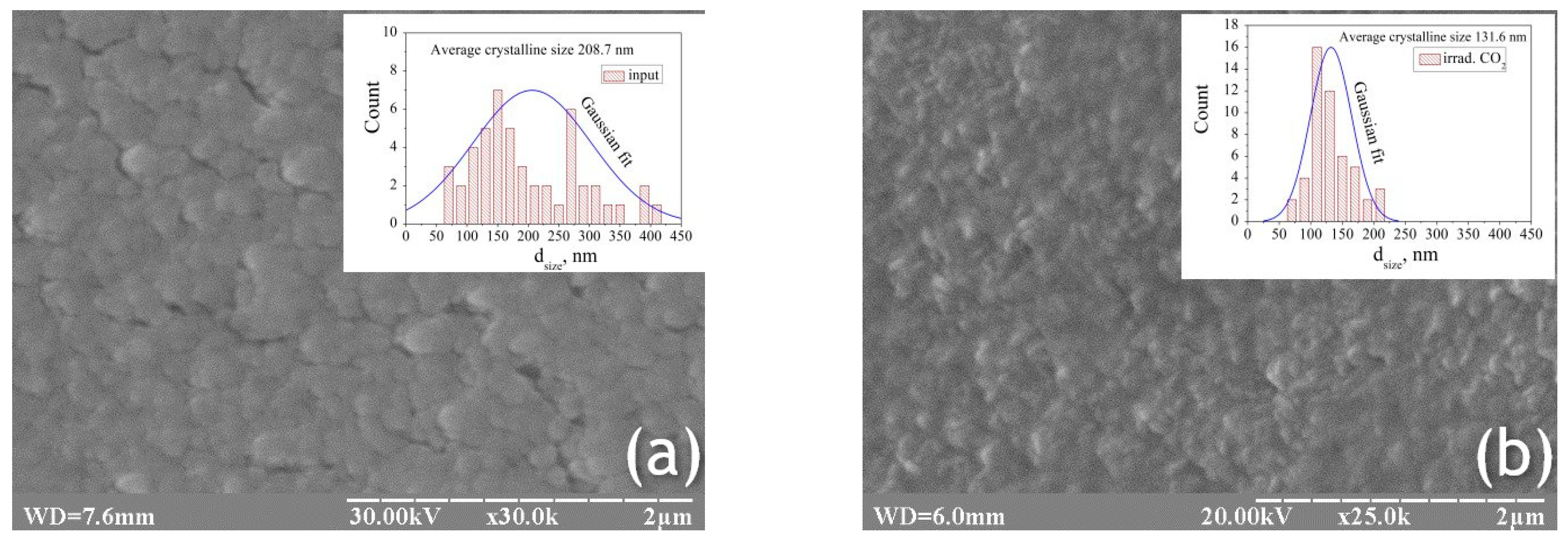
Figure 1a shows the results of microscopy of grown and laser-irradiated ZnNiO films on silicon substrate.
It is evident that each of the ZnNiO films consists of a single ZnO phase, exhibiting a high degree of orientation with the c-axis perpendicular to the substrate surface. ZnO crystallizes in the space group C6v4 (wurtzite) and has two atoms in the unit cell. The lowest surface energy density in the ZnO crystal has the (002) orientation. The tendency for crystal grains with low surface energy to increase in size drives the development of a growth orientation along the crystallographic direction with the lowest surface energy. The observation indicates that the textured film is established under conditions of effective thermodynamic equilibrium. Sufficient surface mobility for the contacting atoms is provided specifically in the (002) direction. Therefore, the film growth process occurs under certain deposition conditions. The images for laser annealing with a wavelength of λ = 10.64 μm in the intensity range I = 10–50 W/cm2 were analyzed. There is a limit on the intensity of Zn nanocrystal formation (Ib = 50 W/cm2) and destruction of the ZnOx film (I > 100 W/cm2). Our findings indicate that laser annealing in the studied range modifies the surface topology. Specifically, as illustrated in Figure 1b, an intensity of 50 W/cm2 during laser annealing results in the formation of nanoislands with a height of around 50 nm and maintains a consistent surface density distribution. The height of the nanoislands was estimated using the standard method of changing sharpness at points along the image depth. However, as a rule, a higher irradiation intensity forms higher nanoislands with lower density.
The preceding information suggests a direct interdependence among mismatch strain, lattice mismatch, and stress. Therefore, the stress was reduced through laser annealing, which decreased the lattice mismatch. Comparing images of different annealing processes, it follows that the crystallites slightly decreased in size after laser annealing. This was attributable to the effects induced by the annealing of the thin film using low-energy laser radiation. Multiple precipitation crystallite deposition of ZnNiO thin films absorbs laser radiation energy, and the crystallite size may also become smaller [25]. As shown in Figure 1b, CO2 laser irradiation results in the features depicted in the diagram, indicating grain growth and a shift in the (002) peak. This peak shift is a consequence of the relaxation of internal stress within the irradiated films [26]. All of the initial films grown in our experiment show some divergence. This demonstrates a correlation between the input energy and both the film deformation on the substrate and the grain size. These changes are also observed in annealed samples [27]. With decreasing irradiation time, both grain sizes and absolute peak intensities increase, and film stresses decrease. Surprisingly, annealing ZnNiO thin films in air can lead to a reduction, instead of an elevation, of the oxygen concentration near the surface. This implies that variations in oxygen content could contribute to the stress reduction seen during annealing. Significant residual stresses are commonly present in deposited thin films. The main source of these stresses is internal stresses, which is determined by the density and structure of the film. It is likely that the high compressive stress inherent in these grown films may be the driving force for grain growth during the laser irradiation process. The compressive stress of the film arises from the high atomic packing density. It can also be a consequence of frozen crystallographic defects in the grains. Given that intragrain defects and grain boundaries have a greater free energy compared to the crystalline structure, grain growth occurs to minimize the system’s free energy.
Laser exposure supplies the thermal energy necessary to reduce the energy in thin layers. During irradiation, the following reactions are possible in them ZnO films: ZnO→ZnZn + VO + 1/2O2, ZnZn→Zni + VZn. Therefore, in irradiated ZnO films, we observed a decrease in stoichiometry, where oxygen vacancies acted as the main donors (VO) and zinc interstitials (Zni). Moreover, the application of sufficient thermal energy induced recrystallization in the ZnO thin films, resulting in enhanced quality. The electrical conductivity properties were also used as an indirect measure of the film’s stoichiometry. Laser irradiation affects the electrical properties of ZnNiO films, demonstrating a reduction in the band gap width. The band gap energy shift can result from the relaxation of mechanical stresses or an increase in defects during laser irradiation, specifically oxygen vacancies or interstitial Zn atoms. It is known that at temperatures close to room temperature, electrical conductivity is mainly the cause of the presence of defects associated with deep-level participation, such as interstitial Zn and oxygen vacancies. The conduction activation energy of ZnO material changes due to crystal defects (dislocations, grain boundaries, point defects). The chemical composition of ZnNiO films obtained by laser sputtering is non-stoichiometric and characterized by an excess of zinc. As a result, these films contain a significant number of lattice defects and surface defects. After irradiation with a CO2 laser, these non-radiative defects can be restructured. Such restructuring makes the crystal structure more perfect and leads to a decrease in the contribution of the conduction mechanism due to defects. Due to laser irradiation, the density of traps in the film is reduced and its crystalline quality is improved. In the case of laser irradiation, a deviation from ideal stoichiometry is observed.

3.2. Electrical Conductivity Properties of Nanostructured ZnNiO Thin Film

To determine the properties of thin films, we measured how their electrical characteristics change with temperature. The four-point probe method was employed to measure the electrical parameters and characteristics. We calculated the electrical conductivity (σ) of the samples from the measured electrical resistance (R). Figure 2 illustrates the variation of ln(σ) with respect to the inverse temperature (1000/T). For comparison, the Arrhenius plot of a laser-irradiated ZnNiO thin film is shown alongside that of an unirradiated film in this figure. As follows from this, the semiconducting nature of all tested films is confirmed by the decrease in their resistance with increasing temperature, in the temperature range of 20–200 °C. The error in measuring electrical resistance was 1%. However, the temperature measurement error, which was 3% in this range, has a greater contribution to the non-monotonicity of the curves.
The room temperature electrical conductivity was measured to be a relatively high 6 × 10⁻² S/cm. This research film is classified as an n-type semiconductor material. This n-type conductivity arises from the presence of inherent defects, specifically interstitial zinc atoms and oxygen vacancies. The increased conductivity in the investigated ZnNiO thin film can be understood by considering that the conductivity of ZnO films originates from electron capture at defects located along the grain boundaries. The observation that the estimated grain size (208 nm) of the synthesized nanostructured ZnNiO is greater than the Debye length (approximately 30 nm for nano ZnO) is indicative of electron accumulation at the grain boundaries. The observed enhancement in electrical conductivity can be attributed to the phenomenon of charge accumulation occurring at the grain boundaries.
The electrical conductivity of the ZnNiO film can be roughly analyzed using the following well-known relationship [28]:
σ ( T ) = σ 0 e E k T
where σ—conductance, σ0—pre-exponential factor, ΔE—activation energy governing electrical conductivity, T—temperature, and k—Boltzmann constant, respectively.
The graphs illustrate a two-stage temperature dependence of the electrical conductivity. To better describe the conductivity mechanism in zinc oxide, the conductivity curve is divided into three different ranges (I, II, and III). Linear region I (low-temperature region) refers to the linear conductivity mechanism, region II is the transition region, and linear region III represents the activation region involved in electrical conductivity. To analyze the electrical conductivity in these areas, the Arrhenius equation can be used, which describes the dependence of electrical conductivity on temperature. The values of E were calculated for regions I and III, respectively, from the linear slopes of the Arrhenius dependence in Figure 2a. The two different conduction mechanisms correspond to two different donor levels at different bandgap positions, which likely explains the observation of the two slopes. Regions I and III correspond to different conduction mechanisms, and in these regions the electrical conductivity increases with increasing temperature. In turn, more and more charge carriers overcome the energy barrier and can be estimated using the Arrhenius equation, which relates electrical conductivity and temperature; this can be represented by the following expression:
σ ( T ) = σ 0 L e E L k T + σ 0 H e E H k T
where σ0L and σ0H—pre-exponential factors and ΔEL and ΔEH—low-temperature and high-temperature activation energies (for low-temperature and high-temperature stages of conductivity, respectively). The activation energies were calculated using the Arrhenius plots, and these values are presented in Table 1 for region I (the low-temperature range of 300–400 K) and region III (the high-temperature range of 400–500 K). The obtained values of ΔEL and ΔEH were 71 meV and 354 meV, respectively. We estimated the activation energy ΔEH to be 354 meV for conduction. This value is much smaller than the optical band gap Eg, which is 3.30 eV. The activation energy values in different temperature regions (e.g., I and III) indicate the presence of two energy levels of donor nature. The values of 71 meV and 354 meV are associated with the energy levels of two shallow donors, respectively, in the band gap of the ZnO semiconductor. Thus, it is estimated that in region III, the electrical conductivity of the ZnNiO thin film is thermally activated by the excitation of electrons from the deeper donor level to the conduction band minimum. The transition region, region II, is characterized by ionization of additional charge carriers from the shallow donor level and ends with their depletion at the transition temperature (Ti). As a result, the electrical conductivity decreases with increasing temperature (Figure 2b), until the activation of charge carriers from the relatively deeper donor level begins [29]. The participation of the jump mechanism through energy barriers created by inhomogeneities (e.g., grain boundaries) at temperatures above room temperature exists, but its contribution is quite small.
In an irradiated ZnNiO thin film, the activation energy (ΔEL and ΔEH) decreases due to changes in electron density from donors. At higher temperatures, electrons gain enough thermal energy to move from the donor levels into the conduction band minimum. Clearly, the thermal activation observed in region I is attributed to deep donor ions. The displacement of O2− ions from their regular lattice sites is expected to result in the creation of oxygen vacancies or zinc interstitials. As donors, these vacancies can also cause lattice deformation to maintain charge neutrality. The measured activation energies for the two regions indicate different mechanisms of trapped or scattered ions. With increasing donor concentration, the activation energy will decrease, which explains the increase in atomic electroactive defects at crystal grain boundaries. Therefore, laser annealing causes a decrease in both the potential barrier height and the activation energy. The reduction in the barrier height at the grain boundaries facilitates charge transfer. However, in the transition region, electrons lack the energy to move from the donor levels to the conduction band. Therefore, conduction occurs due to the movement of electrons in the impurity band, which reduces the contribution of free electrons to the conductivity.
The low-temperature activation energy of ZnNiO samples is likely related to one of the following two donor ionization processes: oxygen vacancy, (VO) VO → V+O + e; or zinc interstitial ionization, Zn + i → Zn+ + i + e. The desorption of O2 particles, which can be described by the reaction O2 → O2 + e, can be a source of activation energy at high temperature. From DC conductivity studies, it is believed that the potential barrier, donor concentration, point defects, and oxygen adsorption–desorption control the conductivity of the ZnO system [30].

3.3. Analysis of Laser Radiation Effects on Crystal Structure, Electrical Properties, and Photoelectric Properties

Laser irradiation had an impact on the electrical properties of ZnNiO films, resulting in increased conductivity. The electrical conductivity of thin films after laser irradiation increases significantly. Table 1 shows the values of the specific electrical conductivity and activation energy for ZnNiO films.
The obtained values are consistent with the ΔE values found in the literature for ZnO [31,32,33]. Laser irradiation causes a decrease in activation energy. The observed decrease in activation energy in the irradiated film can be explained by the increase in the concentration of vacancy-type defects. The increase in the concentration of cations leads to stronger localization of electrons, which directly reduces the activation energy due to the increase in the number of donor centers. In addition, the improved crystallinity of the films may also be a factor in this decrease [34].
The absorption of laser energy occurs mainly due to local accumulations of the metal-containing phase (zinc). The absorbed energy induces defects down to the depth to which the photons reach [35]. The estimation of the radiation absorption Iabs in the grain at parameters α = 120 cm−1 [24] Iabs = I0ꞏ[1 − exp(−αd)] according to Beer’s law gives Iabs = 80 mV/cm2, which is an unacceptably small value compared to the absorption at the grain boundaries. On the other hand, under given irradiation regimes, the diffusion outflow of atoms from the grain boundaries can be estimated by the expression of the diffusion length Ldiff = (DZnꞏtimp)1/2, which is a few nanometers for zinc (DZn = 1.07ꞏ10−14 cm2/s—diffusion coefficient for zinc below melting point [36], timp = 1 s—irradiation pulse duration). That is, it can be stated that all processes occur at existing or potential (defect-enriched) grain boundaries. As a result of local heating, the grain boundaries become more pronounced. Since the heating–cooling cycle of the film is quite short, diffusion of atomic particles, or defects, is possible only on a nanometer scale [37]. The changes caused by the laser are stable when measured again after a few weeks.
The findings from these measurements indicate that the properties of ZnO thin films are contingent upon several parameters, including their stoichiometry and crystallinity. A positive correlation was observed between the intensity of laser irradiation and the electrical conductivity. The trends evident in the experimental conductivity curves can be elucidated by variations in the concentration of electron traps within the film. The energy level and spatial distribution of these traps within the band gap also constitute contributing factors. Specifically, an increase in laser radiation intensity was associated with a decrease in the trap density.

3.4. Photocurrent

Figure 3a,b show the photoelectric current signal waveforms for a thin-film photodetector based on ZnNiO/Al2O
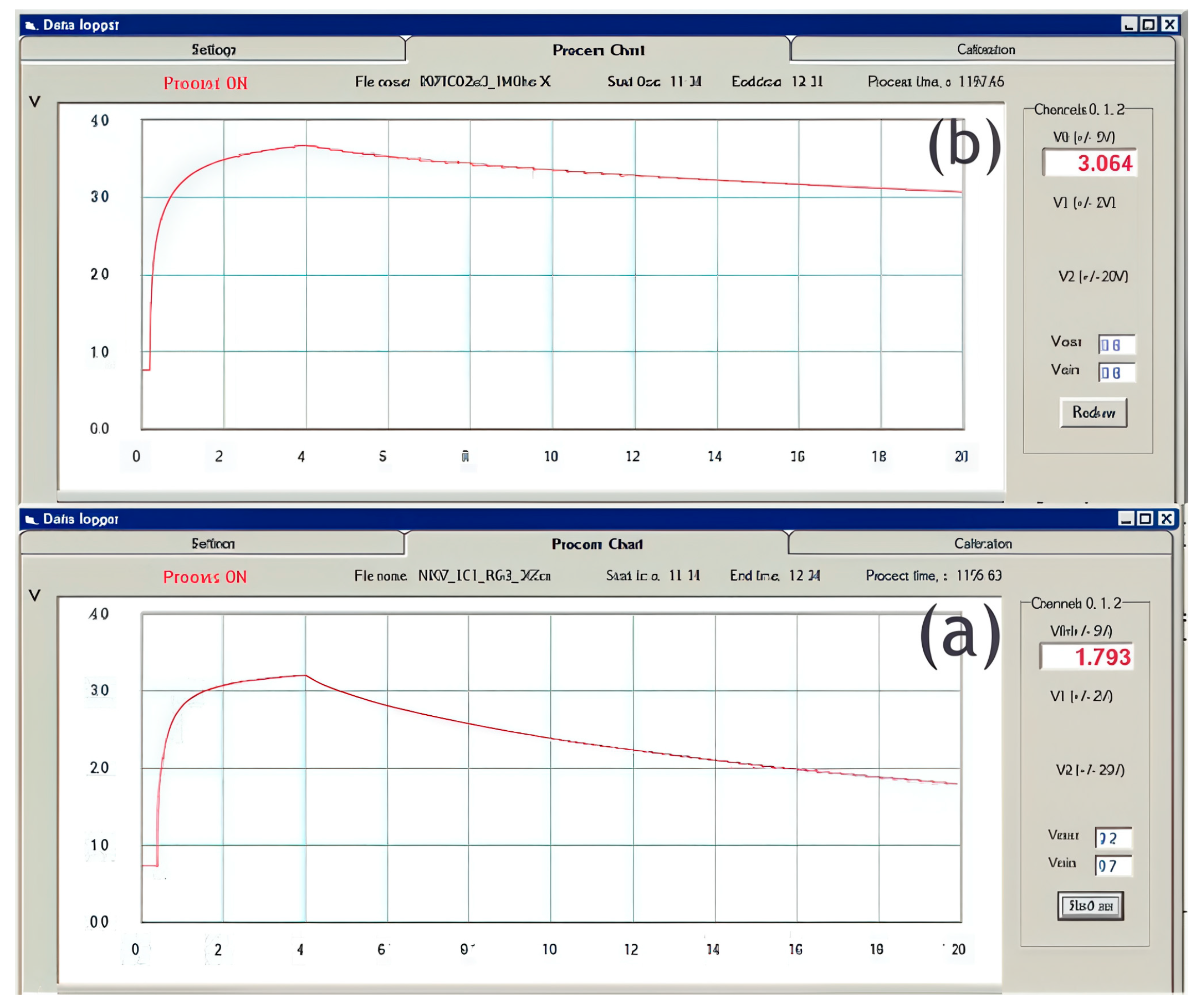
3. The bias voltage is 10 V under ultraviolet illumination with a wavelength of 280 nm.
The dark currents are about 2.5 and 4.1 μA for the original and laser-annealed films, and the photocurrents are about 6.5 and 6.7 μA, respectively. The photocurrent increases rapidly and then gradually saturates (Figure 4a). The decay of the photodetector’s photosignal under a 5 V bias is a rather lengthy process and is influenced by the structural quality of the film. The time-dependent behavior of the photocurrent for the identical thin-film structure is illustrated in Figure 4b using a semi-logarithmic representation. The photocurrent characteristics look asymmetrical. Light exposure causes a gradual loss of oxygen from the ZnO surface, resulting in the development of a surface region characterized by an increasing density of oxygen vacancies (donors). Turning on the light causes the oxygen vacancies to donate electrons. By employing surface doping, electron concentration is accumulated in the surface region. In the absence of light, atmospheric oxygen reacts with the surface, causing the zinc-rich surface to gradually oxidize over time. When ZnO films are irradiated with ultraviolet light, free carriers (electron–hole pairs) are formed. The application of an external electric field causes the movement of these charges towards the electrodes. The polycrystalline structure of the ZnO film promotes the formation of capture centers. They can capture carriers before they are scattered and collected by the electrodes. Initially, there are a large number of capture centers that are slowly filled with carriers generated by ultraviolet light. Consequently, the photocurrent exhibits an increase with longer irradiation times, a phenomenon of carrier capture also referred to as the polarization effect.
The photocurrent exhibits an almost linear increase with increasing applied voltage, since the number of collected charge carriers is linearly proportional to the magnitude of the applied electric field. This observation aligns with a fundamental model explaining the photogeneration and collection of charge carriers [38], and the photocurrent can be mathematically represented as
I p h = q N p h η a b s μ τ E / d
where q—electron charge, Nph—number of incident photons per unit time, ηabs—optical absorption efficiency, μ·τ—product of the mobility of photogenerated charge carriers by the lifetime, d—interelectrode distance, and E—electric field applied to the thin film. The photoconductivity decay analysis indicates that the time constant for the photocurrent to fall to 20% of its maximum is approximately 39 min for the pristine film and extends to around 133 min for the CO2-laser-treated film. Changes in the density of capture centers, which immobilize photogenerated carriers, explain this process. With a lower density of these centers, the probability of carrier recombination decreases, resulting in a prolonged photocurrent decay time. To determine the steady-state sensitivity of the film as a photoresistor, a charge carrier mobility of 80 cm2/V·s was used in the calculation [39]. These calculated values, as well as the estimated lifetime of the charge carriers generated within the film, are provided in Table 2. The approximate value of the μ·τ parameter for the films was calculated to be (1.6 ÷ 1.0)·10−7 cm2/V using Equation (3). ZnNiO films’ photoconductivity parameters are also listed in Table 2.
Therefore, a difference exists in the photocurrent decay behavior between the original and laser-annealed films. This difference can be explained by differences in their structural perfection. Since the grain boundaries are full of traps (defects or impurities) that trap free carriers, the irradiated film has a smaller grain size. After irradiation, the grain boundaries in the original become much larger. Correspondingly, the dark current increases with grain size, while the photocurrent changes only slightly.
Analyzing the temporal kinetics of the photocurrent provides a deeper understanding of the photoprocess. The rise and fall of the photocurrent for excitation with a 4.4 eV (280 nm) LED extends beyond the absorption band gap. At room temperatures, time-differentiated photocurrent dependences dI(t)/dt were plotted for a series of 20 s pulses of excitation of the LEDs. The photocurrent rise is initially relatively fast, passes through a maximum, and then, over a very long time, exhibits a slight decrease. The differentiated temporal kinetics (rise and decay) of the photocurrent under LED excitation are illustrated in Figure 5a. For the decay of the collective of generated charge carriers, which follows exponential dependences of the form I = I0ꞏexp(–t/τ), this representation creates peaks at t = τ. The number of peaks in these graphs corresponds to different relaxation times. By analyzing these curves, it is possible to determine the number of characteristic processes and their corresponding values of τ (time constants).
A positive average dI/dt value upon the onset of illumination confirms the photoconductive behavior of the heterostructure, signifying that the photocurrent increases with time when exposed to UV light. Conversely, the negative average dI/dt value assumes a decrease in photocurrent when the light source is turned off. This observation implies incomplete recombination of charge carriers, which subsequently contributes to the level of dark current associated with the photoconductive phenomenon. The observed differences in dI/dt values between the ON and OFF states reveal the photocurrent response’s sensitivity to light switching. Conversely, the low average dI/dt values for the ZnO structures indicate a slower photocurrent response and less efficient charge carrier movement. These results emphasize the significance of dI/dt behavior in understanding the dynamic photovoltaic characteristics and photoresponse of thin film structures.
The photoconductivity relaxation curves exhibit a stretched exponential behavior, indicating fluctuations in the potential barrier due to carrier trapping:
I p h = I 0 · e x p t τ γ
In Equation (4), I0—value of saturation current, the value does not change over time; the elongation coefficient γ is within 0 < γ ≤ 1. Equation (4) describes how the relaxation time τ changes as the decay progresses over time t. The time dependence of the life expectancy parameter can be expressed by the following equation: τ ( t ) = τ 0 · t 1 γ 0-constant). Specifically, this parameter reflects the broadening of the curve, and its value is governed by the magnitude of the potential barrier fluctuations involved in carrier capture [40]. In this particular case, we plotted the derivative of the photocurrent with respect to the logarithm of time: dI(t)/dln(t). Differentiation with respect to the parameter ln(t) yields peaks at t = τ (Figure 5b), but these peaks exhibit asymmetry and some broadening. This deviates from the case of ideal exponential decay. The extension parameter γ can be quantitatively estimated by fitting the first derivative to the experimentally observed peak profile [41,42].
The relaxation process’s defining features are presented in Figure 5a,b. When the photocurrent increases under 280 nm illumination, the excitation consists of three main processes: a rapid initial increase with a characteristic relaxation time of 0.13 s; a slower increase preceded by the passage of the photocurrent through a maximum value (relaxation time: 13 s); and, with further illumination, a prolonged decrease in the photocurrent (relaxation time: 207 s). The peaks are broad, broader than expected for simple exponential growth processes. The photocurrent initially decayed rapidly, exhibiting a characteristic decay time of 19 s, which is similar to its rapid rise time. Slow peaks can be approximately represented by stretched exponentials rather than simple exponentials, and the expansion factor was a = 0.5. Subsequent to the rapid initial decay, the photocurrent displays a prolonged tail, which is characterized by a time constant of roughly 128 s and is well-described by a stretched exponential function.
The detector structure exhibits a relatively high external quantum efficiency (EQE >> 1). This phenomenon is explained by the strong capture of one type of carrier. Such carriers are identified as holes in our system. This process increases the lifetime of the other type of charge carrier (electrons). These electrons circulate in the circuit and cause an increase in photocurrent. This represents a process that releases trapped charge carriers, making them available for recombination events. Under these conditions, the photocurrent is enhanced. Therefore, the experimental relaxation curves are stretched exponentials, not simple exponentials. This transport mechanism involves the operation of centers with a barrier to electron capture and/or a substantial potential for their fluctuations. Building a detailed model of recombination in semi-insulating photoconductive detectors requires additional research. The remarkably high photosensitivity and EQE exhibited by such photodetectors are attributable to the contribution of trapped photogenerated charge carriers, a phenomenon that inherently results in prolonged relaxation. Growth under Zn-enriched conditions suppresses the formation of VZn. A potential outcome of this is a decrease in trap concentration, which would subsequently diminish the hole trapping effect. However, this can in turn make it challenging to achieve high resistivity and low leakage current due to the increased contribution of zinc interstitials acting as donors.
The use of polycrystalline ZnO films with a high concentration of defects, particularly grain boundary traps, leads to a transient UV response in the photoconductor, characterized by long rise and fall times of the photocurrent. The increase in the fraction of the photocurrent due to the non-radiative decay mechanism can serve as additional direct evidence of this. In dark conditions, atmospheric O2 can adsorb on the ZnOx surface and extract free electrons with the formation of O2. To increase the photoresponse rate, a high-quality ZnO film with a large grain size should be used.

4. Conclusions

The results of this study show that laser irradiation causes changes in the film’s structural morphology, leading to nanostructuring. This arises from the higher density of oxygen vacancies and zinc interstitials in the films. As temperature increases, the electrical conductivity decreases nonlinearly. The temperature-dependent electrical conductivity confirms the semiconductor nature of these samples. The observed temperature dependence of the electrical conductivity in irradiated ZnNiO films indicates a decrease in the band gap. This energy shift can be attributed to residual stress directed along the crystallographic c-axis. The oxygen deficiency effect induced by laser radiation might be responsible for this.
The CO2 laser annealing process can improve the electrical properties (stress relaxation, driven by the diminishing lattice mismatch, leads to this effect). Due to the application of CO2 optical laser annealing, the defects were ionized, which promoted the electrical conductivity process. The laser-annealed ZnNiO thin films improved the electrical conductivity properties by increasing the number of free electrons in the ZnO structure. The photoconductivity growth and decay curves present multiple exponential profiles with lifetimes of 0.23 s, 13 s, and 23 s, respectively, and the lifetime increases to 52 s after pulsed laser annealing. The photoconductivity decay increases from 2.1·103 s to 6.9·103 s. Reducing the film’s lattice mismatch via laser annealing can lead to better electrical and photovoltaic performance. The general changes in the structural, electrical, and photoelectric properties of thin films after laser exposure are presented in Table 3.
The results of our investigations demonstrate that a reduction in the grain size of ZnO films does not inherently guarantee enhanced sensor performance; instead, the crystalline uniformity of the ZnO films is a significant factor in achieving optimal sensor performance. A film with a finer grain usually has a larger surface-area-to-volume ratio, so a higher sensor response is expected. However, the study determined that films with larger grains had better sensor performance, which is intuitively understandable. This deterioration in crystallinity negatively affects the laser-induced grain modification.

Author Contributions

Conceptualization, I.V. and P.P.; methodology, I.V. and P.P.; formal analysis, M.C. and N.B.; investigation, M.C. and N.B.; resources, M.C. and N.B.; data curation, I.V. and P.P.; writing—original draft preparation, I.V., P.P., M.C. and N.B.; writing—review and editing, P.P.; supervision, I.V.; project administration, I.V. and P.P. All authors have read and agreed to the published version of the manuscript.

Funding

This research received no external funding.

Data Availability Statement

The original contributions presented in this study are included in the article. Further inquiries can be directed to the corresponding author.

Conflicts of Interest

The authors declare no conflicts of interest.

Abbreviations

The following abbreviations are used in this manuscript:
TCOTransparent conducting oxide
MOMetal oxide
PLDPulse laser deposition
EQEExternal quantum efficiency

References

  1. Zahoor, R.; Jalil, A.; Ilyas, S.Z.; Ahmed, S.; Hassan, A. Optoelectronic and solar cell applications of ZnO nanostructures. Results Surf. Interfaces 2021, 2, 100003. [Google Scholar] [CrossRef]
  2. Özgür, Ü.; Hofstetter, D.; Morkoç, H. ZnO Devices and Applications: A Review of Current Status and Future Prospects. Proc. IEEE 2010, 98, 1255–1268. [Google Scholar] [CrossRef]
  3. Nguyen, V.C.; Kim, J.; Dang, P.T.; Zumuukhorol, M.; Cuong, T.V.; Hong, C.-H.; Lee, J.-H. Application of a ZnO nanorod layer to display retarder: Dependence of the optical property on synthesis conditions. Opt. Mater. Express 2020, 12, 3315–3327. [Google Scholar] [CrossRef]
  4. Dash, R.; Mahender, C.; Sahoo, P.K.; Soam, A. Preparation of ZnO layer for solar cell application. Mater. Today Proc. 2021, 41, 161–164. [Google Scholar] [CrossRef]
  5. Li, G.; Cheng, B.; Zhang, H.; Zhu, X.; Yang, D. Progress in UV Photodetectors Based on ZnO Nanomaterials: A Review of the Detection Mechanisms and Their Improvement. Nanomaterials 2025, 15, 644. [Google Scholar] [CrossRef]
  6. Abbasi, F.; Zahedi, F.; Yousefi, M.H. Fabricating and investigating high photoresponse UV photodetector based on Ni-doped ZnO nanostructures. Opt. Commun. 2021, 482, 126565. [Google Scholar] [CrossRef]
  7. Mazwan, M.; Ng, S.S.; Samsol Baharin, M.S.N.; Pakhuruddin, M.Z.; Abu Bakar, A.S.; Rahman, M.N.A.; Al- Zuhairi, O.; Abd Rahim, A.F. Radio frequency magnetron sputtering growth of Ni-doped ZnO thin films with nanocolumnar structures. J. Cryst. Growth 2024, 644, 127835. [Google Scholar] [CrossRef]
  8. Hong, R.; Xu, L.; Wen, H.; Chen, J.; Liao, J.; You, W. Control and characterization of structural and optical properties of ZnO thin films fabricated by thermal oxidation Zn metallic films. Opt. Mater. 2012, 34, 786–789. [Google Scholar] [CrossRef]
  9. Yang, S.-D.; Zheng, Y.-X.; Yang, L.; Liu, Z.-H.; Zhou, W.-J.; Wang, S.-Y.; Zhang, R.-J.; Chen, L.-Y. Structural and optical properties of highly (110)-oriented non-polar ZnO evaporated films on Si substrates. Appl. Surf. Sci. 2017, 421, 891–898. [Google Scholar] [CrossRef]
  10. Varnamkhasti, M.G.; Fallah, H.R.; Zadsar, M. Effect of heat treatment on characteristics of nanocrystalline ZnO films by electron beam evaporation. Vacuum 2012, 86, 871–875. [Google Scholar] [CrossRef]
  11. Khudiar, A.I.; Ofuia, A.M. Effect of pulsed laser deposition on the physical properties of ZnO nanocrystalline gas sensors. Opt. Mater. 2021, 115, 111010. [Google Scholar] [CrossRef]
  12. Phan, T.-L.; Cuong, L.V.; Lam, V.D.; Dang, N.T. Various CVD-grown ZnO nanostructures for nanodevices and interdisciplinary applications. Beilstein J. Nanotechnol. 2024, 15, 1390–1399. [Google Scholar] [CrossRef]
  13. Kennedy, O.W.; Coke, M.L.; White, E.R.; Shaffer, M.S.P.; Warburton, P.A. MBE growth and morphology control of ZnO nanobelts with polar axis perpendicular to growth direction. Mater. Lett. 2018, 212, 51–53. [Google Scholar] [CrossRef]
  14. Kang, J.; Koh, J.-H. The effect of Ga doping on ZnO thin films subjected to CO2 laser annealing. Ceram. Int. 2020, 46, 10603–10609. [Google Scholar] [CrossRef]
  15. Hong, R.; Wei, C.; He, H.; Fan, Z.; Shao, J. Influences of CO2 laser irradiation on the structure and photoluminescence of zinc oxide thin films. Thin Solid Film. 2005, 485, 262–266. [Google Scholar] [CrossRef]
  16. Awatif, S.J.; Sahar, N.R.; Ayad, J.A. Study the Interaction of CO2 Laser with ZnO Thin Films and Its Effect on Its Topographic and Optical Properties. In Proceedings of the First International and the Third Scientific Conference 2018, Bali, Indonesia, 18–19 October 2018; Volume 17–18/XI, pp. 139–146. [Google Scholar]
  17. Gavrylyuk, O.O.; Semchuk, O.Y.; Steblova, O.V.; Evtukh, A.A.; Fedorenko, L.L.; Bratus, O.L.; Zlobin, S.O.; Karlsteen, M. Influence of laser annealing on SiOx films properties. Appl. Surf. Sci. 2015, 336, 217–221. [Google Scholar] [CrossRef]
  18. Wesang, K.; von Witzendorff, P.; Hohnholz, A.; Suttmann, O.; Kaierle, S.; Overmeyer, L. Functional coatings of sol-gel on glass substrate using CO2 laser irradiation. Procedia CIRP 2018, 74, 386–389. [Google Scholar] [CrossRef]
  19. Hou, Y.; Jayatissa, A.H. Effect of laser irradiation on gas sensing properties of sol–gel derived nanocrystalline Al-doped ZnO thin films. Thin Solid Films 2014, 562, 585–591. [Google Scholar] [CrossRef]
  20. Desens, M.; Wesang, K.; Hohnholz, A.; Jäschke, P.; Kaierle, S.; Overmeyer, L. Homogeneous annealing of TiO2, ZrO2 and ITO sol-gel layers with CO2 laser. Procedia CIRP 2020, 94, 905–909. [Google Scholar] [CrossRef]
  21. Wesang, K.; Hohnholz, A.; Jahn, R.; Steenhusen, S.; Löbmann, P. Systematic Comparison of Thermal Annealing and Laser Treatment of TiO2 Thin Films Prepared by Sol-Gel Processing. Lasers Manuf. Mater. Process. 2019, 6, 387–397. [Google Scholar] [CrossRef]
  22. Liu, S.; Liu, C.R. Morphology Control by Pulsed Laser in Chemical Deposition Illustrated in ZnO Crystal Growth. Cryst. Growth Des. 2019, 19, 2912–2918. [Google Scholar] [CrossRef]
  23. Patel, S.S.; Mistry, B.V.; Zinzuvadiya, S.; Joshi, U.S. Photon irradiation effects on electrical properties of n-ZnO/p-Si junctions for optoelectronic device. Indian J. Pure Appl. Phys. 2020, 58, 667–672. [Google Scholar]
  24. Yamasaki, K.; Ikenoue, H.; Shimogaki, T.; Watanabe, Y.; Nakamura, D.; Okada, T. High quality ZnO film formation by CO2 laser annealing of buried films in SiO2 matrix. Proc. of SPIE 2014, 8967, 303–308. [Google Scholar]
  25. Yun, J.; Bae, M.-S.; Baek, J.S.; Kim, T.W.; Kim, S.-J.; Koh, J.-H. Modeling of Optimized Lattice Mismatch by Carbon-Dioxide Laser Annealing on (In, Ga) Co-Doped ZnO Multi-Deposition Thin Films Introducing Designed Bottom Layers. Nanomaterials 2023, 13, 45. [Google Scholar] [CrossRef] [PubMed]
  26. Agrohiya, S.; Singh, R.; Dahiya, S.; Rawal, I.; Ohlan, A.; Punia, R.; Maan, A.S. Self-powered solar-blind UV photodetectors based on Zn:NiO/p-Si heterojunction devices. Appl. Phys. A 2023, 129, 233. [Google Scholar] [CrossRef]
  27. Arab, L.; Amri, A.; Meftah, A.; Latif, A.; Tibermacine, T.; Sengouga, N. Effect of the annealing process on the properties of ZnO thin films prepared by the sol-gel method. Chem. Phys. Impact 2023, 7, 100266. [Google Scholar] [CrossRef]
  28. Benhaliliba, M.; Benouis, C.E.; Aida, M.S.; Yakuphanoglu, F.; Sanchez Juarez, A. Indium and aluminium-doped ZnO thin films deposited onto FTO substrates: Nanostructure, optical, photoluminescence and electrical properties. J. Sol-Gel Sci. Technol. 2010, 55, 335–342. [Google Scholar] [CrossRef]
  29. Caglar, M.; Ilican, S.; Caglar, Y.; Yakuphanoglu, F. Electrical conductivity and optical properties of ZnO nanostructured thin film. Appl. Surf. Sci. 2009, 255, 4491–4496. [Google Scholar] [CrossRef]
  30. Godavarti, U.; Mote, V.D.; Dasari, M. Role of cobalt doping on the electrical conductivity of ZnO nanoparticles. J. Asian Ceram. Soc. 2017, 5, 391–396. [Google Scholar] [CrossRef]
  31. Oba, F.; Choi, M.; Togo, A.; Tanaka, I. Point defects in ZnO: An approach from first principles. Sci. Technol. Adv. Mater. 2011, 12, 034302. [Google Scholar] [CrossRef]
  32. Schmidt-Mende, L.; MacManus-Driscoll, J.L. ZnO—Nanostructures, defects, and devices. Mater. Today 2007, 10, 40–48. [Google Scholar] [CrossRef]
  33. Rathnasekara, R.; Mayberry, G.M.; Hari, P. Deep-Level Transient Spectroscopy Studies on Four Different Zinc Oxide Morphologies. Crystals 2024, 14, 224. [Google Scholar] [CrossRef]
  34. Vempati, S.; Mitra, J.; Dawson, P. One-step synthesis of ZnO nanosheets: A blue-white fluorophore. Nanoscale Res. Lett. 2012, 7, 470. [Google Scholar] [CrossRef] [PubMed]
  35. Nedyalkov, N.; Koleva, M.; Nikov, R.; Atanasov, P.; Nakajima, Y.; Takami, A.; Shibata, A.; Terakawa, M. Laser nanostructuring of ZnO thin films. Appl. Surf. Sci. 2016, 374, 172–176. [Google Scholar] [CrossRef]
  36. Parmar, N.S.; Boatner, L.A.; Lynn, K.G.; Choi, J.-W. Zn Vacancy Formation Energy and Difusion Coefcient of CVT ZnO Crystals in the Sub-Surface Micron Region. Sci. Rep. 2018, 8, 13446. [Google Scholar] [CrossRef] [PubMed]
  37. Jain, S.; Medlin, W.; Uprety, S.; Isaacs-Smith, T.; Olsson, T.; Davis, J.; Burrows, S.; Chumley, S.; Park, M.; Laurent, G.M. Nanosecond-laser annealing of zinc oxide thin-films: The effect of the laser wavelength and fluence. Thin Solid Film. 2024, 791, 140236. [Google Scholar] [CrossRef]
  38. Liu, J.M.; Xia, Y.B.; Wang, L.J.; Su, Q.F.; Shi, W.M. Effect of grain size on the electrical properties of ultraviolet photodetector with ZnO/diamond film structure. J. Cryst. Growth 2007, 300, 353–357. [Google Scholar] [CrossRef]
  39. Jayah, N.A.; Yahaya, H.; Mahmood, M.R.; Terasako, T.; Yasui, K.; Hashim, A.M. High electron mobility and low carrier concentration of hydrothermally grown ZnO thin films on seeded a-plane sapphire at low temperature. Nanoscale Res. Lett. 2015, 10, 7. [Google Scholar] [CrossRef]
  40. Chen, L.; Mao, S.; Wang, P.; Yao, Z.; Du, Z.; Zhu, Z.; Belfiore, L.A.; Tang, J. Visible Light Driven Hot-Electron Injection by Pd Nanoparticles: Fast Response in Metal–Semiconductor Photodetection. Adv. Optical Mater. 2021, 9, 2001505. [Google Scholar] [CrossRef]
  41. Yu, G.H.; Fan, X.W.; Guan, Z.P.; Zhang, J.Y.; Zhao, X.W.; Shen, D.Z.; Zheng, Z.H.; Yang, B.J.; Jiang, D.S.; Chen, Y.B.; et al. Photocurrent derivative spectra of ZnCdSe-ZnSe double multi-quantum wells. J. Electron. Mater. 1999, 28, 563–566. [Google Scholar] [CrossRef]
  42. Pecunia, V.; Zhao, J.; Kim, C.; Tuttle, B.R.; Mei, J.; Li, F.; Peng, Y.; Huq, T.N.; Hoye, R.L.Z.; Kelly, N.D.; et al. Assessing the Impact of Defects on Lead-Free Perovskite-Inspired Photovoltaics via Photoinduced Current Transient Spectroscopy. Adv. Energy Mater. 2021, 11, 2003968. [Google Scholar] [CrossRef]
Figure 1. Surface morphology of laser-annealed ZnNiO films: (a) initial ZnNiO/Si, (b) irradiated with a CO2 laser.
Crystals 15 00685 g001
Figure 2. Temperature dependences of electrical conductivity: of the original (1) and laser-annealed (2) thin film of ZnNiO (a). Corresponding temperature dependences of electrical resistance (b).
Crystals 15 00685 g002
Figure 3. Oscillograms of photocurrent under LED illumination with a wavelength of 280 nm of laser-annealed ZnNiO films: (a) original ZnNiO, (b) irradiated with a CO2 laser.
Crystals 15 00685 g003
Figure 4. Photocurrent kinetics under LED illumination with a wavelength of 280 nm of a ZnNiO thin film (1) and a laser-annealed (2) ZnNiO thin film: (a) in linear coordinates, (b) in semi-logarithmic coordinates.
Crystals 15 00685 g004
Figure 5. Kinetics of the derivative of the photocurrent value under LED illumination with a wavelength of 280 nm of a thin film of ZnNiO (1) and a laser-annealed (2) thin film of ZnNiO: (a) in coordinates dIph/dt ÷ t, (b) in coordinates dIph/dln(t) ÷ ln(t). For illustration, photocurrent signals are shown; a dashed line indicates the right vertical axis.
Crystals 15 00685 g005
Table 1. The specific electrical conductivities and activation energies for ZnNiO thin films on sapphire substrates, analyzed for both unirradiated and CO2-laser-irradiated samples.
Thin Filmσ300K, Sm/cmσ0L, Sm/cmσ0H, Sm/cmTi, K ΔEL,
meV
ΔEH,
meV
input0.06 0.80260036871354
Irradiated by CO2 laser0.311.935739057247
Table 2. Photoconductive properties of ZnNiO thin films (unirradiated and irradiated with a CO2 laser).
Thin Filmμ·τ·10−7, cm2/Vτ·10−9, s
Input1.62.0
Irradiated by CO2 laser1.01.2
Table 3. Summary table of changes in structural, electrical, and photoelectric properties of ZnNiO thin films after exposure to CO2 laser.
Thin FilmAverage Crystalline Size, nmσ300K, Sm/cmΔE300K, meVτ·10−9, s
Input208.70.06712.0
Irradiated by CO2 laser131.60.31571.2
Disclaimer/Publisher’s Note: The statements, opinions and data contained in all publications are solely those of the individual author(s) and contributor(s) and not of MDPI and/or the editor(s). MDPI and/or the editor(s) disclaim responsibility for any injury to people or property resulting from any ideas, methods, instructions or products referred to in the content.

