Article

Fabrication and Ultraviolet Response Characteristics of All-Oxide Bi2O3/Ga2O3 Heterojunction

1
School of Physics and Electronic Information, Guangxi Minzu University, Nanning 530006, China
2
School of Medical Imaging, Wannan Medical College, Wuhu 241002, China
3
College of Elementary Education, Nanning Normal University, Nanning 530299, China
*
Authors to whom correspondence should be addressed.
Crystals 2025, 15(7), 601; https://doi.org/10.3390/cryst15070601 (registering DOI)
Submission received: 1 April 2025 / Revised: 30 May 2025 / Accepted: 23 June 2025 / Published: 27 June 2025

Abstract

Heterojunctions are commonly used in optoelectronic devices to improve device performance. However, interface defects and lattice mismatch often hinder carrier transport and reduce efficiency, emphasizing the need for further exploration of diverse heterojunction structures. In this study, a heterojunction device constructed from Bi2O3 and Ga2O3 is demonstrated. The microstructures and photoelectrical properties of Bi2O3 and Ga2O3 thin films were investigated. Bi2O3 and Ga2O3 thin films show a bandgap of 3.19 and 5.10 eV. The Bi2O3/Ga2O3 heterojunction-based device demonstrates rectification characteristics, with a rectification ratio of 2.72 × 10³ at ±4.5 V and an ON/OFF ratio of 1.07 × 10⁵ (4.5/−3.9 V). Additionally, we fabricated a sandwich-structured photodetector based on the Bi2O3/Ga2O3 heterojunction and investigated its ultraviolet photoresponse performance. The photodetector exhibits low dark current (0.34 pA @ 3.9 V) and fast response rise/fall time (<40/920 ms). This work offers important perspectives on the advancement of large-area, low-cost, and high-speed Bi2O3 film-based heterojunction photodetectors.

1. Introduction

The fundamental mechanisms of heterojunction devices mainly rely on the band structures and carrier transport properties of different semiconductor materials, which contributes to their widespread use in high-speed switching devices, solar cells, photodetectors, and more [1,2,3,4,5,6,7]. For heterojunction photodetectors, due to the differing energy band structures of the two materials, band bending and interfacial charge distribution are formed, leading to the generation of a built-in electric field. When suitable light illuminates the heterojunction photodetectors, photons are absorbed by the semiconductor, generating electron-hole pairs. Under the influence of a built-in electric field, the carriers transport in opposite directions, reach the electrode, and form a photocurrent. The inherent characteristics of heterojunctions enable heterojunction photodetectors to achieve high photoresponse performance, such as fast response, high gain, and even self-powering capabilities. Ultraviolet (UV) photodetectors as one important type of photodetectors have attracted tremendous attention due to the demand for missile tracking, scientific analysis, ozone hole monitoring, flame detecting, and so on [8,9,10,11]. Recently, wide-bandgap semiconductor materials have emerged as a promising choice and present rapidly development in UV detection [5,12]. Among the heterojunction UV photodetectors, type I (stradding) band alignments are usually constructed to improve the carrier separation efficiency [13].
Bi2O3, as a p-type metal oxide semiconductor material, possesses many intriguing properties such as wide bandgap, strong light absorption, non-toxic nature, and environmental stability, thereby exhibiting great potential for UV detection [14,15,16,17]. There are four main polymorphs of Bi2O3, namely α-, β-, γ-, and δ-, corresponding to monoclinic, tetragonal, body-centered cubic, and face-centered cubic, respectively [16,18,19,20]. Two-dimensional γ- Bi2O3 UV photodetector has been reported and has shown promising UV detection ability with a responsivity of 64.5 A/W and an ultrafast response speed of 0.29 ms (rise time)/0.87 ms (fall time) [21]. Praveen et al. reported a β-Bi2O3/0D SnO2 quantum dot heterojunction UV detection device by combining an electrospinning technique and facile-one step hydrothermal process, which exhibits a responsivity of 62.5 μA/W and a detectivity of 4.5 × 10⁹ Jones [22]. However, the reported Bi2O3-based photodetectors are mainly based on nanoscale Bi2O3 material. Bi2O3 film-based photodetectors, especially heterojunction photodetectors, are rare, which is mainly attributed to Bi2O3’s poor conductivity. The conductivity of Bi2O3 films is very sensitive to both the deposition technique and deposition conditions [23]. Regarding the high performance mentioned above, it is necessary to investigate the heterojunction formed between the p-type material Bi2O3 and an n-type material.
Gallium oxide (Ga2O3) is regarded as a promising candidate for electronic applications due to its large bandgap (~4.9 eV), high critical breakdown field, and large Baliga figure of merit, which make it suitable for next-generation high-power electronics [24,25]. Achieving stable p-type doping in Ga2O3 remains a significant challenge due to the existence of shallow donor states [26]. It is reported that the CuMO2/Ga2O3 heterojunction self-powered photodetector demonstrates a high photo/dark current ratio of 2.3 × 10⁴, a responsivity of 25 μA/W, and a detectivity of 0.9 × 10¹¹ Jones [27]. Wang reported that the Ga2O3/ZnO heterojunction exhibits a responsivity and detectivity of 2.69 mA/W and 1.56 × 10¹⁰ Jones, and an ultrafast response time of rise/decay time with 56.6/43.4 ms under the regulation of piezoelectricity [28]. Although Ga2O3-based heterojunction has been reported in quantities, it is a great challenge to commercialization due to the inherent defects of heterostructure, such as lattice mismatch, which would lead to heterojunction interface degradation and result in the failure of heterojunctions [29,30,31]. Moreover, high-performance Ga2O3-based UV photodetectors depend on expensive substrates and equipment, which present significant challenges for large-area fabrication [32]. Therefore, there is a need to explore a wider range of heterojunctions.
The properties of Bi2O3 and Ga2O3—UV absorption property, comparable bandgap, and conductive type—make them excellent candidates for UV detection and to form a p-n heterostructure. Moreover, Ga2O3 and Bi2O3 are likely to form type I band alignments because the electron affinities are 3.2 eV for Ga2O3 and 4.9 eV for Bi2O3 [13,22,33]. Further, the basic characteristics of heterojunctions and UV response characteristics of Bi2O3/Ga2O3 heterojunction remain unclear. Therefore, in this work, thin-film-based transparent heterojunction was realized using p-type Bi2O3 and n-type Ga2O3 preparation on a glass substrate, which exhibits potential to detect UV light. The microstructures and photoelectrical properties of Bi2O3 and Ga2O3 thin films were investigated. The film-based Bi2O3/Ga2O3 heterojunction exhibits a high rectification ratio and UV response behavior. The results were a breakthrough in development of large-area and low-cost Bi2O3 film-based heterojunction UV photodetectors.

2. Experimental Procedure

Bi2O3/Ga2O3 heterojunction was synthesized via the magnetron sputtering technique, and the sputtering parameters are listed in Table 1. First, ITO glass substrates (3 cm × 3 cm) were ultrasonically cleaned with acetone, methanol, and then deionized water, before being dried in compressed N2. After that, the Bi2O3 layer was deposited by radio frequency (RF) magnetron sputtering in an Ar atmosphere with a power of 60 W and a pressure of 0.6 Pa. Then, the Ga2O3 layer was deposited on top of the Bi2O3 layer using the same system. The power and sputtering pressure used in the deposition of Ga2O3 were 150 W, 0.5 Pa, respectively. Finally, the patterned ITO top electrode was deposited on the surface of the Ga2O3 layer by direct current magnetron sputtering, utilizing a stainless steel mask for precise patterning. Before all sputtering, the chamber was pumped down to a base pressure of 4 × 10⁻⁴ Pa. During device fabrication, Bi2O3 and Ga2O3 thin films were simultaneously prepared on glass substrates for microstructural and photoelectrical characterization. In addition, to verify the successful preparation of the Ga2O3 film, the individual Ga2O3 film was annealed at 800 °C in air for 2 h. The Bi2O3/Ga2O3 heterojunction devices were synthesized at room temperature and not annealed.
The as-grown samples were characterized by field emission scanning electron microscopy (SEM; Sigma 300, ZEISS, Oberkochen, Germany), X-ray diffraction analyses (XRD; D8 ADVANCE A25, Bruker, Karlsruhe, Germany), a UV–Vis spectrophotometer (UV-2700, Shimadzu, Kyoto, Japan), and X-ray photoelectron spectroscopy (XPS; Escalab 250xi, Thermo Fisher Scientific, East Grinstead, UK). A photoelectric test system comprising an LED lamp, probe station, and Keithley 2602B was used to evaluated the photoelectric characteristics of the fabricated devices. The optical power of LED-emitted radiation was accurately calibrated with a power meter (PM 100D, Thorlabs GmbH., Newton, NJ, USA). Photoresponse testing of the fabricated photodetectors was conducted at room temperature.

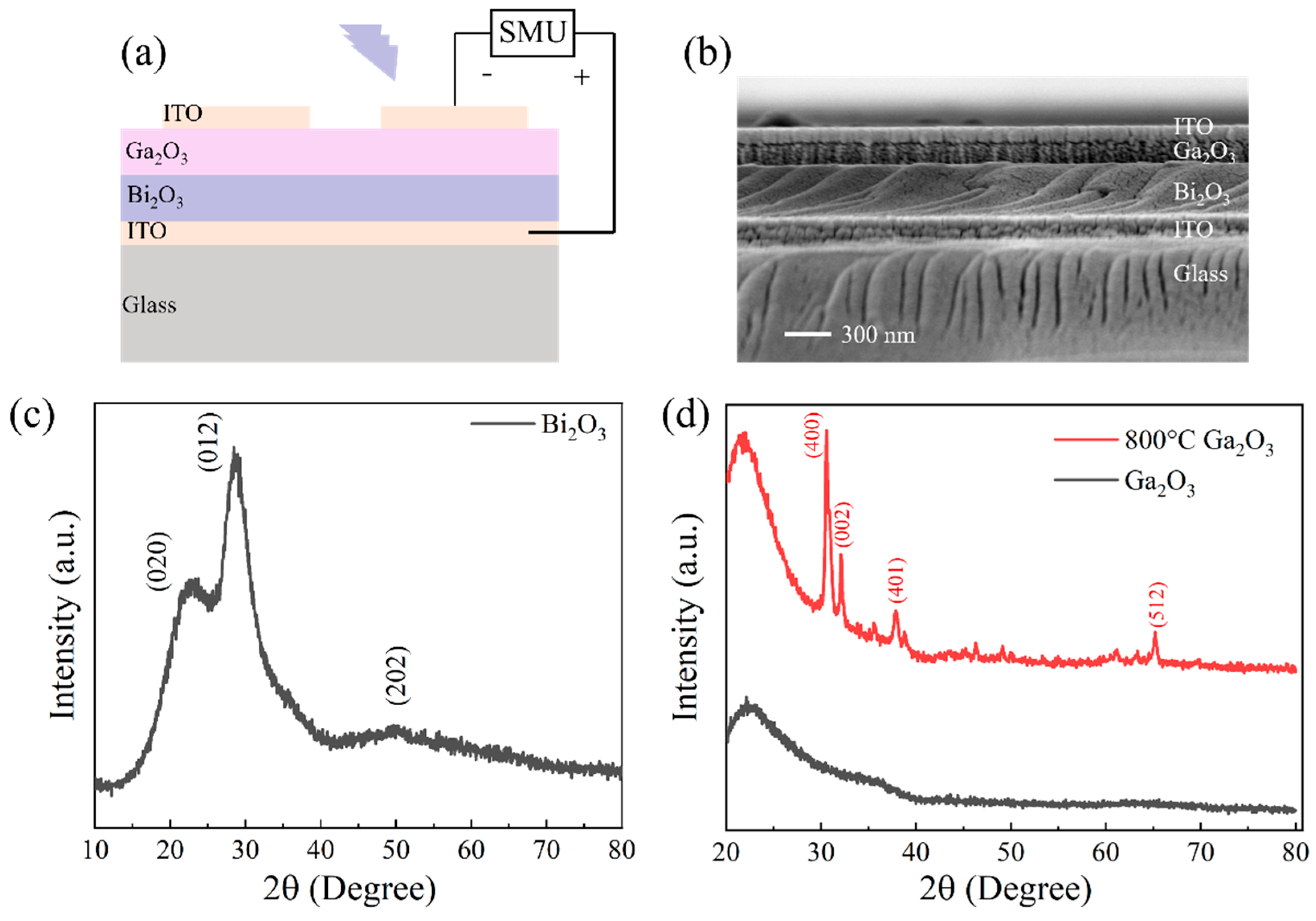
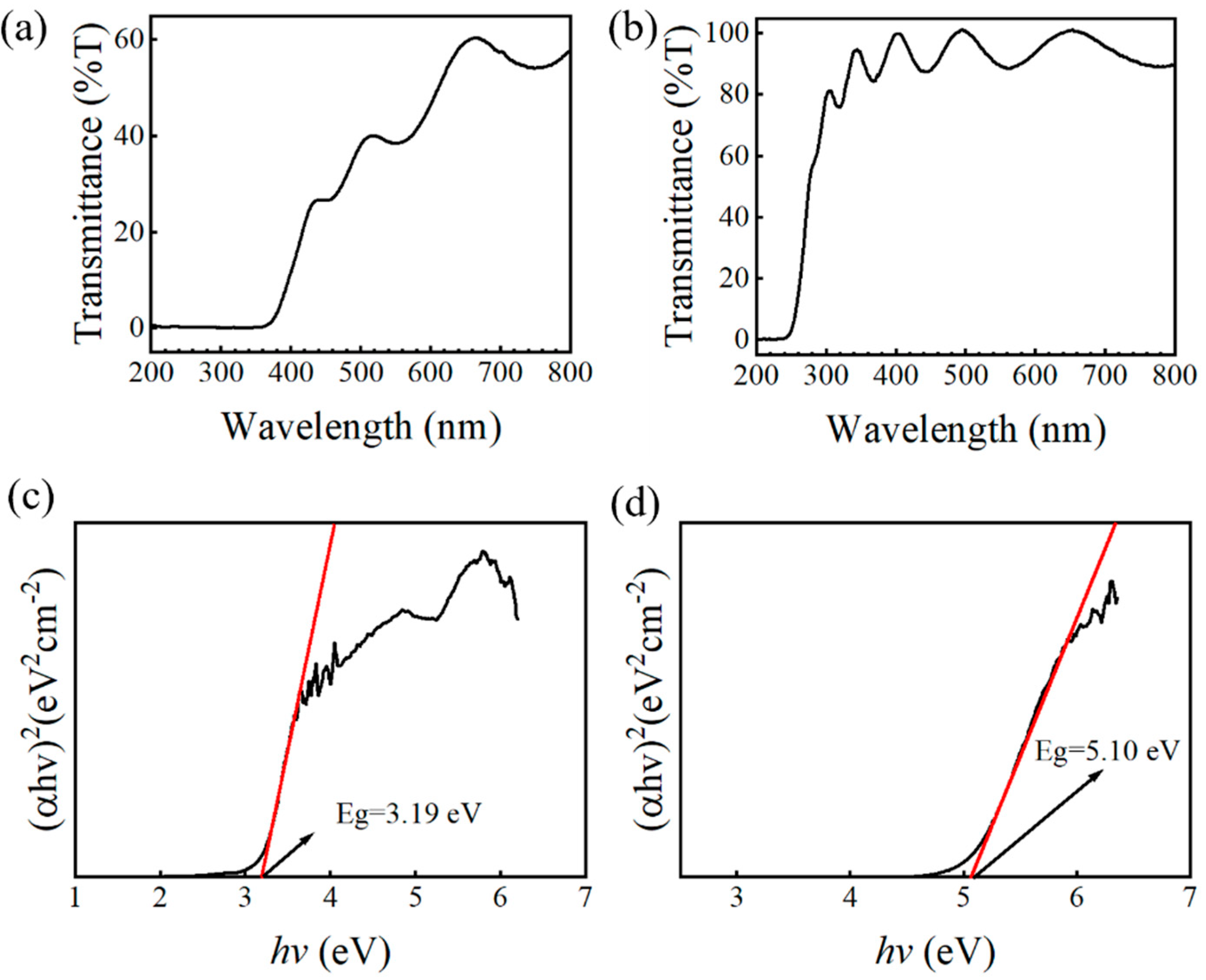
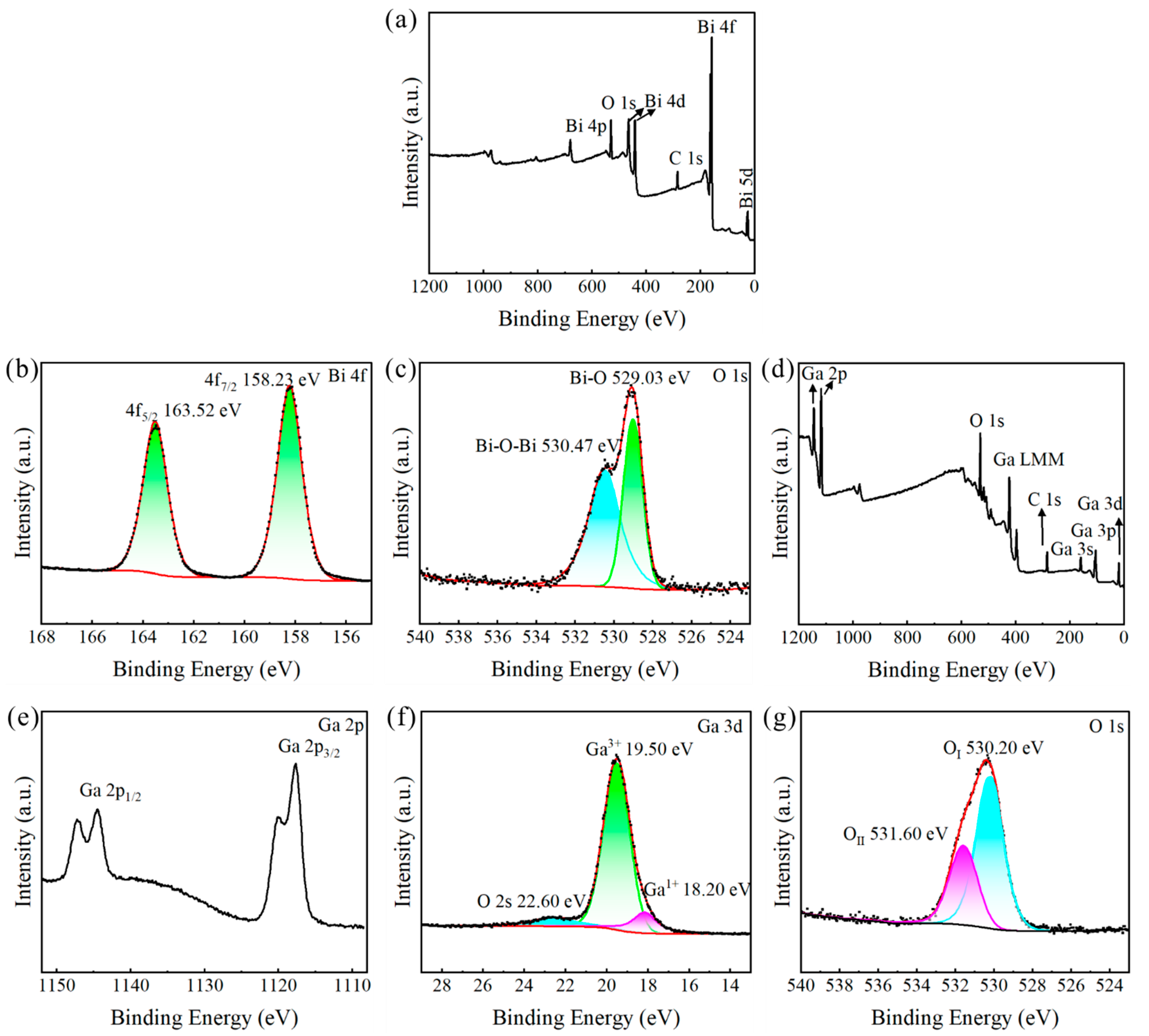
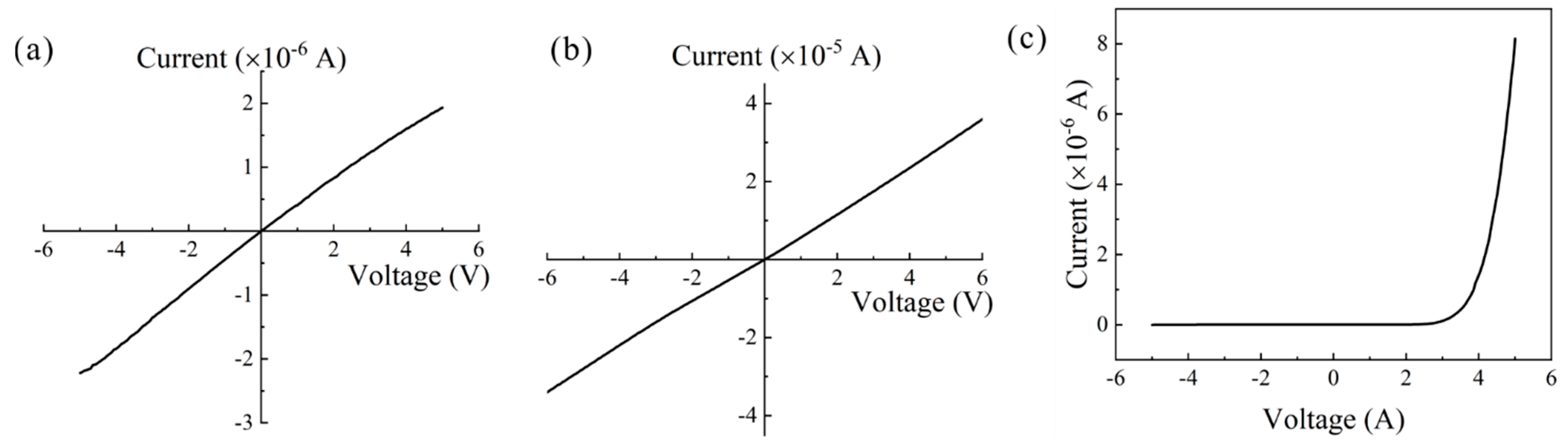
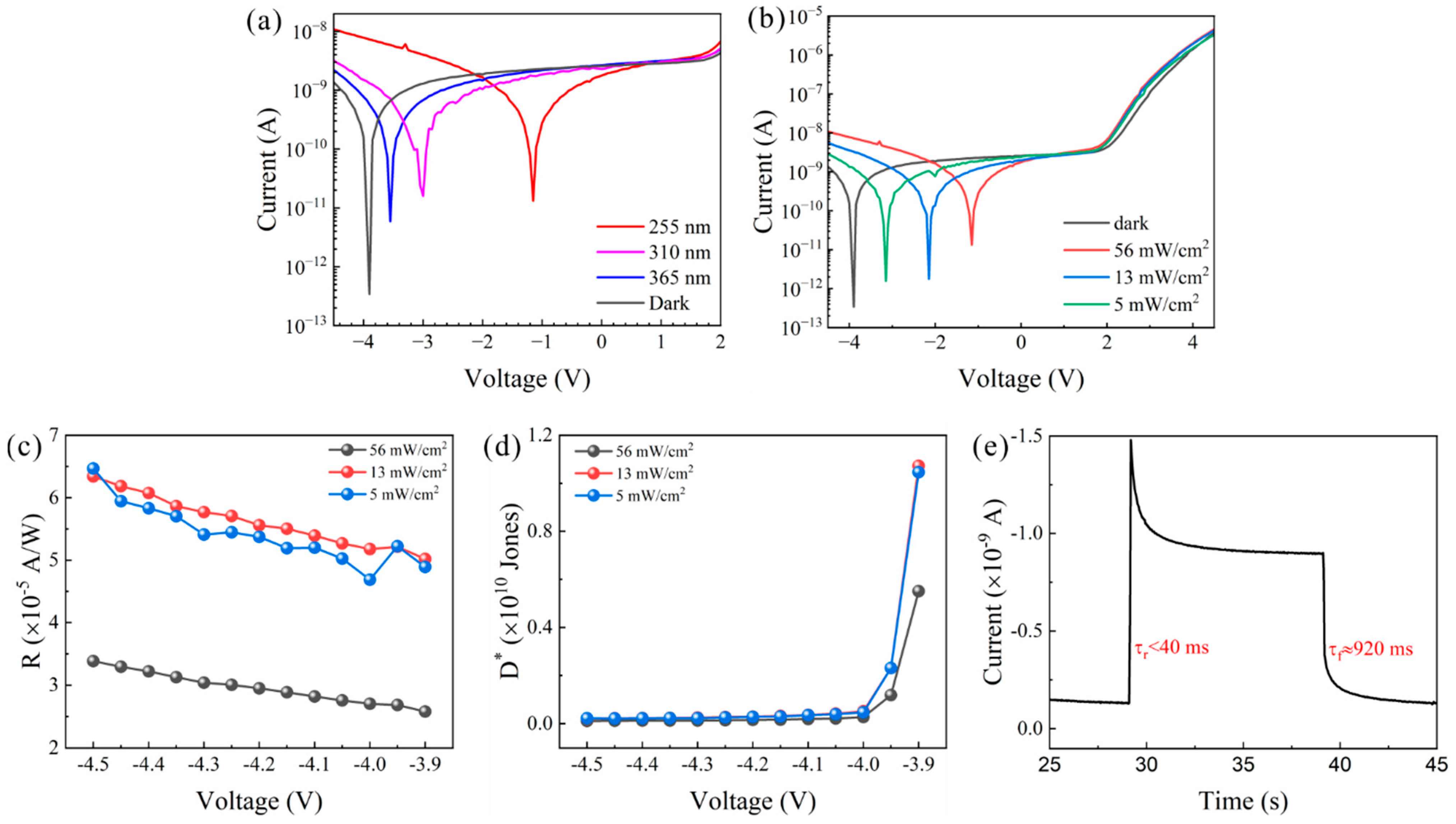
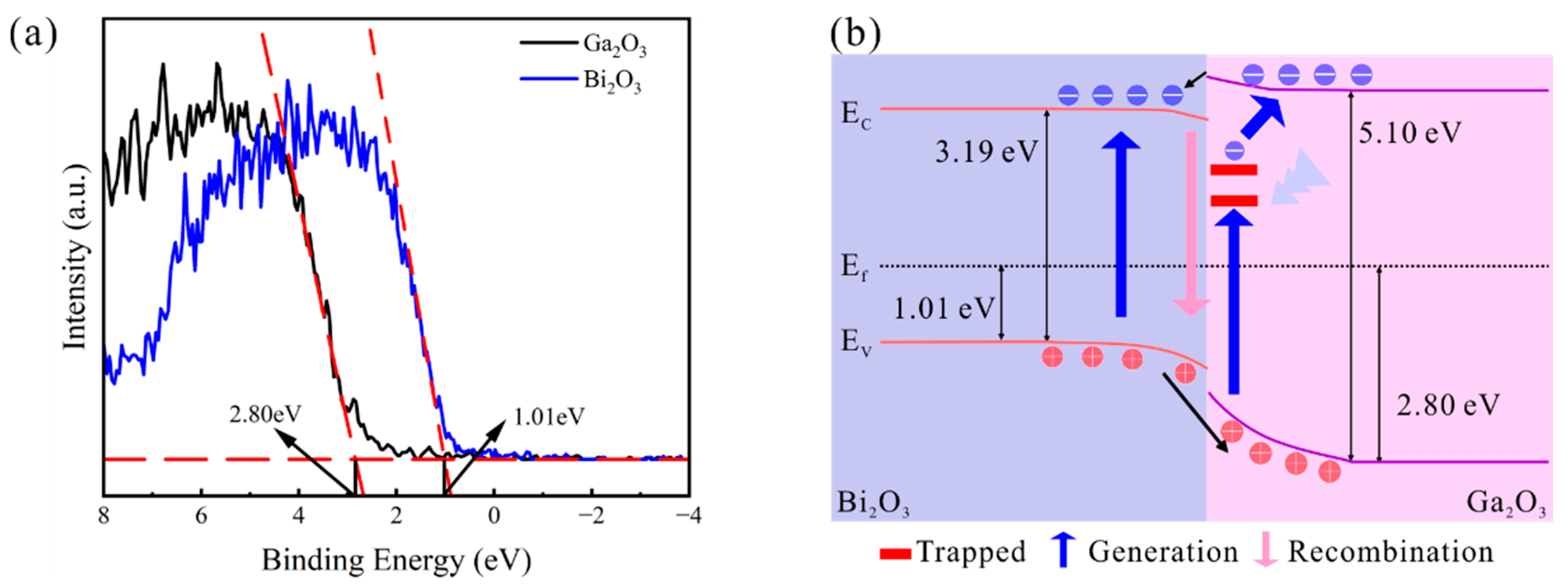
3. Results and Discussion

Figure 1a shows the schematic illustration of the Bi2O3/Ga2O3 heterojunction photodetector, where the ITO electrodes are located on the top and bottom planes of the Bi2O3/Ga2O3 composite films. As shown in Figure 1b, the SEM image presents a typical sandwich structure, which reveals that the fabricated heterojunction is consistent with our design, and the thickness of bottom ITO electrode, Bi2O3 layer, Ga2O3 layer, and top ITO electrode are 110, 340, 140, and 190 nm, respectively. Further, it clearly shows that the films are dense and uniform. The XRD spectra of the as-synthesized samples, Bi2O3, Ga2O3, and 800 °C annealed Ga2O3 films, are displayed in Figure 1c,d. The XRD patterns of Bi2O3 film showed diffraction peaks that matched the PDF#71-2274, suggesting the formation of α phase Bi2O3. However, the relatively broad full width at half maximum (FWHM) of the diffraction peaks indicates that the crystallization quality of the Bi2O3 thin film is deficient. This phenomenon suggests that the thin film likely contains a substantial number of polycrystalline structures, which may account for the observed broadening of the FWHM. It can be observed that the as-deposited Ga2O3 film with 800 °C annealing shows diffraction peaks at 2θ values of 30°, 31.7°, 37.4°, and 64.7°, corresponding to the crystal plane indices of β-Ga2O3 (PDF # 43-1012) at (400), (002), (401), and (512), respectively. The as-deposited Ga2O3 film without annealing does not exhibit significant peaks, indicating that the Ga2O3 thin film is amorphous. This suggests that the amorphous Ga2O3 transforms into β-Ga2O3 upon annealing. Previous research has proven that Ga2O3 material synthesized by the RF magnetron sputtering method at RT demonstrates an amorphous structure [34,35].
Optical transmittance measurements, including transmittance ratio and optical bandgap, are carried out to evaluate the optical parameters of Bi2O3 and Ga2O3 films. The transmittance of the Bi2O3 and Ga2O3 films is investigated by a UV–Vis spectrophotometer, as shown in Figure 2a,b. The Bi2O3 film shows a transmittance value less than 60% in the wavelength range from 200 to 800 nm. Obviously, the Ga2O3 film has an average transmittance of over 80% and shows great absorption at wavelengths less than 280 nm. Commonly, for direct bandgap semiconductor material, the optical bandgap (Eg) can be estimated using the Tauc plots [36]. The estimated bandgap (Eg) and absorption coefficient (α) satisfy the following equation:
)2 = B (Eg)
where is the energy of the incident photons, and B is the absorption edge width parameter. The (αhν)2 versus Tauc plot of Bi2O3 and Ga2O3 films is presented in Figure 2c,d. Utilizing the Tauc method, the optical bandgap is determined through extrapolation of the linear portion of the plot, with the intercept on the photon energy axis serving as the Eg. The values of the Ga2O3 and Bi2O3 films were estimated to be 5.10 and 3.19 eV, respectively.
XPS spectra of the samples with the fitted peaks based on Gaussian fitting analysis are shown in Figure 3, which are used to explore the bonding states of Bi2O3 and Ga2O3 films. Figure 3a depicts the XPS survey spectra of Bi2O3, showing the central energy level positions of Bi 4p, Bi 4d, Bi 4f, Bi 5d, and O 1s. The C 1s peak in the spectra originates from the hydrocarbons in the air. Figure 3b shows high-resolution spectrum of Bi 4f; the banding energies of Bi 4f7/2 and Bi 4f5/2 are located at 158.23 and 163.52 eV, respectively, which correspond to the Bi3+ in α-Bi2O3 [19,37]. The banding energies of O 1s are located at 529.03 and 530.47 eV, attributable to Bi-O and Bi-O-Bi, respectively, as shown in Figure 3c [18,19]. Figure 3d depicts the XPS survey spectra of Ga2O3. Figure 3e presents the high-resolution spectrum of Ga 2p; it is found that both Ga 2p3/2 and 2p1/2 exhibit two peaks, which may be due to the coexistence of multiple crystal phases in the sample. The Ga 3d high-resolution spectrum shown in Figure 3f reveals two fitted peaks, corresponding to the binding energies of Ga3+ and Ga+. The Ga3+ peak is associated with Ga3+ ions in Ga2O3, while the Ga+ peak indicates the presence of gallium in a sub-stoichiometric ratio, suggesting an oxygen deficiency in the material that leads to gallium adopting a lower oxidation state, and the weak peak on the left is attributed to the O 2s signal [38]. Figure 3g presents the O 1s high-resolution spectrum of the Ga2O3 thin film, consisting of two fitted peaks. The peak at 530.2 eV (OI) corresponds to the O-Ga bond, while the peak at 531.6 eV (OII) is attributed to the surface-oxygen defects [38,39,40]. The intensity ratio of OII/(OII + OI) is 35.0%, indicating a significant number of oxygen vacancies in the Ga2O3 thin film.
To confirm the contact type between Bi2O3 and the ITO electrode, as well as between Ga2O3 and the ITO electrode, I–V testing was conducted, and the results are shown in Figure 4a,b. The I–V characteristics of both Bi2O3–ITO and Ga2O3–ITO exhibit a linear behavior, suggesting the formation of a reliable ohmic contact between the semiconductor functional materials and the ITO electrode. Figure 1a shows the I–V test schematic diagram of the Bi2O3/Ga2O3 heterojunction, where the positive and negative poles are connected to the bottom and top ITO electrodes, respectively. Under dark conditions, the I–V characteristic plot of Bi2O3/Ga2O3 heterojunction exhibits a typical rectifying behavior, as shown in Figure 4c, suggesting that a p-n junction is formed in the contact interface of Bi2O3 and Ga2O3 layers. The Bi2O3/Ga2O3 heterojunction shows a high rectification ratio of 2.72 × 10³ under the bias of +4.5/−4.5 V, and an extremely low dark current (0.34 pA @ − 3.9 V), with a highest ON/OFF of 1.07 × 10⁷ (4.5/−3.9 V).
To investigate the UV response performance of Bi2O3/Ga2O3 heterojunction photodetectors, we characterized their I–V characteristics under UV illumination at wavelengths of 255, 310, and 365 nm with a light intensity of 56 mW/cm2, as displayed in Figure 5a. During the experiments, the UV light was incident from the Ga2O3 side to ensure accurate experimental results. The results show that the Bi2O3/Ga2O3 heterojunction photodetector responds to 255, 310, and 365 nm UV light. To better reflect the device’s response capability to UV light, we calculated the photo-to-dark-current ratio (PDCR), responsivity (R), and detectivity (D*) of the device. The PDCR, R, and D* can be expressed by the following equations [34]:
PDCR = I photo I dark I dark
R = I photo I dark P λ S
D * = R S 2 q I dark
where Iphoto is the photocurrent, Idark is the dark current, Pλ is the light power density, S is the effective illuminated area of 1.96 × 10⁻³ cm2, and q is the electron charge. Compared with 255 nm, the fabricated photodetector exhibits a weaker UV response to 310 and 365 nm because only the Bi2O3 layer absorbs photons of the corresponding wavelengths. Clearly, under a bias voltage of − 3.9 V, the fabricated heterojunction photodetector reaches a maximum photo-to-dark current ratio value of 2.11 × 10⁴ @ 255 nm, 3.80 × 10³ @ 310 nm, and 1.66 × 10³ @ 365 nm. After calculation, it can be found that the 255 nm/310 nm rejection ratio (R255 nm/R310 nm) of the fabricated photodetector (5.14 @ −4.5 V) is an order of magnitude larger than R255 nm/R365 nm (11.2 @ −4.5 V). Figure 5b presents the I–V characteristic curves of the Bi2O3/Ga2O3 heterojunction photodetector under 255 nm UV illumination at with various light densities, including 5, 13, and 56 mW/cm2. Under a bias voltage ranging from −3.9 to −4.5 V, the photocurrent increases with increasing light intensity. However, the current under forward bias remains almost unchanged. As Figure 5c shows, responsivity increases with the increase in bias voltage due to enhanced separation and collection efficiency of photogenerated carriers. In contrast, detectivity decreases as the bias voltage increases, owing to the rapid rise in dark current once the bias voltage exceeds the current zero voltage, as displayed in Figure 5d. Under 255 nm UV illumination at 5, 13, and 56 mW/cm2, the fabricated photodetector shows the highest R and D* values of 3.38 × 10⁻⁵, 6.34 × 10⁻⁵, and 6.47 × 10⁻⁵ A/W (@−4.5 V), and 5.51 × 10⁹, 1.07 × 10¹⁰, and 1.05 × 10¹⁰ Jones (@−3.9 V), as listed in Table 2.
It should be emphasized that we have observed a fascinating phenomenon in the Bi2O3/Ga2O3 heterojunction. The minimum current (current zero) of the Bi2O3/Ga2O3 heterojunction photodetector devices does not occur at zero bias but at a negative bias, and it shifts towards a more negative bias as the illuminated UV wavelength increases or the light intensity decreases. Similar phenomena have been reported in Ga2O3-based UV detectors and NiOx/PEDOT:PSS heterojunction solar cells [41,42,43]. The literature has reported that a dipole layer at the interface may result in a notable vacuum level shift, thereby altering the voltage at the current zero for the I–V curves [44]. The formation of the dipole layer at the interface typically results from either the p-n heterojunction or the presence of defect states. The XRD and XPS analysis results reveal that the Bi2O3 and Ga2O3 films contain a large number of oxygen vacancy defects. Therefore, in the Bi2O3/Ga2O3 heterojunction, the shift of the I–V curve is mainly due to the two factors mentioned above. Under UV light illumination, electrons in the valence band of Bi2O3 films are excited to the conduction band, resulting in a change in carrier concentration. This, in turn, causes the redistribution of charges at the heterojunction interface, leading to a change in the dipole layer. Additionally, defects in the heterojunction interface may be excited by absorbed photon energy, further affecting the characteristics of the dipole layer. Therefore, compared with UV illumination conditions, the device shows a higher shift of current zero under dark conditions.
Response time is a key parameter of photodetectors, reflecting how quickly they can respond to changes in optical signals. As shown in Figure 5, the response time can be determined from the current–time (I–T) characteristic curves, including response and recovery processes, i.e., rise time (τr, 10–90%) and fall time (τf, 90–10%). The Bi2O3/Ga2O3 heterojunction photodetector device has a fast response speed, with the rise and fall time of <40 ms and 920 ms. It is important to note that the time resolution of the photoresponsive testing system is 40 ms, indicating that the rise time of the device is faster than 40 ms. Additionally, the device exhibits a current spike at the moment of switching the 255 nm UV on and off, which may be due to the light-induced pyroelectric effect. The literature reports that wurtzite ZnO exhibits pyroelectric potential under light illumination due to its non-centrosymmetric crystal structure [45,46,47]. In our results, the sharp rising edge in the Bi2O3/Ga2O3 heterojunction photodetector is attributed to the non-centrosymmetric crystal structure of the Bi2O3 film. Table 3 compares the critical parameters of Bi2O3- or Ga2O3-based UV photodetectors. The Bi2O3/Ga2O3 heterojunction photodetector, although not showing significant advantages in responsivity and detectivity, clearly exhibits a certain superiority in response speed. Notably, Bi2O3-based photodetectors with excellent performance are predominantly constructed from quasi-one-dimensional materials, which poses great challenges for large-area controllable deposition. Similarly, Ga2O3-based photodetectors rely on complex or costly fabrication techniques, resulting in high expenses for large-area preparation. Therefore, UV photodetectors based on Bi2O3 heterojunction thin films hold significant potential for rapid response and large-area applications.
Figure 6a presents the XPS valence band spectra of Bi2O3 and Ga2O3 films, in which the valence band maxima (VBM) positions were determined by extrapolating the valence band edge to the baseline. The calculated energy separations between the Fermi level and VBM are 1.01 eV for Bi2O3 and 2.80 eV for Ga2O3, respectively. Figure 6b shows energy band diagrams that explain the UV detection performance. The bandgap of Ga2O3 (5.10 eV) is larger than the energy of 255 nm UV light, whereas Bi2O3 has the opposite relationship. Therefore, with 255 nm UV light illumination on the device, the Bi2O3 in the bottom layer preferentially absorbs the light and generates photogenerated carriers. Furthermore, amorphous Ga2O3 contains a large number of defect states and impurity levels within its bandgap. These intermediate states provide lower energy levels, allowing electrons from the valence band to be excited into these defect states by absorbing 255 nm photons. Subsequently, the electrons can be further excited into the conduction band through thermal excitation or multiphoton processes. Under ultraviolet irradiation, photogenerated electron–hole pairs primarily form in the space-charge region. With reverse bias, the conduction band of Bi2O3 shifts upward, and that of Ga2O3 shifts downward, reducing band alignment mismatch. This enhances carrier movement and charge collection at the electrodes. Increasing light power density generates more carriers, while a forward bias reduces the space-charge region width, making carriers less sensitive to changes in light intensity.

4. Conclusions

In summary, all-oxide heterojunction and its UV response performance based on magnetron-sputtering-grown Bi2O3 and Ga2O3 thin films were reported. The structural characterization reveals α phase Bi2O3 and Ga2O3 shows polycrystalline structures. Furthermore, the Bi2O3/Ga2O3 heterojunction shows the highest ON/OFF ratio of 1.07 × 10⁷, and the photodetector shows a high PDCR of 2.11 × 10⁴ and a fast response speed of <40 ms rise time and 920 ms fall time. It is shown that Bi2O3/Ga2O3 heterojunction has potential for application in UV detection.

Author Contributions

Conceptualization, X.C. and F.W.; formal analysis, X.C. and F.W.; funding acquisition, X.C., Z.C. and L.W.; investigation, F.W., J.G., Q.Z. and L.W.; methodology, F.W., J.G. and Q.Z.; supervision, Z.C.; writing—original draft, X.C.; writing—review and editing, L.W. All authors discussed and analyzed the results. All authors have read and agreed to the published version of the manuscript.

Funding

The work is supported by Science and Technology Development Program of GuangXi (Grant No. GuiKe AD23026169), Natural Science Key Project in Scientific Research Foundation for Universities of Education Department of Anhui Province (Grant No. 2024AH051896), Startup Foundation for Doctoral Scientific Research of Wannan Medical College (Grant No. WYRCQD2023021), and National Natural Science Foundation of China (Grant No. 51862031).

Data Availability Statement

Data is contained within the article.

Conflicts of Interest

The authors declare no conflicts of interest.

References

  1. Ji, X.; Yuan, Y.; Yin, X.; Yan, S.; Xin, Q.; Song, A. High-performance thin-film transistors with sputtered IGZO/Ga2O3 heterojunction. IEEE Trans. Electron Devices 2022, 69, 6783–6788. [Google Scholar] [CrossRef]
  2. Lei, W.; Dang, K.; Zhou, H.; Zhang, J.; Wang, C.; Xin, Q.; Alghamdi, S.; Liu, Z.; Feng, Q.; Sun, R.; et al. Proposal and simulation of Ga2O3 MOSFET With PN heterojunction structure for high-performance E-mode operation. IEEE Trans. Electron Devices 2022, 69, 3617–3622. [Google Scholar] [CrossRef]
  3. Liao, C.; Lu, X.; Xu, T.; Fang, P.; Deng, Y.; Luo, H.; Wu, Z.; Chen, Z.; Liang, J.; Pei, Y.; et al. Optimization of NiO/β-Ga2O3 heterojunction diodes for high-power application. IEEE Trans. Electron Devices 2022, 69, 5722–5727. [Google Scholar] [CrossRef]
  4. Guo, J.; Li, S.; Cui, Y.; Zhou, Y.; Guo, W.; Hu, Y.; Xing, Y.; Zhou, Y.; Liu, F. Low-cost tin oxide transparent conductive films for silicon heterojunction solar cells. Adv. Funct. Mater. 2024, 34, 2407273. [Google Scholar] [CrossRef]
  5. Zhu, X.; Wu, Y.; Pan, Z.; Lu, W. Advancements in Ga2O3-based heterojunction ultraviolet photodetectors: Types, fabrication techniques, and integrated materials for enhancing photoelectric conversion efficiency. J. Alloys Compd. 2025, 1010, 177757. [Google Scholar] [CrossRef]
  6. Li, W.; Xu, Z.; Yan, Y.; Gao, Q.; Song, Y.; Wang, J.; Zhang, M.; Xue, J.; Xu, S.; Ding, Y.; et al. Enhancing conductivity in silicon heterojunction solar cells with silver nanowire-assisted Ti3C2Tx MXene electrodes for cost-effective and scalable photovoltaics. Small 2024, 20, 2406397. [Google Scholar] [CrossRef]
  7. Chen, X.; Liu, K.; Zhang, Z.; Wang, C.; Li, B.; Zhao, H.; Zhao, D.; Shen, D. Self-powered solar-blind photodetector with fast response based on Au/β-Ga2O3 nanowires array film schottky Junction. ACS Appl. Mater. Interfaces 2016, 8, 4185–4191. [Google Scholar] [CrossRef]
  8. Lee, S.H.; Kim, S.B.; Moon, Y.-J.; Kim, S.M.; Jung, H.J.; Seo, M.S.; Lee, K.M.; Kim, S.-K.; Lee, S.W. High-Responsivity Deep-Ultraviolet-Selective Photodetectors Using Ultrathin Gallium Oxide Films. ACS Photonics 2017, 4, 2937–2943. [Google Scholar] [CrossRef]
  9. Chen, M.; Zhao, B.; Hu, G.; Fang, X.; Wang, H.; Wang, L.; Luo, J.; Han, X.; Wang, X.; Pan, C.; et al. Piezo-phototronic effect modulated deep UV photodetector based on ZnO-Ga2O3 heterojuction microwire. Adv. Funct. Mater. 2018, 28, 1706379. [Google Scholar] [CrossRef]
  10. Li, Z.; Yan, T.; Fang, X. Low-dimensional wide-bandgap semiconductors for UV photodetectors. Nat. Rev. Mater. 2023, 8, 587–603. [Google Scholar] [CrossRef]
  11. Suchikova, Y.; Nazarovets, S.; Popov, A.I. Ga2O3 solar-blind photodetectors: From civilian applications to missile detection and research agenda. Opt. Mater. 2024, 157, 116397. [Google Scholar] [CrossRef]
  12. Chen, J.; Ouyang, W.; Yang, W.; He, J.H.; Fang, X. Recent progress of heterojunction ultraviolet photodetectors: Materials, integrations, and applications. Adv. Funct. Mater. 2020, 30, 1909909. [Google Scholar] [CrossRef]
  13. Liu, Z.; Liu, Y.; Wang, X.; Li, W.; Zhi, Y.; Wang, X.; Li, P.; Tang, W. Energy-band alignments at ZnO/Ga2O3 and Ta2O5/Ga2O3 heterointerfaces by X-ray photoelectron spectroscopy and electron affinity rule. J. Appl. Phys. 2019, 126, 045707. [Google Scholar] [CrossRef]
  14. Ren, S.; Gao, S.; Lu, H.; Rong, P.; Zhang, X.; Li, L.; Jiao, S.; Wang, D.; Zhang, Y.; Wang, J. A facile template-assisted synthesis of large-scale Bi2O3 nanotube arrays for self-powered UV photodetector. Appl. Surf. Sci. 2022, 590, 153049. [Google Scholar] [CrossRef]
  15. Li, J.-h.; Ren, J.; Hao, Y.-j.; Zhou, E.-p.; Wang, Y.; Wang, X.-j.; Su, R.; Liu, Y.; Qi, X.-h.; Li, F.-t. Construction of β-Bi2O3/Bi2O2CO3 heterojunction photocatalyst for deep understanding the importance of separation efficiency and valence band position. J. Hazard. Mater. 2021, 401, 123262. [Google Scholar] [CrossRef]
  16. Ren, S.; Gao, S.; Zhang, M.; Rong, P.; Lu, H.; Li, T.; Jiao, S.; Zhang, Y.; Wang, J. A simple solution synthesis of massive 2D triangular Bi2O3 nanosheets for self-powered UV photodetection. Opt. Mater. 2023, 135, 113307. [Google Scholar] [CrossRef]
  17. Chen, Z.; Cao, X.; Huang, Y.; Zhang, S.; Pan, W.; Deng, W. Preparation of Ti-doped ZnO/Bi2O3 nanofilm heterojunction and analysis of microstructure and photoelectric properties. Crystals 2023, 13, 264. [Google Scholar] [CrossRef]
  18. Liu, G.; Li, S.; Lu, Y.; Zhang, J.; Feng, Z.; Li, C. Controllable synthesis of α-Bi2O3 and γ-Bi2O3 with high photocatalytic activity by α-Bi2O3→γ-Bi2O3→α-Bi2O3 transformation in a facile precipitation method. J. Alloys Compd. 2016, 689, 787–799. [Google Scholar] [CrossRef]
  19. Meng, L.; Xu, W.; Zhang, Q.; Yang, T.; Shi, S. Study of nanostructural bismuth oxide films prepared by radio frequency reactive magnetron sputtering. Appl. Surf. Sci. 2019, 472, 165–171. [Google Scholar] [CrossRef]
  20. Bera, K.K.; Majumdar, R.; Chakraborty, M.; Bhattacharya, S.K. Phase control synthesis of α, β and α/β Bi2O3 hetero-junction with enhanced and synergistic photocatalytic activity on degradation of toxic dye, Rhodamine-B under natural sunlight. J. Hazard. Mater. 2018, 352, 182–191. [Google Scholar] [CrossRef]
  21. Wu, J.; Wang, F.; Li, H.; Yang, S.; Li, P.; Zhao, Y.; Li, Y.; Zhai, T. Epitaxial growth of 2D ultrathin metastable γ-Bi2O3 flakes for high performance ultraviolet photodetection. Small 2021, 18, 2104244. [Google Scholar] [CrossRef] [PubMed]
  22. Praveen, S.; Veeralingam, S.; Badhulika, S. A flexible self-powered UV photodetector and optical UV filter based on β-Bi2O3/SnO2 quantum dots schottky heterojunction. Adv. Mater. Interfaces 2021, 8, 2100373. [Google Scholar] [CrossRef]
  23. Majumder, S.; Gu, M.; Kim, K.H. Effect of annealing of β-Bi2O3 over enhanced photoelectrochemical performance. Mater. Sci. Semicond. Process. 2022, 141, 106439. [Google Scholar] [CrossRef]
  24. Higashiwaki, M.; Sasaki, K.; Kuramata, A.; Masui, T.; Yamakoshi, S. Development of gallium oxide power devices. Phys. Status Solidi A 2013, 211, 21–26. [Google Scholar] [CrossRef]
  25. Green, A.J.; Speck, J.; Xing, G.; Moens, P.; Allerstam, F.; Gumaelius, K.; Neyer, T.; Arias-Purdue, A.; Mehrotra, V.; Kuramata, A.; et al. β-Gallium oxide power electronics. APL Mater. 2022, 10, 029201. [Google Scholar] [CrossRef]
  26. Qian, Y.P.; Guo, D.Y.; Chu, X.L.; Shi, H.Z.; Zhu, W.K.; Wang, K.; Huang, X.K.; Wang, H.; Wang, S.L.; Li, P.G.; et al. Mg-doped p-type β-Ga2O3 thin film for solar-blind ultraviolet photodetector. Mater. Lett. 2017, 209, 558–561. [Google Scholar] [CrossRef]
  27. Wu, C.; Qiu, L.; Li, S.; Guo, D.; Li, P.; Wang, S.; Du, P.; Chen, Z.; Liu, A.; Wang, X.; et al. High sensitive and stable self-powered solar-blind photodetector based on solution-processed all inorganic CuMO2/Ga2O3 pn heterojunction. Mater. Today Phys. 2021, 17, 100335. [Google Scholar] [CrossRef]
  28. Wang, H.; Ma, J.; Li, P.; Li, B.; Xu, H.; Liu, Y. Piezoelectricity enhanced self-powered solar-blind ultraviolet photodetectors based on Ga2O3/ZnO heterojunction. IEEE Electron Device Lett. 2024, 45, 546–549. [Google Scholar] [CrossRef]
  29. Wang, Y.; Zheng, D.; Wang, K.; Yang, Q.; Qian, J.; Zhou, J.; Liu, S.; Yang, D. Lattice mismatch at the heterojunction of perovskite solar cells. Angew. Chem. Int. Ed. 2024, 63, e202405878. [Google Scholar] [CrossRef]
  30. Zhou, J.; Gong, J.; Sheikhi, M.; Dheenan, A.; Wang, Q.; Abbasi, H.; Liu, Y.; Adamo, C.; Marshall, P.; Wriedt, N.; et al. Synthesis and characteristics of a monocrystalline GaAs/β-Ga2O3 p-n heterojunction. Appl. Surf. Sci. 2024, 663, 160176. [Google Scholar] [CrossRef]
  31. Suchikova, Y.; Kovachov, S.; Bohdanov, I.; Drozhcha, D.; Kosogov, I.; Karipbayev, Z.T.; Popov, A.I. Synthesis and characterization of β-Ga2O3/por-GaAs/mono-GaAs heterostructures for enhanced portable solar cells. Phys. Chem. Solid State 2024, 25, 546–552. [Google Scholar] [CrossRef]
  32. Xu, J.; Zheng, W.; Huang, F. Gallium oxide solar-blind ultraviolet photodetectors: A review. J. Mater. Chem. C 2019, 7, 8753–8770. [Google Scholar] [CrossRef]
  33. Alharbi, S.R.; Qasrawi, A.F. Characterization of the Ge/Bi2O3 Interfaces. Mater. Res. 2019, 22, e20180722. [Google Scholar] [CrossRef]
  34. Saikumar, A.K.; Nehate, S.D.; Sundaram, K.B. Review-RF sputtered films of Ga2O3. ECS J. Solid State Sci. Technol. 2019, 8, Q3064–Q3078. [Google Scholar] [CrossRef]
  35. Kumar, S.S.; Rubio, E.J.; Noor-A-Alam, M.; Martinez, G.; Manandhar, S.; Shutthanandan, V.; Thevuthasan, S.; Ramana, C.V. Structure, morphology, and optical properties of amorphous and nanocrystalline gallium oxide thin films. J. Phys. Chem. C 2013, 117, 4194–4200. [Google Scholar] [CrossRef]
  36. Brik, M.G.; Srivastava, A.M.; Popov, A.I. A few common misconceptions in the interpretation of experimental spectroscopic data. Opt. Mater. 2022, 127, 112276. [Google Scholar] [CrossRef]
  37. Yuan, S.; Wang, J.; Zhao, C.; Yue, L.; Ren, X.; Zeng, Z.; Hu, X.; Wu, Y.; He, Y. S-scheme Bi2O3/CdMoO4 hybrid with highly efficient charge separation for photocatalytic N2 fixation and tetracycline degradation: Fabrication, catalytic optimization, physicochemical studies. Sep. Purif. Technol. 2023, 325, 124665. [Google Scholar] [CrossRef]
  38. Lim, H.; Kim, D.; Yeon Cha, S.; Simon Mun, B.; Young Noh, D.; Chol Kang, H. Crystallization and bandgap variation of non-stoichiometric amorphous Ga2O3-x thin films during post-annealing process. Appl. Surf. Sci. 2022, 585, 152771. [Google Scholar] [CrossRef]
  39. Qian, L.-X.; Wu, Z.-H.; Zhang, Y.-Y.; Lai, P.T.; Liu, X.-Z.; Li, Y.-R. Ultrahigh-responsivity, rapid-recovery, solar-blind photodetector based on highly nonstoichiometric amorphous gallium oxide. ACS Photonics 2017, 4, 2203–2211. [Google Scholar] [CrossRef]
  40. Wang, J.; Ji, X.; Yan, Z.; Qi, S.; Liu, X.; Zhong, A.; Li, P. The role of oxygen vacancies in Ga2O3-based solar-blind photodetectors. J. Alloys Compd. 2024, 970, 172448. [Google Scholar] [CrossRef]
  41. Chen, M.; Zhang, Z.; Lv, Z.; Zhan, R.; Chen, H.; Jiang, H.; Chen, J. Polycrystalline Ga2O3 nanostructure-based thin films for fast-response solar-blind photodetectors. ACS Appl. Nano Mater. 2022, 5, 351–360. [Google Scholar] [CrossRef]
  42. Wu, F.; Pathak, R.; Chen, C.; Tong, Y.; Xu, H.; Zhang, T.; Jian, R.; Li, X.; Qiao, Q. Reduced hysteresis in perovskite solar cells using metal oxide/organic hybrid hole transport layer with generated interfacial dipoles. Electrochim. Acta 2020, 354, 136660. [Google Scholar] [CrossRef]
  43. Zhang, C.; Tong, S.W.; Zhu, C.; Jiang, C.; Kang, E.T.; Chan, D.S.H. Enhancement in open circuit voltage induced by deep interface hole traps in polymer-fullerene bulk heterojunction solar cells. Appl. Phys. Lett. 2009, 94, 103305. [Google Scholar] [CrossRef]
  44. Hu, W.; Liu, Y.; Withers, R.L.; Frankcombe, T.J.; Norén, L.; Snashall, A.; Kitchin, M.; Smith, P.; Gong, B.; Chen, H.; et al. Electron-pinned defect-dipoles for high-performance colossal permittivity materials. Nat. Mater. 2013, 12, 821–826. [Google Scholar] [CrossRef]
  45. Wang, Z.; Yu, R.; Pan, C.; Li, Z.; Yang, J.; Yi, F.; Wang, Z.L. Light-induced pyroelectric effect as an effective approach for ultrafast ultraviolet nanosensing. Nat. Commun. 2015, 6, 8401. [Google Scholar] [CrossRef]
  46. Hsiao, C.-C.; Huang, S.-W.; Chang, R.-C. Temperature field analysis for ZnO thin-film pyroelectric devices with partially covered electrode. Sens. Mater. 2012, 24, 421–441. [Google Scholar]
  47. Kumar, M.; Patel, M.; Lee, G.-N.; Kim, J. Light-Induced all-transparent pyroelectric photodetector. ACS Appl. Nano Mater. 2017, 1, 319–324. [Google Scholar] [CrossRef]
  48. Lang, C.; Yu, X.; Tang, H.; Cheng, J.; Meng, X.; Chen, X.; Chen, M.; Li, J.; Li, L. High stability self-powered Bi2O3 based ultraviolet photodetector with p-i-n heterojunction. J. Alloys Compd. 2025, 1024, 180208. [Google Scholar] [CrossRef]
  49. Sun, B.; Sun, W.; Li, S.; Ma, G.; Jiang, W.; Yan, Z.; Wang, X.; An, Y.; Li, P.; Liu, Z.; et al. High-sensitive, self-powered deep UV photodetector based on p-CuSCN/n-Ga2O3 thin film heterojunction. Opt. Commun. 2022, 504, 127483. [Google Scholar] [CrossRef]
  50. Almaev, A.; Tsymbalov, A.; Kushnarev, B.; Nikolaev, V.; Pechnikov, A.; Scheglov, M.; Chikiryaka, A. Self-powered UVC detectors based on α-Ga2O3 with enchanted speed performance. J. Semicond. 2024, 45, 082502. [Google Scholar] [CrossRef]
  51. Almaev, A.; Nikolaev, V.; Yakovlev, N.; Butenko, P.; Tsymbalov, A.; Boiko, M.; Kopyev, V.; Krymov, V.; Kushnarev, B.; Shapenkov, S.; et al. Electroconductive and photoelectric properties of Pt/(100) β-Ga2O3 Schottky barrier diode based on Czochralski grown crystal. J. Vac. Sci. Technol. A 2024, 42, 042802. [Google Scholar] [CrossRef]
  52. Chen, W.-J.; Ma, H.-P.; Gu, L.; Shen, Y.; Yang, R.-Y.; Cao, X.-Y.; Yang, M.; Zhang, Q.-C. Influence of annealing pretreatment in different atmospheres on crystallization quality and UV photosensitivity of gallium oxide films. RSC Adv. 2024, 14, 4543–4555. [Google Scholar] [CrossRef] [PubMed]
Figure 1. (a) The schematic illustration of the Bi2O3/Ga2O3 heterojunction and its UV response testing schematic. (b) The cross-section SEM image of the fabricated heterojunction. The XRD pattern of the as-deposited Bi2O3 film (c) and Ga2O3 film (d).
Crystals 15 00601 g001
Figure 2. The transmittance of the Bi2O3 (a) and Ga2O3 (b) films, and the corresponding (αhν)2 versus plot of Bi2O3 (c) and Ga2O3 (d) films.
Crystals 15 00601 g002
Figure 3. Survey XPS spectra of Bi2O3 (a) and Ga2O3 (d) films; high-resolution XPS spectra of Bi 4f (b) and O 1s (c) in the Bi2O3 film, and Ga 2p (e), Ga 3p (f), and O 1s (g) in the Ga2O3 films.
Crystals 15 00601 g003
Figure 4. I–V curves of Bi2O3–ITO electrode (a), Ga2O3–ITO electrode (b), and Bi2O3/Ga2O3 heterojunction (c) under dark conditions.
Crystals 15 00601 g004
Figure 5. (a) I–V curves of a Bi2O3/Ga2O3 heterojunction photodetector in darkness and illuminated at 255, 310, and 365 nm UV light. (b) I–V curves of a Bi2O3/Ga2O3 photodetector under 255 nm UV illumination with various light intensities (5, 13, and 56 mW/cm2). Responsivity (c) and detectivity (d) of a Bi2O3/Ga2O3 photodetector as a function of bias voltage under 255 nm UV illumination. (e) Time-dependent photoresponse of a Bi2O3/Ga2O3 photodetector at −3 V bias and 13 mW/cm2 light intensity (@ 255 nm).
Crystals 15 00601 g005
Figure 6. (a) XPS valence band spectra of Bi2O3 and Ga2O3 films, and (b) energy band diagram of Bi2O3/Ga2O3 heterojunction under reverse bias and 255 nm UV light illumination.
Crystals 15 00601 g006
Table 1. Sputtering process parameters of the Bi2O3/Ga2O3 heterojunction.
NameSputtering
Pressure (Pa)
Argon
Flow (sccm)
Sputtering
Power (W)
Time
(Min)
Bi2O30.6406020
Ga2O30.54015060
Table 2. Photoresponse performance of the Bi2O3/Ga2O3 heterojunction photodetector.
Light Intensity
(mW/cm2)
PDCR @−3.9 VR @−4.5 V
(A/W)
D* @−3.9 V
(Jones)
τr/τf
(ms)
56 @ 310 nm3.80 × 1036.58 × 10−69.93 × 10⁸
56 @ 365 nm1.66 × 1033.02 × 10−64.33 × 10⁸
56 @ 255 nm2.11 × 1043.38 × 10−55.51 × 10⁹
13 @ 255 nm9.54 × 1036.34 × 10−51.07 × 10¹⁰<40/920
5 @ 255 nm3.58 × 1036.47 × 10−51.05 × 10¹⁰
Table 3. Comparison of the critical parameters for the Bi2O3- and Ga2O3-based UV photodetector.
StructureFabricate MethodWavelength (nm)Responsivity (A/W)Detectivity (Jones)Rise/Fall Time (ms)Refs
Bi2O3/SnO2 
(nanofibers/
quantum dots)
Electrospinning and hydrothermalUV4.41 × 10−23.18 × 1012100/-
@ 10–90%
[22]
NiO/Bi2O3/TiO2 
(film)
Spin-coating2541.45 × 10−15.50 × 101020.8/21.1
@ 10–90%
[48]
Bi2O3 
(2D flakes)
CVD36564.51.32 × 10130.29/0.87
@ 10–90%
[21]
Bi2O3 
(nanosheets)
hydrothermal365--33/47
@ 0–1/e
[16]
CuSCN/Ga2O3 
(film)
Spin-coating and MOCVD2705.5 × 10−33.81 × 10113.1 × 10−3/0.7 × 10−3
@ 10–90%
[49]
Ga2O3
(film)
HVPE230 or 25430.66.95 × 101518/1.3 × 10−3
@ biexponential
[50]
Ga2O3 
(bulk crystal)
Czochralski21020.49.60 × 101517/27
@ biexponential
[51]
Ga2O3
(film)
ALD2545.8367.72 × 10149.3 × 103/5.2 × 103[52]
Bi2O3/Ga2O3
(film)
RF magnetron sputtering2556.47 × 10−51.05 × 10¹⁰<40/920
@ 10–90%
This work
Disclaimer/Publisher’s Note: The statements, opinions and data contained in all publications are solely those of the individual author(s) and contributor(s) and not of MDPI and/or the editor(s). MDPI and/or the editor(s) disclaim responsibility for any injury to people or property resulting from any ideas, methods, instructions or products referred to in the content.

