Article

The Effect of Spark Current Tuning on the Formation of Cu Nanoparticles Synthesized by Spark Ablation in Nitrogen Atmosphere

1
Institute for Microelectronics and Microsystems, CNR-IMM, Via Monteroni, 73100 Lecce, Italy
2
Mathematics and Physics “E. De Giorgi” Department, University of Salento, Via Monteroni, 73100 Lecce, Italy
*
Authors to whom correspondence should be addressed.
Crystals 2025, 15(7), 587; https://doi.org/10.3390/cryst15070587
Submission received: 20 May 2025 / Revised: 18 June 2025 / Accepted: 19 June 2025 / Published: 21 June 2025
(This article belongs to the Section Inorganic Crystalline Materials)

Abstract

The demand for a “green” approach to the synthesis of nanomaterials is becoming increasingly pressing. In response to this need, we present, for the first time, the use of spark ablation as an environmentally friendly deposition technique to obtain nanoparticles of copper nitride, a material that is gaining increasing attention in the field of photovoltaic advanced technologies. This method involves the ablation of pure copper electrodes in nitrogen atmosphere while a spark current is tuned. The overall result is the co-presence of nitride and oxide nanoparticle agglomerates with different sizes according to the spark current, as confirmed by X-ray diffraction, Raman spectroscopy, X-ray photoelectron spectroscopy and energy-dispersive spectroscopy techniques. Scanning probe microscopy and scanning electron microscopy show an increase in the number and size of nanoparticle agglomerates with an increasing current, while the nanoparticle size is always about sub-10 nm. The findings of this work promote spark ablation as a simple, versatile, cost-effective, environmentally friendly deposition method to obtain nitride-based nanoparticles. Furthermore, it is compatible with many types of materials and substrates, increasing the possible combinations of metals/semiconductors and carrier gas types to obtain completely innovative materials with unique compositions and properties.

1. Introduction

Due to their large surface-to-volume ratio and the size effects of quantum mechanics, nanoparticles (NPs) have potential applications in various fields such as nanoelectronics, sensors and biosensors, non-linear optics, catalysis, hydrogen storage and solar technology [1]. NPs are mainly synthesized through the sol–gel process, but recently, gas-phase methods have been increasingly applied [2]. Gas-phase synthesis has the advantage of high purity due to the absence of liquid solvents, and the higher thermal stability of gases compared to liquids makes the approach very flexible. Moreover, it usually provides crystalline NPs that can have different sizes by tuning the experimental parameters.
One of the most versatile techniques for generating gas-phase NPs is spark ablation, an innovative physical deposition technique that meets the growing need for new and versatile materials with specific properties tuneable in an easy way. In this process, very tiny spots on the surface of metal/semiconductor electrodes are rapidly sublimated into a vapour cloud when a discharge is generated at ambient pressure between two electrodes facing each other, creating high-temperature plasma (about 20,000 °K) [3]. This cloud flow, transported by a carrier gas, travels away from the plasma region towards the deposition area. During this, it rapidly cools down, coalescing into single NPs, and then aggregates/agglomerates through a condensation process. Its strength and versatility lie in three main aspects: the possibility to ablate different metallic/semiconductor materials in the same deposition process, creating completely new and complex alloys, hardly achievable with other techniques; the employment of different deposition configurations (i.e., filtration, impaction) that allow for the coverage of many kinds of substrates (flexible and porous or rigid) with different sizes, according to the application; and the option to operate not only with an inert gas but also in a reactive atmosphere to produce nanostructured compounds (nitrides and oxides). Moreover, it is an eco-friendly process as no chemical precursors are required and no waste is produced [4]. Regarding impaction configuration, it is the most versatile one for two main reasons. First, it allows for the deposition of thicker porous films that are extremely advantageous for specific applications [5]. Second, it can be easily combined with a printer by moving the nozzle in the XY-plane to directly write complex patterns without lithography or masks [6,7]. Being a valid method to create new materials with exclusive compositions, spark ablation represents a challenging route to obtain nanostructured materials, suitable for advanced technology development [8]. With a specific focus on photovoltaic advanced technology and smart futuristic lithium-ion batteries, one of the semiconductors that is attracting the interest of materials scientists is copper nitride [9,10]. Copper nitride is a semiconductor with an indirect bandgap energy of about 1.4 eV, which makes it an ideal material for solar energy conversion [11]. The growing attention towards this compound is also due to its non-toxicity and its cheapness, the fact that it is made of earth-abundant elements, and especially because its bandgap can be easily tuned to meet the suitable absorption properties required for the application [12]. The fabrication of materials at the nanoscale is a hot topic in the photovoltaic systems field because nanostructures can potentially improve the efficiency of devices [13,14]. Spark ablation guarantees not only nanostructure fabrication in an easy and green way but also the low cost of production compared to other technologies [15].
In this work, we present an easy, versatile, and eco-friendly way to synthesize copper nitride NPs by the spark ablation of pure Cu electrodes in nitrogen atmosphere. The influence of the spark current on the morphology, structure, and chemistry of the samples was analysed by using Atomic Force Microscopy (AFM), scanning electron microscopy (SEM), scanning tunnelling microscopy (STM), X-ray diffraction (XRD), Raman spectroscopy, X-ray photoelectron spectroscopy (XPS), and energy dispersive X-ray spectroscopy (EDS). To the best of our knowledge, this is the first work that discusses Cu-N NP deposition by spark ablation, providing a new advantageous route to obtain NPs made of this compound compared to more traditional ones [16] in a safe way and carried out at atmospheric pressure and room temperature.

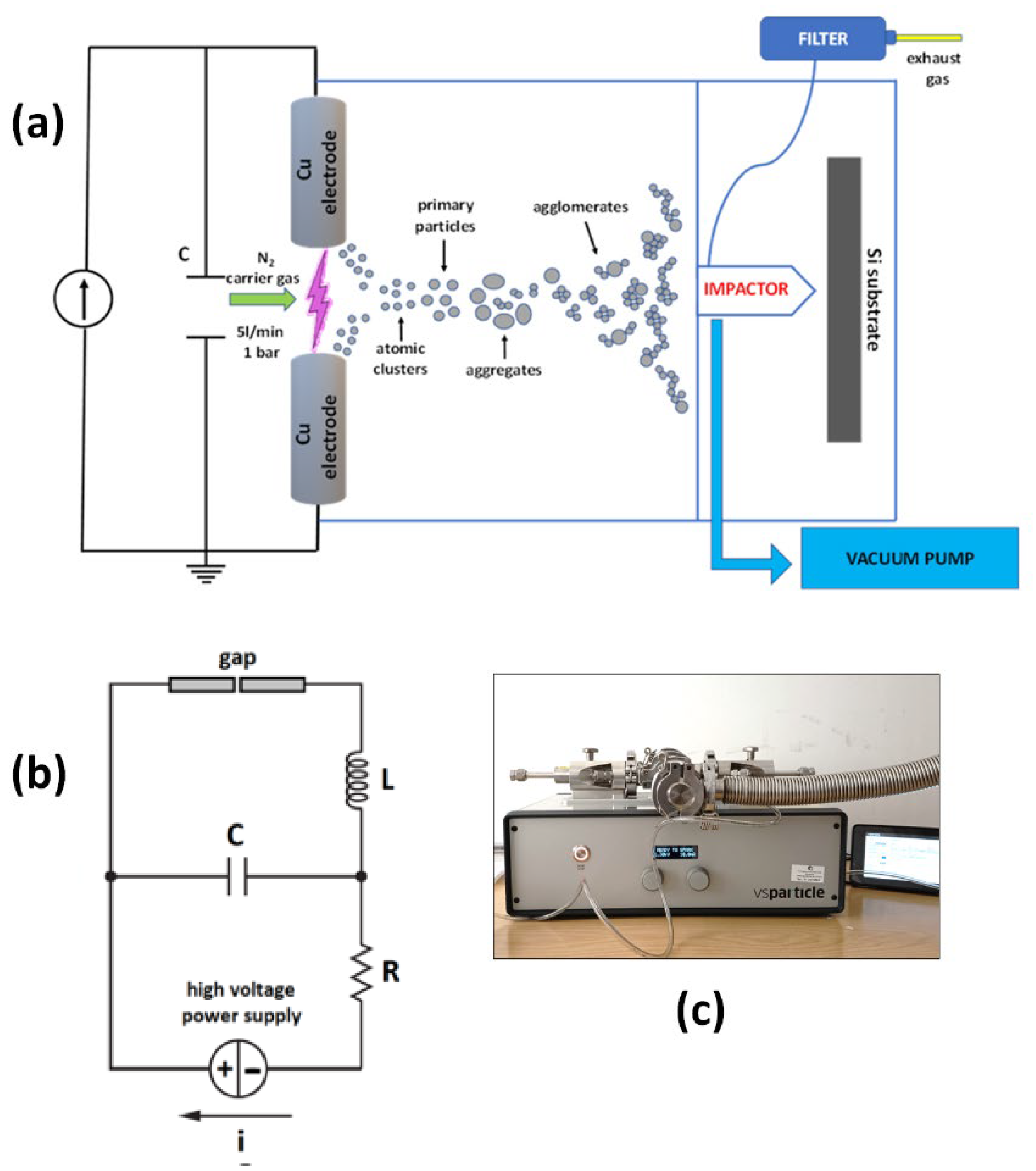
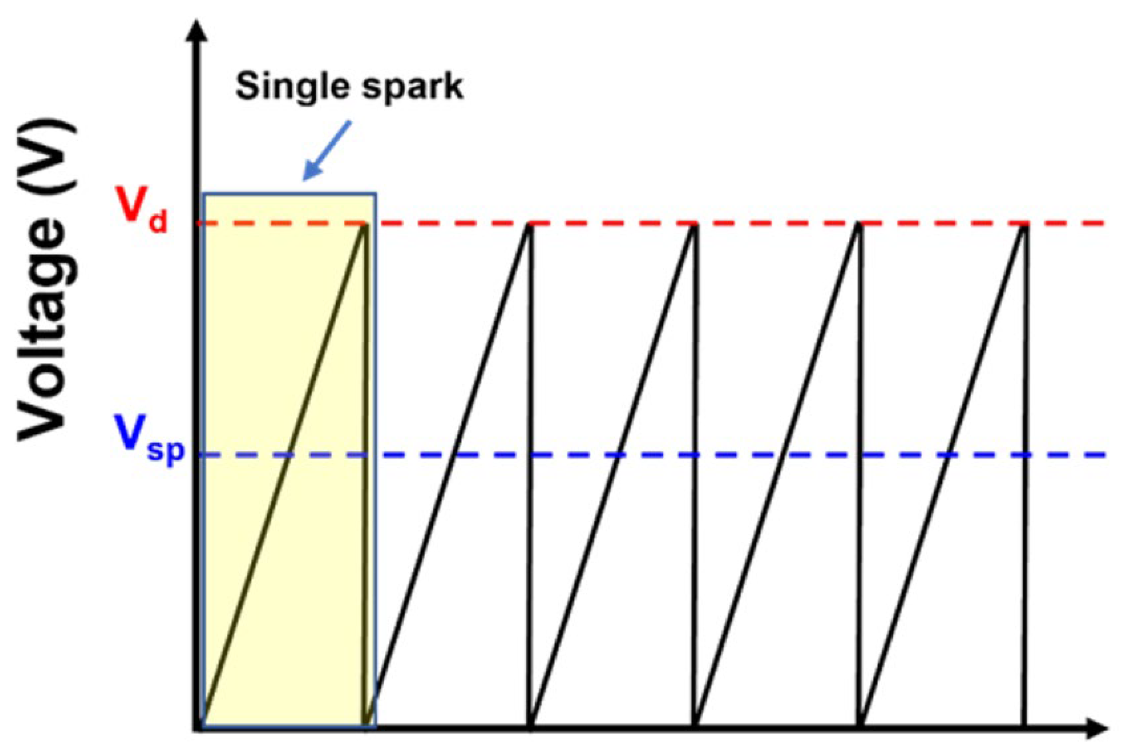
2. Materials and Methods

Copper nitride NPs were deposited on silicon substrate by the spark ablation technique using a VSP G1 nanoparticle generator apparatus (VSParticle, Delft, The Netherlands) arranged in an impaction configuration. It was equipped with two copper electrodes (30 mm long and 6 mm thick cylinders, 99.9% purity) facing each other, with variable distance automatically controlled by a micrometric manipulator, piping to transport the produced metal vapour cloud through a carrier gas flow, a nozzle for the impaction-based transfer of the ablated mass towards the substrate, and a deposition chamber where the substrate was located. Our experiments are conducted by configuring a spark ablation system in a crossflow vacuum-assisted impact deposition setup. In this configuration, the electrical discharge generates an arc between the electrodes, creating plasma that causes the evaporation of the electrode materials. The generated vapour is carried out by the carrier gas (nitrogen in this case) from the electrode region to the deposition chamber where the substrate is placed. The directionality of the vapour flux is caused by the pressure difference between the spark chamber and the deposition chamber where the pump is on. The high-voltage generator is combined with a 25 nF capacitor (C) to collect the charge until discharge occurs at a specific frequency. Before starting the deposition process, nitrogen gas was introduced into the system, flowing for 30 min, both for cleaning the system and stabilizing the gas carrier flux. The processes were conducted at a deposition pressure equal to 1022 mbar in nitrogen gas flow set to 5 L/min. The carrier gas flow mainly influences the particle size distribution, and this almost high value was selected to guarantee the formation of smaller NPs with a size lower than 10 nm deposition [17]. The tuned parameter was the spark current Ispark (5, 7 and 10 mA), which influences the aerosol concentration, while the spark voltage Vsp and the deposition time were kept constant at 1.3 kV (the set-point voltage value) and 300 s, respectively. The deposition conditions are summarized in Table 1.
A schematic of the deposition equipment can be visualized in Figure 1a. The equivalent electrical circuit scheme of the spark generator is shown in Figure 1b. This circuit is simple yet ingenious at the same time. The spark itself acts as a switch and requires no fast-switching electronics. The current source charges capacitance C and a spark occurs when its voltage reaches the gas breakdown value, then the capacitor is discharged, and the process is repeated with a specific frequency. Figure 1c shows a photograph of the VSP-G1 nanoparticle generator employed in this work.
The structure of the samples was investigated by X-ray diffraction (XRD). Broad-scan analyses were performed using a Rigaku SmartLab SE diffractometer (Tokyo, Japan) in pseudo-parallel Bragg–Brentano mode with an incident angle of 0.3°, and the spectra were collected in the 2θ range from 10° to 80°, using Cu Kα radiation (λ = 0.154 nm) at 40 kV and 50 mA. The step size was set to 0.010° and the scan speed was 0.2° min−1.
Further structural information of the nanoaggregates was acquired by Raman spectroscopy. The analyses were performed by means of an InVia spectrometer, Renishaw PLC (Gloucestershire, UK). An Ar+-ion laser working at 514.5 nm was used as the excitation source (25 mW of the maximum output power). All spectra were collected at room temperature in the spectral range of 200–1500 cm−1 and with a resolution of 1.5 cm−1.
The surface topography, morphology, and roughness of the nanoaggregates were investigated by Atomic Force Microscopy (AFM—Nanosurf CoreAFM, manufacturer is Nanosurf AG, Liestal, Switzerland). AFM topography images were acquired in tapping mode, at room temperature and in air environment. Silicon probe tips with chromium–platinum conductive coating (MULTI75-EG, manufacturer is BudgetSensors, Sofia, Bulgaria) were used at the typical resonance frequency of 75 kHz, with a constant force of 3 N/m. The roughness of the samples was determined from the root mean square (RMS) calculated with the commercial Gwyddion 2.68 software.
A CreaTec Fischer variable-temperature ultra-high vacuum (UHV) scanning tunnelling microscope was employed to perform STM measurements at room temperature in UHV (10−10 mbar) using a Pt/Ir tip. Copper NPs were deposited on Au (111)/mica substrate.
For a further characterization of the NPs’ morphology, the samples were loaded into the Cryo-FIB/SEM system (Tescan-Amber, TESCAN Essence Software, Version 1.3.4.0 build 8124). The system is composed of an electron beam and an ion beam that can be employed distinctly for surface observation and ion milling within a single instrument. SEM imaging was conducted in ultra-high-resolution mode, operating at an accelerating voltage of 5 kV and a current of 100 pA. To carry out EDS measurements in the SEM, a low accelerating voltage (2–5 kV) was used to detect the characteristic X-rays of nitrogen present at the surface, associated with copper nitride formation. This approach was chosen to exploit the reduced penetration depth of the electron beam at low voltages, thereby enhancing surface sensitivity and minimizing the contribution from the underlying substrate. However, due to the limited excitation volume and lower X-ray yield at these voltages, this method does not allow for accurate quantitative analysis.
XPS measurements were performed by using a Phoibos150 (Specs) photoelectron spectrometer with a monochromatic Mg Kα source (1253.60 eV) operating at 200 W (15 kV, 15 mA). Base pressure in the analysis chamber was 8 × 10⁻⁹ mbar. The deposited silicon substrate was mounted onto the sample holder by using conductive adhesive tape. Survey scan spectra were acquired utilizing a pass energy of 100 eV and a 1 eV step. High-resolution spectra were acquired using a pass energy of 25 eV and 0.03 eV step. In each case, the analysed area was about 700 μm × 300 μm. The spectra were processed by CasaXPS software Version 2.3.16Dev52. The binding energy scale was referenced to the adventitious C 1s peak (284.8 eV). For the analysis of high-resolution spectra, all peaks were fitted using the Shirley background and GL (30) line shape (a combination of Gaussian 70% and Lorentzian 30%).

3. Results

The XRD patterns of spark-ablated NPs are shown in Figure 2 and they are used to determine the crystalline phase of the nanostructures.
All sample patterns showed peaks attributable to metallic, nitride, and oxide phases that co-exist in the nanosctructured films. The diffraction peak centred at 2θ = 32.9° comes from silicon substrate. The most intense diffraction signal at 2θ = 51.3° is due to the reflection from the metallic Cu (002) planes (JCPDS# 04–0836). Two contributions from the Cu3N nitride phase were detected: a very weak diffraction peak centred at 2θ = 22.6°, ascribable to Cu3N (100), and another more relevant reflection at 2θ = 40° coming from Cu3N (111) planes [18]. An oxide peak was found around 2θ = 31°, attributable to monoclinic CuO (110) crystallites (JCPDS# 01-080-0076).
The presence of an oxide is expected because it is well known that Cu NPs are very susceptible to oxidation and gradually convert to Cu oxides in the presence of air or other oxygen sources [19]. In fact, one of the most common effects during the synthesis of CuxN by various techniques (both chemical and physical) is the presence of O as an impurity embedded in the films [20]. The monoclinic structure of Cu-O is the favourite oxide phase as it is the most stable [21].
With the aim to elucidate the local crystal structure of the samples, Raman spectroscopy was conducted, and the spectra are shown in Figure 3.
The peak detected at around 620 cm−1 can be assigned to the copper nitride phase (the pink box in the Figure), specifically to the stretching mode of a Cu-N bond [22,23,24]. The slight shift towards a lower wavenumber could be attributed to deviation from a stoichiometric compound, i.e., a Cu-rich nitride structure [12]. The Raman peak around 985 cm−1 is attributed to silicon substrate [25]. The band located at around 300 cm−1 is a characteristic vibration of a monoclinic CuO crystal [26], specifically Ag Raman-active mode, confirming the presence of this structure hypothesized by XRD analysis. A peak around 800 cm−1 is also detected, very small at the lowest spark current and more visible at the highest one. It can be attributed to the unintentional formation of Cu(OH)2 on the surface after the exposure of the nitride films in air [27,28]. The broad band around 1100 cm−1 belongs to C-C stretching modes due to surface carbon-based adsorbates from the atmosphere [29]. These results are in good agreement with the XRD analysis.
X-ray photoelectron spectroscopy (XPS) was employed to investigate the surface chemistry. The survey spectrum for a representative as-received sample (10 mA), shown in Figure 4, evidences the spectral signatures attributable to all the expected elements, i.e., Cu, N and O, together with other possible elements detectable on the sample’s surface.
The carbon trace detected in the survey is attributable to the presence of organic contaminants introduced during the handling process or CO2 adsorbed from the atmosphere, as found in the Raman spectra. The high-resolution spectra of C 1s, Cu 2p, O 1s, and N 1s are shown in Figure 5.
The spectrum of the C1s peak (Figure 5a) is fitted by three components with binding energies of 284.8 eV (1), 286.6 eV (2), and 288.6 eV (3). These peaks are assigned to C-C/C–H, C–O–C, and O–C=O groups, respectively. The C-C/C-H group peak position is considered a reference to correct the charging effect of the sample.
Figure 5b depicts the Cu 2p XPS spectrum and the fitting process into sub-peaks. It is generally separated into Cu 2p3/2 and Cu 2p1/2 doublet structures (two peaks) due to the spin–orbit coupling. The binding energy of the main Cu 2p3/2 and Cu 2p1/2 photoemission lines is in correspondence with the ISO calibration standard reference values [30]. Cu 2p3/2 and Cu 2p1/2 are fitted into two sub-peaks. Cu+ 2p3/2 and 2p1/2 signals are located at binding energies of about 932.8 eV and 953.1 eV, respectively, while Cu2+ 2p3/2 and 2p1/2 signals peak at about 933.9 eV and 954.9 eV, respectively [31]. This indicated that the valence of Cu on the surface of the NP film is +1 or +2. The binding energy equal to 932.8 eV is equal to the value reported for Cu3N films [32]. Three satellite peaks are detected, too, indicated by asterisks in the Figure. Two satellites are centred at 940.2 eV and 943.2 eV, and another one at about 961.8 eV, generally due to the “shake up” process when additional electrons are excited to higher energy states [33]. It is worth additionally noting that the copper Auger peak (Cu LMM) reported in the survey is a further indication of the presence of Cu2+ or similarly of CuO presence in the aggregates [30,31,34].
Figure 5c shows the peak fitting of the O 1s high-resolution XPS spectrum. Two sub-peaks are identified under the main peak (at 531.1 eV), located at 529.9 eV (1), attributable to O2- in CuO [35], and at 531.5 eV (2), assignable to the oxygen atoms from the OH- groups on the CuO surface [36].
Figure 5d shows the results of the fitting procedure on the N 1s high-resolution XPS spectrum. The high-resolution N 1s spectrum is fitted by three distinct components centred at 398.7 eV (1), 400.0 eV (2), and 401.6 eV (3), which can be assigned to a Cu–N bond [37], nitrogen dissolved into the copper nitride NP film [38], and N–O bonds [39], respectively.
Table 2 summarizes the results of the fitting procedure for each analysed element.
The surface morphology of the samples was studied by AFM and SEM. Figure 6 depicts the AFM 2D micrographs at different spark currents.
All the deposited nanoparticle layers appear continuous and uniform on the silicon substrate while showing a co-presence of aggregates and smaller particles. The particle aggregates change their dimension according to the current. At the highest Ispark = 10 mA (Figure 6c), their size falls in the interval 100–300 nm, which decreases down to 80–160 nm at 7 mA of spark current (Figure 6b) and reaches the lowest values between 50 nm and 130 nm at the lowest current of 5 mA (Figure 6a). The increase in the current also causes a slight rise in the surface roughness, from 5 nm (at 5 mA) to about 8 nm (at 10 mA). AFM analyses also revealed, for all samples, the presence of spheres (few hundred nm in diameter) and agglomerates (sizes from a few hundred nm to few mm) randomly distributed over their surface (see red and green circles in Figure 6d, respectively, of the sample ablated at a current of 10 mA, taken as representative). They are known as “splashing particles”. By the use of STM, the individual size and size distribution of the particles were better analysed. Figure 7 displays a representative STM image (size scan 100 × 100 nm2, Figure 7a) carried out at a tunnelling current of 60 pA together with a profile section (Figure 7b) corresponding to the white dotted line. The images clearly show how the aggregates are composed of sub-10 nm particles, resulting in an average size equal to (6.6 ± 0.7) nm, confirming the small size of NPs at the selected gas carrier flow.
The morphology images obtained by SEM observations are shown in Figure 8 together with the elemental mappings recorded by EDS analysis for the sample ablated at 10 mA of spark current, taken as representative.
All films appear almost uniform on the silicon substrate, as AFM showed, too. The presence of randomly distributed small self-assembled splashing particles of varying diameters in the range 100–400 nm can be observed, in line with AFM scans. These spheres are evidenced by red circle in the figure, and they have different densities according to the ablation process conditions. Specifically, it decreases by diminishing the spark current. A density of (120 × 104) spheres/mm2 can be counted for the sample deposited at 10 mA of spark current, which decreases down to (60 × 104) spheres/mm2 at 7 mA and finally down to (2 × 10⁴) spheres/mm2 at 5 mA. The origin of these round NPs is not easy to understand as spark discharge is a very complex process. Some authors [18,40] describe two different mechanisms occurring in spark discharge that can form spherical NPs with diameters of several hundred nm. They can be “primary particles”, made exclusively of pure metal from the electrodes, that are formed by the collision of smaller spherical particles and undergo complete coalescence; alternatively, they can form parallel to the evaporation–condensation process by the separation of the material directly from the locally heated electrode surface. For the latter mechanism, the authors observed that the dimension of these large “solidified droplets” range from 100 nm to a few microns and their number is negligible compared to that of NPs. Splashing particles coexist with NP agglomerates whose sizes change with the spark current. In detail, their size varies in the range 1–2 μm at the lowest spark current (Figure 8a), reaching a dimension of 3 μm when the current rises to 7 mA (Figure 8b), and up to 5 μm at the highest set spark current (Figure 8c). Moreover, the agglomerate density increases with the current rising, too. Compared to other aggregate formation, these larger agglomerates were instead formed at a later stage, in proximity of the substrate area, when the temperature dropped below the value that allows rapid coalescence, leading to an irregular shape. Dilution and cooling by the flowing gas take place near the substrate position region, where room temperature can be assumed. In the diluted state, more agglomeration may occur before reaching the substrate, because the time available is orders of magnitude longer than the time in the hot zone before dilution. Further aggregation may occur on the substrate surface. Figure 8c also shows, as an example, an EDS analysis of the sample deposited at 10 mA. The images indicate that the analysed layer is made of copper, nitrogen, and oxygen, suggesting that oxide and nitride are formed. In particular, an analysis of the agglomerate (see the green box) shows signs of both copper and oxygen, rather than nitrogen, as they form at a later stage, close to the substrate area, having plenty of time to oxidize. Nitrogen seems to be placed mainly around particles. In contrast, an EDS analysis of the sphere (see the blue box) shows that it is essentially made up of copper only, confirming the thesis that this type of structure was formed in the first moments after spark discharge.

4. Discussion

The spark ablation of pure copper electrodes in nitrogen atmosphere by tuning the spark current resulted in the deposition of nitride particle agglomerates, together with metallic and oxide ones. This main finding was confirmed by the synergistic roles of the different employed characterization techniques, whose results can be summarized as follows:
-
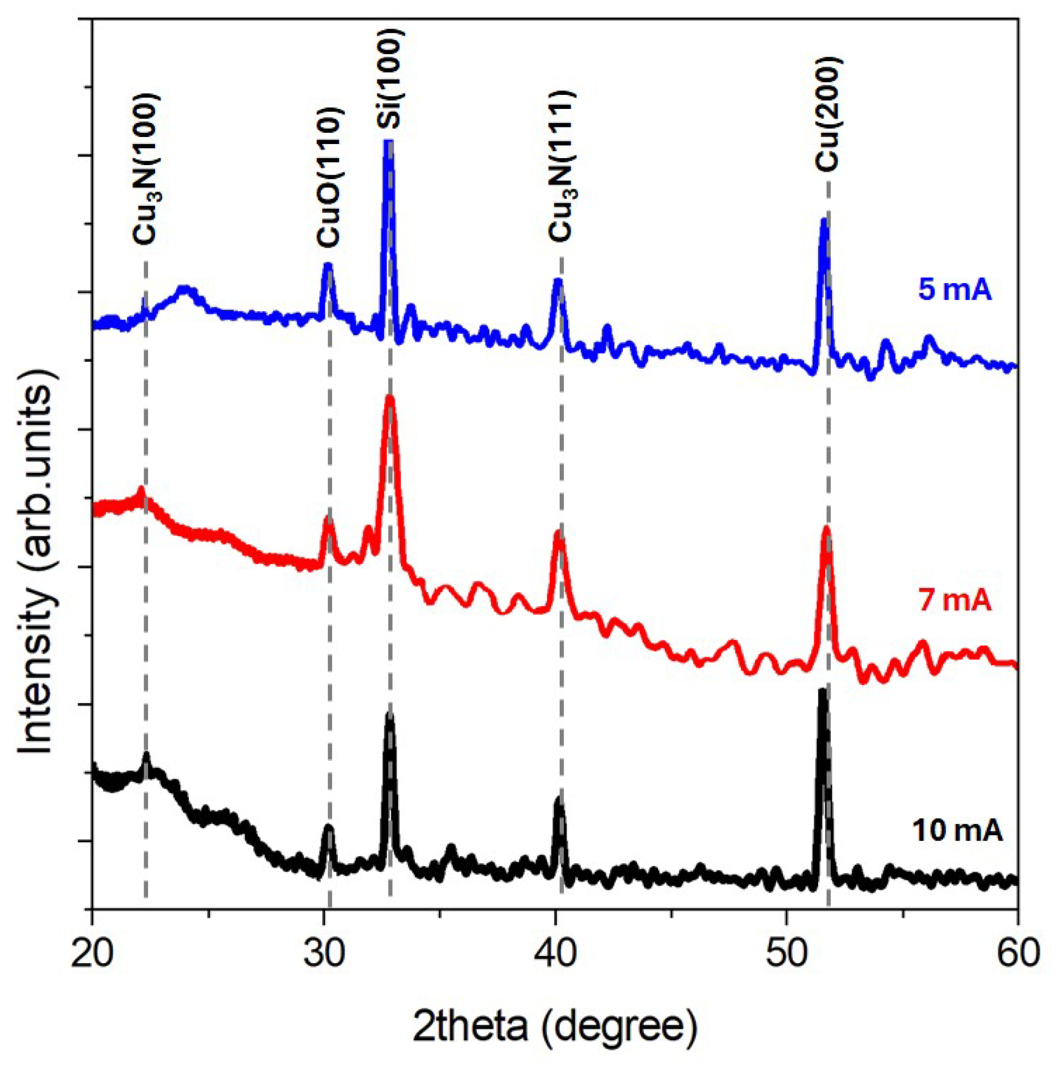
The XRD spectra consist of broad peaks where we assume that nitride and oxide compounds coexist; in particular, two contributions from the Cu3N nitride phase are detected at 2θ = 22.6° (100) and 2θ = 40° (111).
-
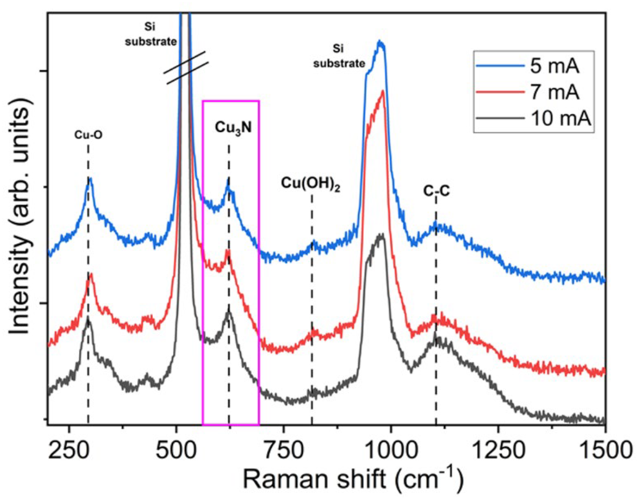
The Raman analysis shows good agreement with the XRD results, recording peaks at a Raman shift assigned to the Cu-N stretching mode and additionally to the characteristic vibration mode of the monoclinic CuO crystal.
-
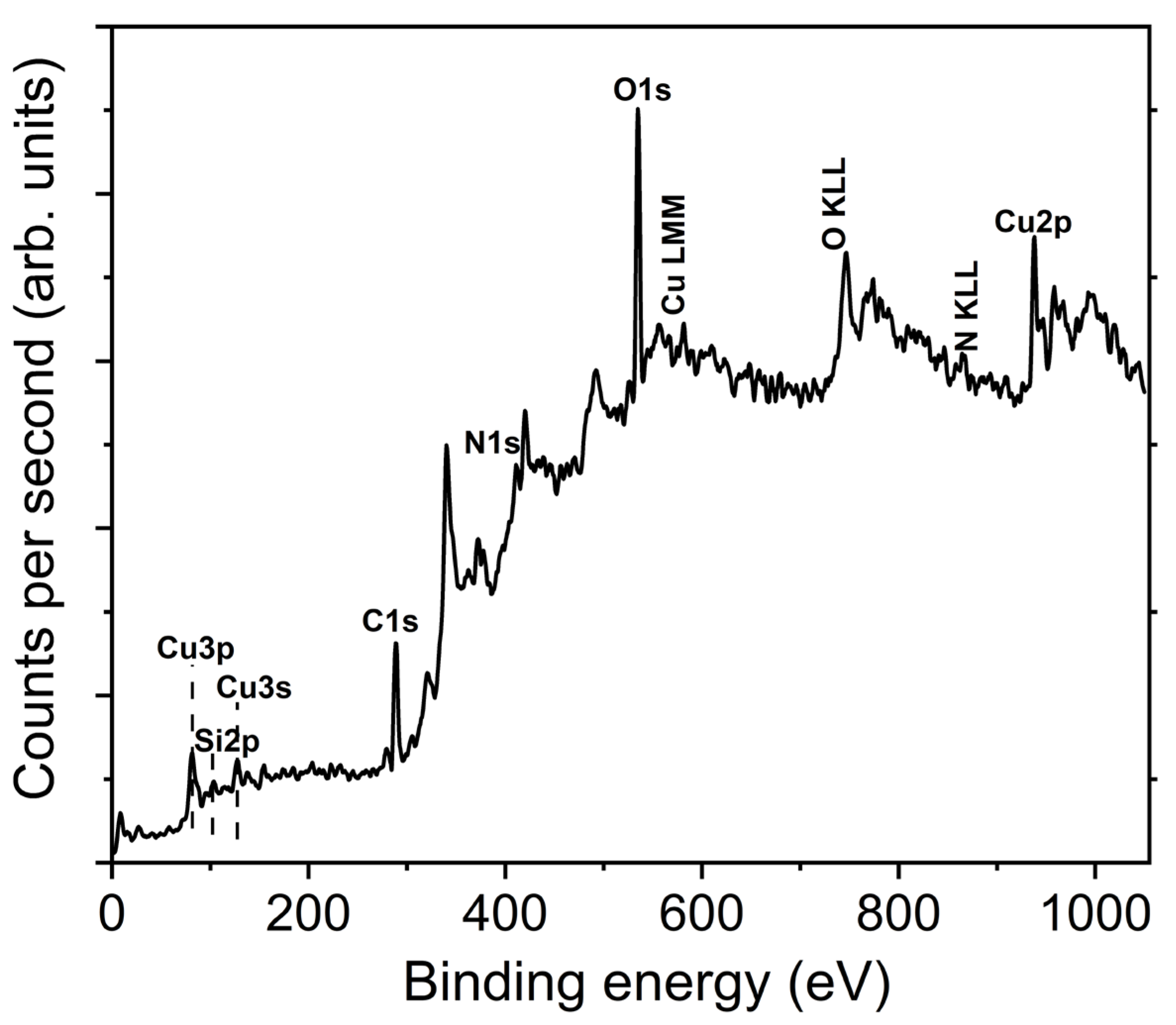
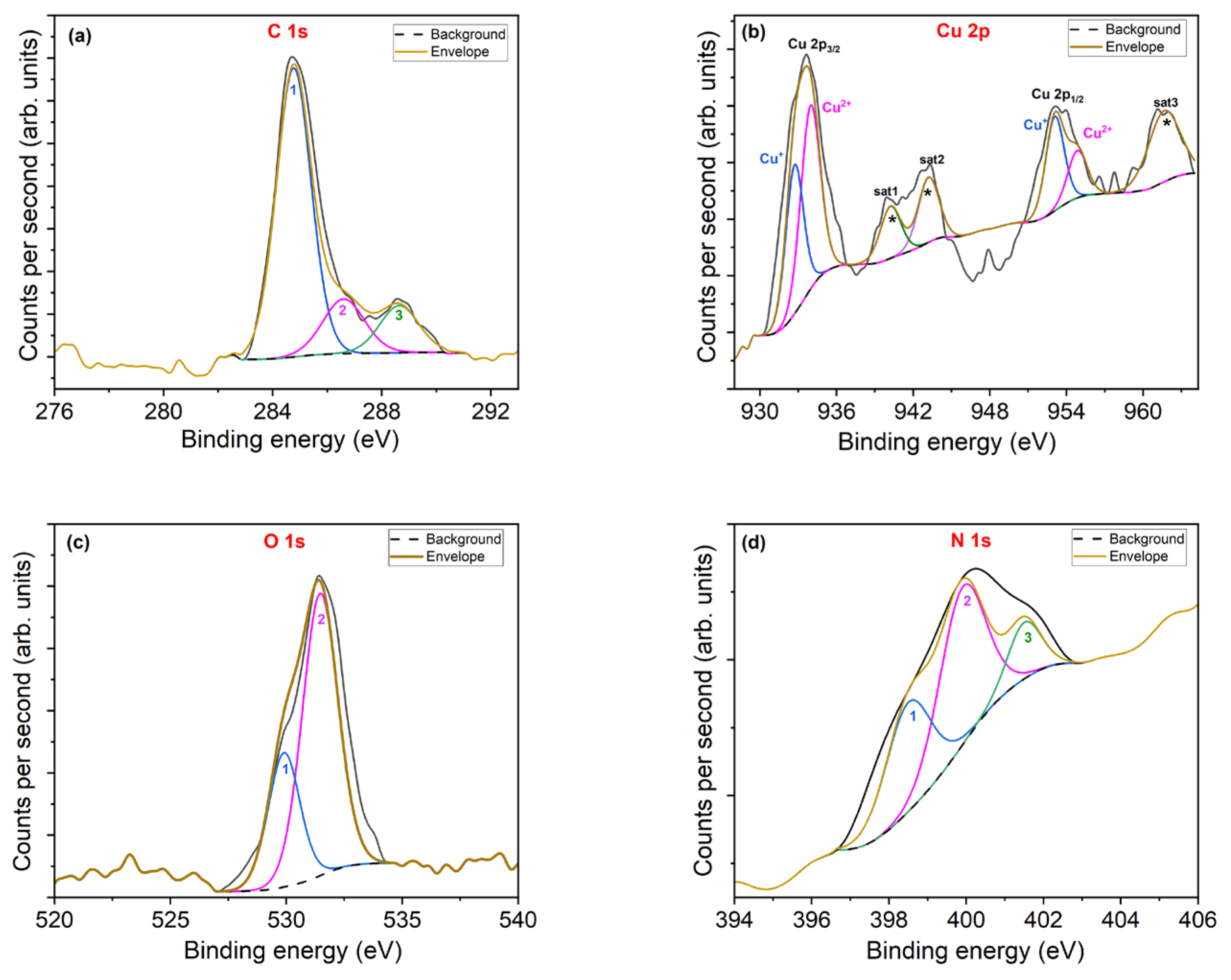
The surface chemistry studied by XPS confirms the presence of copper, nitrogen and oxygen in the samples, and the binding energies of the peaks are attributable to Cu-N and Cu-O bonds.
-
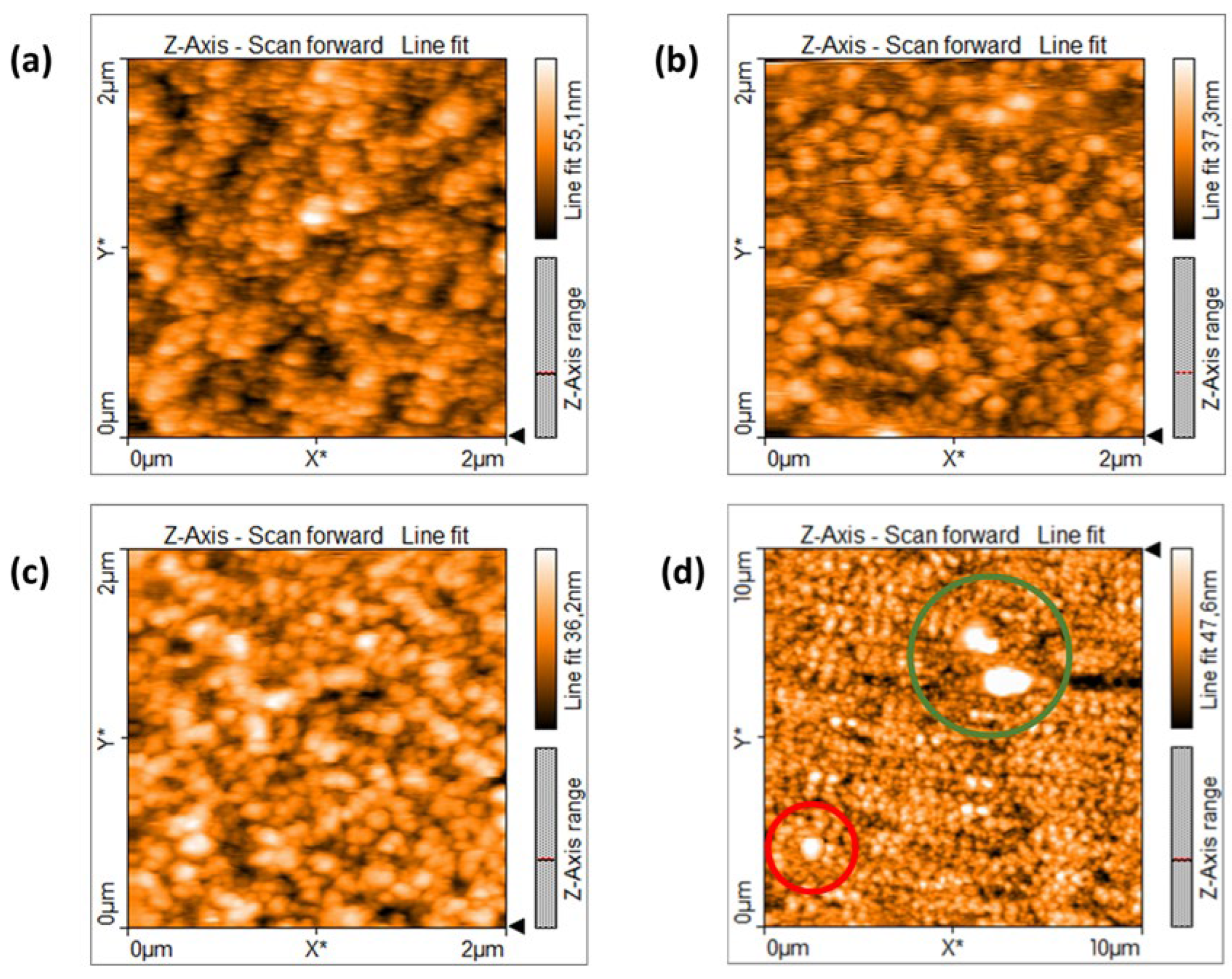
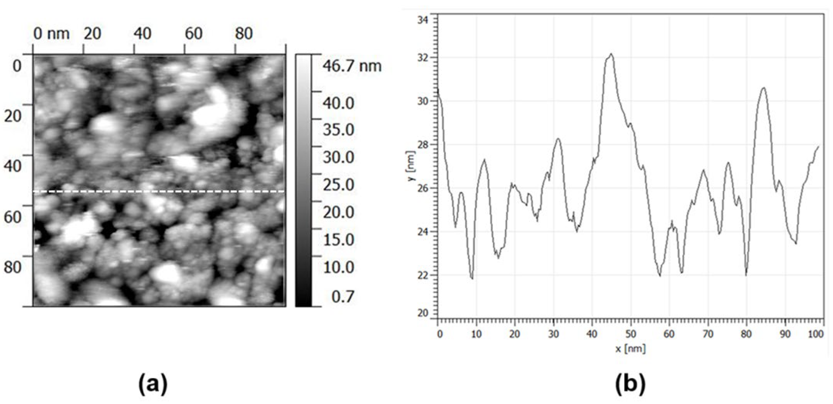
AFM and STM scans show the co-presence of single NP and NP aggregates; NP size is almost the same around 6.6 nm, while aggregates become larger by increasing the spark current.
-
SEM observations confirm AFM morphologies, showing the presence of agglomerates together with NP aggregates with increasing size by increasing Ispark.
Finally, EDS analysis reveals the presence of oxygen in addition to Cu and N, confirming the formation of copper oxides in addition to copper nitride.
From chemical and structural points of view, all the characterization results are in good agreement in confirming the formation of the Cu-N compound together with the Cu-O one. Therefore, it can be affirmed that spark ablation, conducted in N2 atmosphere by using pure metal electrodes, is an effective way to deposit nitride compounds, provided you also accept the formation of oxides. As a matter of fact, the spark generates ionized nitrogen molecules and atoms (N2+ and N+), which participate in the process as active species, able to react with ablated Cu clusters to form nitride compounds. At the same time, nitrogen reacts with the electrodes, too, leading to nitride formation on the Cu electrode that can be ablated as nitride clusters when the spark spot is focused on a nitride region. The same considerations are valid for oxygen, too, which represents, in this case, an undesired presence attributable to contamination coming from the carrier gas bottle [41], in addition to the surface reaction after post-processing exposure to the air ambient. Actually, during our experiments, nitrogen carrier gas is used directly from the tank without any other additional purification system. Therefore, trace impurities of O2 and H2O, together with O and OH radicals and their ions, are generated during the spark in the plasma. In the presence of both oxygen and nitrogen ions, copper immediately reacts with oxygen to form oxide compound, which prevails, although oxygen gas is present in a very small quantity. This is due to the higher electronegativity of oxygen ions compared to nitrogen ones, therefore showing a stronger tendency to bond with metal particles [42]. Even though it has a slower reaction speed, copper reacts with nitrogen ions too, that is the primary gas in the deposition chamber, forming a small fraction of the nitride phase. Thus, these two phases co-exist in the deposited layer. These findings are in good agreement with the literature about the spark ablation of metallic electrodes in N2 atmosphere, where the oxides’ presence is not surprising due to spark deposition being a no-vacuum process [43]. Some strategies have been implemented to obtain unoxidized metal NPs, like sintering [41] or carrier gas mixing with H2 [44,45]. These strategies pave the way to obtain nitride NPs in a close pure form, which strictly requires the minimization of oxygen presence in the chamber to reduce oxide formation, due to the higher reactivity of copper to oxygen ions. The attainment of the nitride phase is not obvious in our experimental conditions, as clearly confirmed in [46] where only Cu and CuO phases were detected by ablating Cu electrodes in N2 atmosphere, with the majority being CuO particles. On the contrary, in a very recent study [47], the authors obtained TiN NPs by the spark ablation of pure Ti electrodes using nitrogen as a carrier gas, also selecting flux rates higher than the one used in this work. This result encourages the study of the role of the nitrogen flow rate to enhance the reaction of nitrogen ions towards copper particles, also keeping in mind that it is a parameter that strongly influences the final average size of NPs and consequently the morphology of the layers. Therefore, accurate optimization will be necessary to achieve the right compromise between the desired NP final size and the nitriding degree.
The morphology results determined by AFM and SEM analyses, where NP aggregates with increasing size following a current increase are observed, can be explained by considering what happens when the spark current is tuned during the ablation process. The current influences the total spark power P supplied by the generator and required to generate the discharge, which is defined as [48] P = I s p a r k · V s p . Ispark is the current that charges the capacitor that periodically releases its energy into the spark, and Vsp is the set-point voltage (1.3 kV) entered by the user (V) that is the mean voltage across that capacitor.
Spark energy E is given by E = 1 2 C V d 2 where C is the capacitance of the capacitor employed in the VS-Particle G1 system (25 nF) and Vd is the discharge voltage that is different to Vsp. Specifically, it is the voltage reached between the two electrodes when the spark happens before dropping to zero when the spark is off, and it depends on the carrier gas and the distance between the electrodes. The relation between Vd and Vsp empirically determined is the following [49]: V d = 1.5 · V s p . Figure 9 clarifies the trend of the voltage between the electrodes over five consecutive sparks taken as an example.
This means that for all the experiments, the discharge voltage is equal to 1.95 kV and the mean spark energy is about 47.5 mJ. The tuning of the current influences the sparking frequency, being equal to f = I C · V d . As a matter of fact, it is equal to 100 Hz, 150 Hz and 200 Hz at 5 mA, 7 mA and 10 mA, respectively. At the same time, the aerosol concentration is affected, too. The Cu NP mass production rate (M) is proportional to spark repetition frequency f and electrode mass ablated per spark ∆m, which increases linearly with the spark energy [50]. It is described by the formula M = f · m . In our experimental conditions, the spark energy is always the same, as previously discussed; therefore, ∆m is constant for all spark currents. The frequency, instead, changes at each deposition process, specifically following the same trend of the current. Therefore, the increase in the spark current leads to higher NP mass production rate M, increasing the probability that the ablated particles collide and agglomerate, generating larger aggregates, as observed by both AFM and SEM analyses.

5. Conclusions

In this work, the spark ablation technique is employed for the deposition of nanoparticles films in a versatile and ambient-friendly way, without resorting to a chemical route, generally requiring solvents and post-processing steps, and producing waste streams. Pure copper electrodes were ablated in nitrogen atmosphere at three different spark currents in order to investigate its effect on the morphology, structure, and chemistry of the samples. The overall result is the co-presence of nanoparticle agglomerates of nitride and oxide due to traces of oxygen in the reactor, as confirmed by XRD, Raman, EDS and XPS analyses, with different sizes according to the spark current, as confirmed by AFM, STM and SEM observations. Copper nitride is known to be a very interesting eco-friendly material for many applications (e.g., ultra-high-capacity cathode material or solar absorber in photovoltaic technology). Moreover, the co-presence of copper oxide and nitride NP aggregates has found increasing interest in the field of antiviral and antibacterial coatings, as it is able to improve these properties. Consequently, the found multi-phase nanostructure coexistence could be exploited for high-performance devices based on the synergy between the properties of a single compound. Future work will be devoted to study the capability to control the nitridation process through the tuning of the carrier gas flow rate to explore (as to exploit, too) the opportunity to obtain a completely nitridated NP layer. In parallel, suitable strategies will be considered to minimize oxide phase formation due to the higher affinity of copper towards oxygen rather than nitrogen.

Author Contributions

Conceptualization, M.A.S., L.N.F., L.V. and A.D.T.; methodology, M.A.S., L.N.F., L.V., A.S., D.M. and A.D.T.; software, L.V.; validation, M.A.S., L.N.F., M.M., R.R., L.V. and A.D.T.; investigation, M.A.S., L.N.F., L.V. and A.D.T.; resources, L.N.F.; data curation, M.A.S., L.N.F., L.V., A.S., D.M. and A.D.T.; writing—original draft preparation, M.A.S., L.N.F., L.V., M.M., A.S. and A.D.T.; supervision, M.A.S., L.N.F., L.V. and A.D.T.; funding acquisition, L.N.F. and R.R. All authors have read and agreed to the published version of the manuscript.

Funding

This research was supported by the “Fit for Medical Robotics” Fit4MedRob Project (Prot PNC0000007, CUP B53C22006900001), funded by the Italian government under the National Plan for Complementary Investments to the National Recovery and Resilience Plan (PNRR), and by the “Platform for CERIC-ERIC Upgrade” PRP@CERIC Project (Prot IR0000028, CUP J97G22000400006) funded by European Union-NextGenerationEU and within the PNRR.

Data Availability Statement

The original contributions presented in this study are included in the article. Further inquiries can be directed to the corresponding author.

Acknowledgments

The authors would like to thank A. Pinna, A. R. Carbone, F. Casino and A. Campa for their valid technical support.

Conflicts of Interest

The authors declare no conflicts of interest.

Abbreviations

The following abbreviations are used in this manuscript:
CuNCopper Nitride
NPsNanoparticles
XRDX-Ray Diffraction
SEMScanning Electron Microscope
STMScanning Tunnelling Microscope
AFMAtomic Force Microscope
RMSRoot Mean Square
UHVUltra-High Vacuum

References

  1. Eker, F.; Duman, H.; Akdaşçi, E.; Bolat, E.; Sarıtaş, S.; Karav, S.; Witkowska, A.M. A Comprehensive Review of Nanoparticles: From Classification to Application and Toxicity. Molecules 2024, 29, 3482. [Google Scholar] [CrossRef] [PubMed]
  2. Srinivasan, L.V.; Rana, S.S. A critical review of various synthesis methods of nanoparticles and their applications in biomedical, regenerative medicine, food packaging, and environment. Discov. Appl. Sci. 2024, 6, 371. [Google Scholar] [CrossRef]
  3. Kohut, A.; Galbacs, G.; Marton, Z.; Geretovszky, Z. Characterization of a copper spark discharge plasma in argon atmosphere used for nanoparticle generation. Plasma Sources Sci. Technol. 2017, 26, 045001. [Google Scholar] [CrossRef]
  4. Siampani, M.; Lazanas, A.C.; Spyrou, K.; Prodromidis, M.I. Eco-friendly spark-generated CoxOy nanoparticle-modifed graphite screen-printed sensing surfaces for the determination of H2O2 in energy drinks. Microchim. Acta 2024, 191, 150. [Google Scholar] [CrossRef]
  5. Mouhtadi, S.; Jurin, F.E.; Buron, C.C.; Pochard, I. Tuning Thin Film Thickness and Porosity with Layer-by-Layer Submicronic Particles Assembly. Chem. Nano Mat. 2024, 10, e202400404. [Google Scholar] [CrossRef]
  6. van Ginkel, H.J.; Vollebregt, S.; Schimd-Ott, A.; Zhang, G.Q. Mass and density determination of porous nanoparticle films using a quartz crystal microbalance. Nanotechnology 2022, 33, 485704. [Google Scholar] [CrossRef]
  7. Available online: https://vsparticle.com/products/research-tools/vsp-p1-nanoprinter (accessed on 20 May 2025).
  8. Majerič, P. Nanostructured materials, structures and mechanical properties, processing and applications. Metall. Mater. Data 2024, 2, 15–22. [Google Scholar] [CrossRef]
  9. Paredes, P.; Rauwel, E.; Rauwel, P. Surveying the Synthesis, Optical Properties and Photocatalytic Activity of Cu3N Nanomaterials. Nanomaterials 2022, 12, 2218. [Google Scholar] [CrossRef]
  10. Chen, Y.H.; Lee, P.I.; Sakalley, S.; Wen, C.K.; Cheng, W.C.; Sun, H.; Chen, S.C. Enhanced Electrical Properties of Copper Nitride Films Deposited via High Power Impulse Magnetron Sputtering. Nanomaterials 2022, 12, 2814. [Google Scholar] [CrossRef]
  11. Yamada, N.; Maruya, K.; Yamaguchi, Y.; Cao, X.; Ninomiya, Y. P- to n-Type Conversion and Nonmetal−Metal Transition of Lithium-Inserted Cu3N Films. Chem. Mater. 2015, 27, 8076–8083. [Google Scholar] [CrossRef]
  12. Rodríguez-Tapiador, M.I.; Merino, J.; Jawhari, T.; Muñoz-Rosas, A.L.; Bertomeu, J.; Fernández, S. Power effect on the properties of copper nitride films as solar absorber deposited in pure nitrogen atmosphere. Appl. Res. 2024, 3, e202200105. [Google Scholar] [CrossRef]
  13. Hussein, H.S. The state of the art of nanomaterials and its applications in energy saving. Bull. Natl. Res. Cent. 2023, 47, 7. [Google Scholar] [CrossRef]
  14. Sahoo, D.; Naik, R. Nanoscience and Nanotechnologies for Photovoltaics. In Handbook of Energy Materials; Gupta, R., Ed.; Springer: Singapore, 2022. [Google Scholar] [CrossRef]
  15. Oni, A.M.; Mohsin, A.S.M.; Rahman, M.M.; Bhuian, M.B.H. A comprehensive evaluation of solar cell technologies, associated loss mechanisms, and efficiency enhancement strategies for photovoltaic cells. Energy Rep. 2024, 11, 3345–3366. [Google Scholar] [CrossRef]
  16. Nakamura, T.; Hiyoshi, N.; Hayashi, H.; Ebina, T. Preparation of plate-like copper nitride nanoparticles from a fatty acid copper(II) salt and detailed observations by high resolution transmission electron microscopy and high-angle annular dark-field scanning transmission electron microscopy. Mater. Lett. 2015, 139, 271–274. [Google Scholar] [CrossRef]
  17. Feng, J.; Biskos, G.; Schmidt-Ott, A. Toward industrial scale synthesis of ultrapure singlet nanoparticles with controllable sizes in a continuous gas-phase process. Sci. Rep. 2015, 5, 15788. [Google Scholar] [CrossRef]
  18. Figueira, C.A.; Rosario, G.D.; Pugliese, D.; Rodríguez-Tapiador, M.I.; Fernández, S. Effect of Argon on the Properties of Copper Nitride Fabricated by Magnetron Sputtering for the Next Generation of Solar Absorbers. Materials 2022, 15, 8973. [Google Scholar] [CrossRef]
  19. Trivedi, A.; Thakarda, J.; Chavda, N.; Agrawal, Y.K.; Maity, P. A new route towards selective synthesis of supported Cu2O and CuO nanoparticles under extremely mild condition. Nano-Struct. Nano-Objects 2016, 6, 34–38. [Google Scholar] [CrossRef]
  20. Devaraj, P.; Peranantham, P.; Jeyachandran, Y.L. Oxidation behavior of copper nitride thin films deposited by direct current magnetron sputtering. J. Mater. Sci. Mater. Electron. 2021, 32, 27899–27912. [Google Scholar] [CrossRef]
  21. Arulkumar, E.; Thanikaikarasan, S.; Tesfie, N. Influence of Deposition Parameters for Cu2O and CuO Thin Films by Electrodeposition Technique: A Short Review. J. Nanomater. 2023, 2023, 8987633. [Google Scholar] [CrossRef]
  22. Rodríguez-Tapiador, M.I.; Asensi, J.M.; Roldán, M.; Merino, J.; Bertomeu, J.; Fernández, S. Copper Nitride: A Versatile Semiconductor with Great Potential for Next-Generation Photovoltaics. Coatings 2023, 13, 1094. [Google Scholar] [CrossRef]
  23. Rodríguez-Tapiador, M.I.; Merino, J.; Jawhari, T.; Muñoz-Rosas, A.L.; Bertomeu, J.; Fernández, S. Impact of the RF Power on the Copper Nitride Films Deposited in a Pure Nitrogen Environment for Applications as Eco-Friendly Solar Absorber. Materials 2023, 16, 1508. [Google Scholar] [CrossRef] [PubMed]
  24. Sajeev, A.; Paul, A.M.; Nivetha, R.; Gothandapani, K.; Gopal, T.S.; Jacob, G.; Muthuramamoorty, M.; Pandiaraj, S.; Alodhayb, A.; Kim, S.Y.; et al. Development of Cu3N electrocatalyst for hydrogen evolution reaction in alkaline medium. Sci. Rep. 2022, 12, 2004. [Google Scholar] [CrossRef] [PubMed]
  25. Lee, W.-J.; Chang, Y.-H. Growth without Post-annealing of Monoclinic VO2 Thin Film by Atomic Layer Deposition Using VCl4 as Precursor. Coatings 2018, 8, 431. [Google Scholar] [CrossRef]
  26. Mahendra, G.; Malathi, R.; Kedhareswara, S.P.; Lakshmi-Narayana, A.; Dhananjaya, M.; Guruprakash, N.; Hussain, O.M.; Mauger, A.; Julien, C.M. RF Sputter-Deposited Nanostructured CuO Films for Micro-Supercapacitors. Appl. Nano 2021, 2, 46–66. [Google Scholar] [CrossRef]
  27. Chen, S.; Brown, L.; Levendorf, M.; Cai, W.; Ju, S.Y.; Edgeworth, J.; Li, X.; Magnuson, C.W.; Velamakanni, A.; Piner, R.D.; et al. Oxidation resistance of graphene-coated Cu and Cu/Ni alloy. ACS Nano 2011, 5, 1321–1327. [Google Scholar] [CrossRef]
  28. Olszok, V.; Bierwirth, M.; Weber, A.P. Interaction of Reactive Gases with Platinum Aerosol Particles at Room Temperature: Effects on Morphology and Surface Properties. Nanomaterials 2021, 11, 2266. [Google Scholar] [CrossRef]
  29. Beverina, M.; Sanchez-Cortes, S.; Schabes, F.I.; Zapata, J.; Arias Cassara, M.L.; Tuttolomondo, M.E. Spectroscopic characterization (Raman and infrared) of Aloe maculata from the north Argentina region. Vib. Spectrosc. 2022, 122, 103423. [Google Scholar] [CrossRef]
  30. Biesinger, M.C.; Lau, L.W.M.; Gerson, A.R.; Smart, R.S.C. Resolving surface chemical states in XPS analysis of first row transition metals, oxides and hydroxides: Sc, Ti, V, Cu and Zn. Appl. Surf. Sci. 2010, 257, 887–898. [Google Scholar] [CrossRef]
  31. Biesinger, M.C. Advanced analysis of copper X-ray photoelectron spectra. Surf. Interface Anal. 2017, 49, 1325–1334. [Google Scholar] [CrossRef]
  32. Gallardo-Vega, C.; De la Cruz, W. Study of the structure and electrical properties of the copper nitride thin films deposited by pulsed laser deposition. App. Surf. Sci. 2006, 252, 8001–8004. [Google Scholar] [CrossRef]
  33. Jiang, J.; Liu, X.X.; Han, J.; Hu, K.; Chen, J.S. Self-Supported Sheets-on-Wire CuO@Ni(OH)2/Zn(OH)2 Nanoarrays for High-Performance Flexible Quasi-Solid-State Supercapacitor. Processes 2021, 9, 680. [Google Scholar] [CrossRef]
  34. Sithole, R.K.; Machogo-Phao, L.F.E.; Kolokoto, T.; Zimuwandeyi, M.; Gqoba, S.S.; Mubiayi, K.P.; Moloto, M.J.; Van Wyk, J.; Moloto, N. Elucidating the effect of precursor decomposition time on the structural and optical properties of copper(i) nitride nanocubes. RSC Adv. 2020, 10, 34231–34246. [Google Scholar] [CrossRef] [PubMed]
  35. Morales, J.; Sanchez, L.; Martin, F.; Ramos-Barrado, J.R.; Sanchez, M. Use of low-temperature nanostructured CuO thin films deposited by spray-pyrolysis in lithium cells. Thin Solid Films 2005, 474, 133–140. [Google Scholar] [CrossRef]
  36. Guerrero-Araque, D.; Acevedo-Peña, P.; Ramírez-Ortega, D.; Lartundo-Rojas, L.; Gómez, R. SnO2–TiO2 structures and the effect of CuO, CoO metal oxide on photocatalytic hydrogen production. J. Chem. Technol. Biotechnol. 2017, 92, 1531–1539. [Google Scholar] [CrossRef]
  37. Miura, A.; Takei, T.; Kumada, N. Synthesis of Cu3N from CuO and NaNH2. J. Asian Ceram. Soc. 2014, 2, 326–328. [Google Scholar] [CrossRef]
  38. Fan, X.; Wu, Z.; Li, H.; Geng, B.; Li, C.; Yan, P. Morphology and thermal stability of Ti-doped copper nitride films. J. Phys. D Appl. Phys. 2007, 40, 3430–3435. [Google Scholar] [CrossRef]
  39. Chen, X.; Burda, C. Photoelectron Spectroscopic Investigation of Nitrogen-Doped Titania Nanoparticles. J. Phys. Chem. B 2004, 108, 15446–15449. [Google Scholar] [CrossRef]
  40. Aghajani, S.; Accardo, A.; Tichem, M. Aerosol Direct Writing and Thermal Tuning of Copper Nanoparticle Patterns as Surface-Enhanced Raman Scattering Sensors. ACS Appl. Nano Mater. 2020, 3, 5665–5675. [Google Scholar] [CrossRef]
  41. Ternero, P.; Sedrpooshan, M.; Wahlqvist, D.; Meuller, B.O.; Ek, M.; Hubner, J.-M.; Westerstrom, R.; Messing, M.E. Effect of the carrier gas on the structure and composition of Co–Ni bimetallic nanoparticles generated by spark ablation. J. Aerosol Sci. 2023, 170, 106146. [Google Scholar] [CrossRef]
  42. Maisser, A.; Barmpounis, K.; Holm, S.; Attoui, M.; Schmidt-Ott, A.; Kangasluoma, J.; Biskos, G. Characterization of atmospheric-pressure spark generated atomic silver and gold clusters by time-of-flight mass spectrometry. J. Aerosol Sci. 2021, 156, 105780. [Google Scholar] [CrossRef]
  43. Hagen, F.P.; Rinkenburger, A.; Günther, J.; Bockhorn, H.; Niessner, R.; Suntz, R.; Loukou, A.; Trimis, D.; Haisch, C. Spark discharge-generated soot: Varying nanostructure and reactivity against oxidation with molecular oxygen by synthesis conditions. J. Aerosol Sci. 2020, 143, 105530. [Google Scholar] [CrossRef]
  44. Preger, C.; Bulbucan, C.; Meuller, B.O.; Ludvigsson, L.; Kostanyan, A.; Muntwiler, M.; Deppert, K.; Westerstrom, R.; Messing, M.E. Controlled oxidation and self-passivation of bimetallic Magnetic FeCr and FeMn aerosol nanoparticles. J. Phys. Chem. C 2019, 123, 16083–16090. [Google Scholar] [CrossRef]
  45. Kohut, A. Hydrogen-assisted spark generation of silver nanoparticles: The effect of hydrogen content on the signal intensity in surface-enhanced Raman spectroscopy. J. Aerosol Sci. 2023, 167, 106090. [Google Scholar] [CrossRef]
  46. Giannakopoulos, K.; Lasithiotakis, M.; Karakasis, C.; Gini, M.; Gardelis, S.; Karakasiliotis, I.; Mouti, N.; Xesfyngi, Y.; Manolis, G.K.; Georgoutsou-Spyridonos, M.; et al. Spark Discharge Aerosol-Generated Copper-Based Nanoparticles: Structural & Optical Properties; Application on the Antiviral (SARS-CoV-2) and Antibacterial Improvement of Face Masks. ChemPlusChem 2024, 89, e202400194. [Google Scholar] [CrossRef]
  47. Radovanović-Perić, F.; Burtscher, M.; Panžić, I.; Kiener, D.; Mandić, V. Novel ambient-condition solid-state synthesis route of nanocrystalline TiN thin films via spark plasma ablation deposition. Ceram. Int. 2025, 51, 5576–5582. [Google Scholar] [CrossRef]
  48. Loizidis, C.; Petallidou, K.C.; Maisser, A.; Bezantakos, S.; Pfeiffer, T.V.; Schmidt-Ott, A.; Biskos, G. Insights into the enhancement of nanoparticle production throughput by atmospheric-pressure spark ablation. Aerosol Sci. Technol. 2024, 58, 1421–1431. [Google Scholar] [CrossRef]
  49. Petallidou, K.C.; Schmidt-Ott, A.; Biskos, G. Stability of nanoparticle production by atmospheric-pressure spark ablation. Aerosol Sci. Technol. 2024, 58, 1079–1088. [Google Scholar] [CrossRef]
  50. Feng, J.; Guo, X.; Ramlawi, N.; Pfeiffer, T.V.; Geutjens, R.; Basak, S.; Nirschl, H.; Biskos, G.; Zandbergen, H.W.; Schmidt-Ott, A. Green manufacturing of metallic nanoparticles: A facile and universal approach to scaling up. J. Mater. Chem. A 2016, 4, 11222–11227. [Google Scholar] [CrossRef]
Figure 1. (a) Schematic of spark ablation system used for depositions; (b) classical circuit of spark nanoparticle generator; (c) photograph of system used in this work.
Crystals 15 00587 g001
Figure 2. XRD patterns of the samples deposited at different Ispark.
Crystals 15 00587 g002
Figure 3. Raman spectroscopy spectra of copper nitride nanostructured aggregates.
Crystals 15 00587 g003
Figure 4. Large-area survey spectrum for representative as-received sample (10 mA).
Crystals 15 00587 g004
Figure 5. The high-resolution XPS spectra of the (a) C 1s, (b) Cu-2p, (c) O 1s, (d) N 1s core peaks fit into sub-peaks. In the panel (b) the satellite peaks are indicated by asterisks.
Crystals 15 00587 g005
Figure 6. AFM images of copper NPs by tuning the spark current during the growth process in N2 atmosphere; (a) Ispark = 5 mA, (b) Ispark = 7 mA, (c) Ispark = 10 mA, (d) spheres (red circle) and agglomerates (green circle) randomly distributed on the surface of the sample ablated at a current of 10 mA taken as representative.
Crystals 15 00587 g006
Figure 7. (a) STM topographical image of one representative sample (10 mA) of spark-ablated Cu NPs (scans at 1 V, 60 pA); (b) line profile representations of NPs.
Crystals 15 00587 g007
Figure 8. SEM images of the samples ablated at 5 mA (a), 7 mA (b) and 10 mA (c). EDS images of the sample ablated at 10 mA (c).
Crystals 15 00587 g008
Figure 9. Voltage trend during spark ablation process over five consecutive sparks.
Crystals 15 00587 g009
Table 1. Deposition parameters set during the experiments.
Parameters Values
Vsp1.3 kV
N2 flux5 L/min
Deposition time300 s
Ispark (tuned)5-7-10 mA
Espark47.5 mJ
Table 2. Summary of XPS data obtained from fitting calculations regarding binding energy values, full width at half maximum (FWHM), area and percentage of each fitting component.
BE (eV)FWHMAREA%AREA
C1s
1284.81.5220270.8
2286.61.849916
3288.61.740613.1
Cu2p3/2
Cu+932.81.6223418.8
Cu2+933.91.8316525
sat1940.21.99597.8
sat2943.21.911919.8
Cu2p1/2
Cu+953.11.7153612.9
Cu2+954.91.88146.9
sat3961.83209518
O1s
1529.91.8445770.2
2531.51.6189429.8
N1s
1398.71.424135.1
24001.435351.4
3401.619213.4
Disclaimer/Publisher’s Note: The statements, opinions and data contained in all publications are solely those of the individual author(s) and contributor(s) and not of MDPI and/or the editor(s). MDPI and/or the editor(s) disclaim responsibility for any injury to people or property resulting from any ideas, methods, instructions or products referred to in the content.

