Article

Epitaxial Growth of BaBiO3 Thin Films on SrTiO3(001) and MgO(001) Substrates Using Molecular Beam Epitaxy: Controlling the Competition Between Crystal Orientations

1
IMEC, Kapeldreef 75, 3001 Leuven, Belgium
2
Department of Materials Engineering, KU Leuven, Kasteelpark Arenberg 44, 3001 Leuven, Belgium
3
Department of Chemistry, KU Leuven, Celestijnenlaan 200F, 3001 Leuven, Belgium
*
Author to whom correspondence should be addressed.
Crystals 2025, 15(6), 534; https://doi.org/10.3390/cryst15060534
Submission received: 16 April 2025 / Revised: 28 May 2025 / Accepted: 1 June 2025 / Published: 2 June 2025

Abstract

:
BaBiO3 has recently gained significant research attention as a parent material for an interesting family of alloyed compositions with multiple technological applications. In order to grow a variety of structures, a versatile deposition tool such as molecular beam epitaxy must be employed. In this work, the molecular beam epitaxy growth of BaBiO3 on SrTiO3(001) and MgO(001) substrates is studied. When grown by molecular beam epitaxy on SrTiO3(001) or MgO(001) substrates, BaBiO3 is known to have two competing orientations, namely (001) and (011). Characterization of the thin film is carried out by X-ray diffraction, X-ray reflectivity, atomic force microscopy, Rutherford backscattering, and transmission electron microscopy. Pathways to block the growth of BaBiO3(011) and to grow only the technologically relevant BaBiO3(001) are described for both substrates. An understanding of the enabling mechanism of the co-growth is established from an epitaxial point of view. This can be beneficially utilized for the growth of different compositions in the BaBiO3 material family in a more controlled manner.

1. Introduction

Thanks to their chemical and structural versatility, complex oxides have attracted significant research interest over the past few decades [1,2]. Perovskite oxide is a family of compounds that belongs to the class of complex oxides and has an ABO3 crystal structure [3]. BaBiO3 (BBO) is a perovskite compound that was first synthesized in 1963 [4]. BBO has a monoclinic structure at room temperature and a cubic structure at temperatures above 820 K [5]. In contrast with the band theory of solids, BBO has a band gap of 2–2.19 eV [6,7]. Thanks to its electronic properties, BBO has been investigated for a wide range of technological applications, like efficient photocatalytic harvesters [8], photovoltaic devices [9], water splitting [10], and CO2 degradation [11]. BBO shows ferroelectric behavior when grown on a Pt-coated Si substrate [12], while BBO nanoparticles exhibit a ferromagnetic response [13], making the material promising for memory applications. BBO may also serve as a favorable buffer layer for other perovskite oxide thin films with large lattice constants, such as YBiO3 (a = 4.4 Å) [14].
Besides self-doping, alloying could potentially widen the application area of a certain parent material by strongly tailoring its electronic, optical, or structural properties [15]. Perovskite oxides serve as versatile parent compounds thanks to the possible substitution on any of the three different ionic sites that exist within the ABO3 structure. When applied to our parent material of interest, BBO, many examples can be found in the literature. One example is the discovery of superconductivity for n-type doped BaBi1−xPbxO3, with a critical temperature of 13 K [16]. Ba1−xKxBiO3 and Ba1−xRbxBiO3 (p-type doped BBO) were later discovered as superconductor oxides with a transition temperature of 29.8 K [17]. Partial n-type anionic substitution led to the discovery of topological insulating BaBi(O1−xFx)3 in a density functional theory (DFT) study [18]. If experimentally realized, BaBi(O1−xFx)3 could feasibly be implemented in technologies such as magnetics, thermoelectrics, or quantum computing [19,20,21]. Visibly transparent p-type semiconducting layers based on Ba1−xKxBi1−xTaxO3, with a maximum hole mobility of around 30 cm2/V.s and an increased band gap of 4.5 eV [22], have been discovered. Alongside its counterpart, n-type transparent In-Ga-Zn-O (with an electron mobility higher than 100 cm2/V.s) [23], this material system is very important for enabling complementary metal–oxide–semiconductor (CMOS)-based thin-film transistor technology. Molecular beam epitaxy (MBE) has the ability to grow an alloyed thin film with a variety of compositions in a controlled manner [24].
Understanding the growth mechanism, phase stability, and kinetics of the parent perovskite thin film is an essential prerequisite for developing high-quality alloyed structures. Based on its co-deposition capability in ultra-high-vacuum environments, MBE is considered advantageous in controlling the stoichiometry and crystal orientation (important aspects for realizing the desired technological edge) of the grown thin film [24]. Accessing a growth window where the cations’ stoichiometry is self-regulating has been made possible by MBE thanks to the presence of a volatile elemental component [25]. In our previous study, the epitaxy of BBO was shown to follow an adsorption-controlled regime when grown on SrTiO3(STO)-buffered Si(001) substrates [26]. Alongside the MBE parameters, which play a crucial role in epitaxy, substrate choice is also very important, as it influences the crystal orientation and film quality. BBO(001) and BBO(011) are known to be competing orientations in thin-film growth according to previous studies [26,27,28,29,30,31], depending on the substrate of choice. In this study, the MBE growth of BBO thin films on both STO ( a STO = 3.905 Å) and MgO ( a MgO = 4.212 Å) substrates is investigated. The crystal quality and phase formation of the various BBO thin films, grown using different growth parameters, are assessed. The influence of using a BaO buffer layer on the crystal orientation and morphology of the thin film grown on the STO substrate is also demonstrated.

2. Materials and Methods
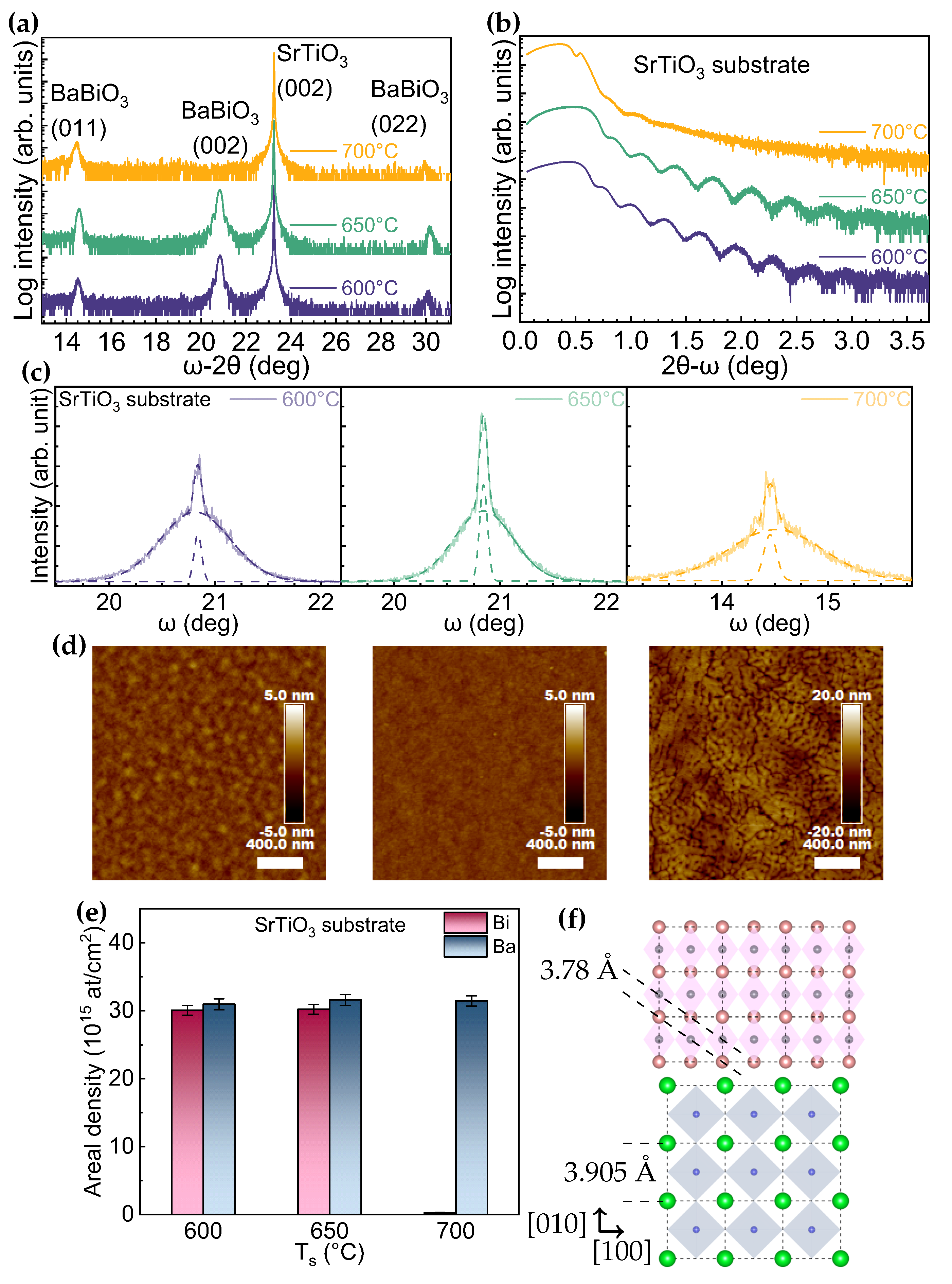
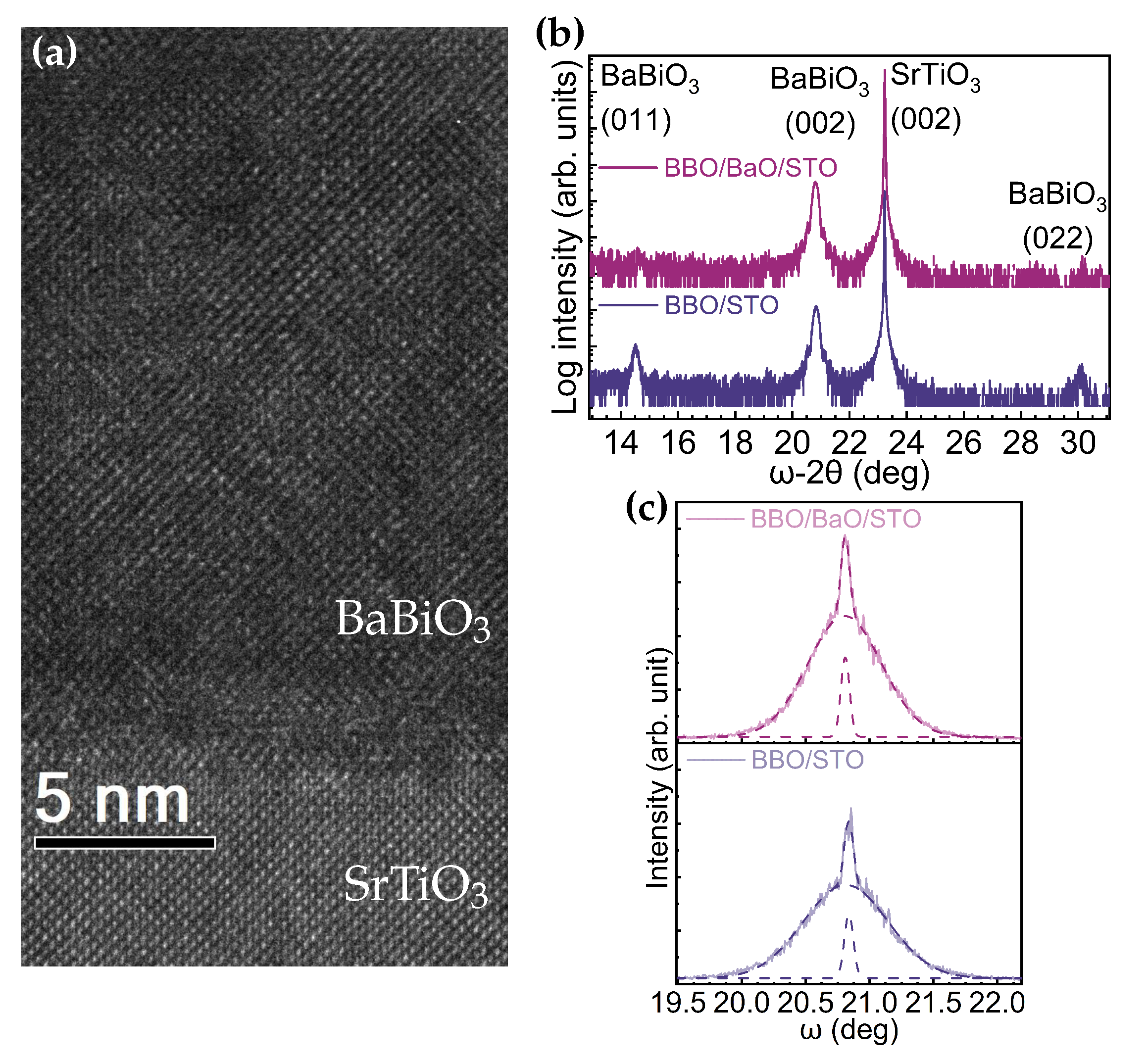
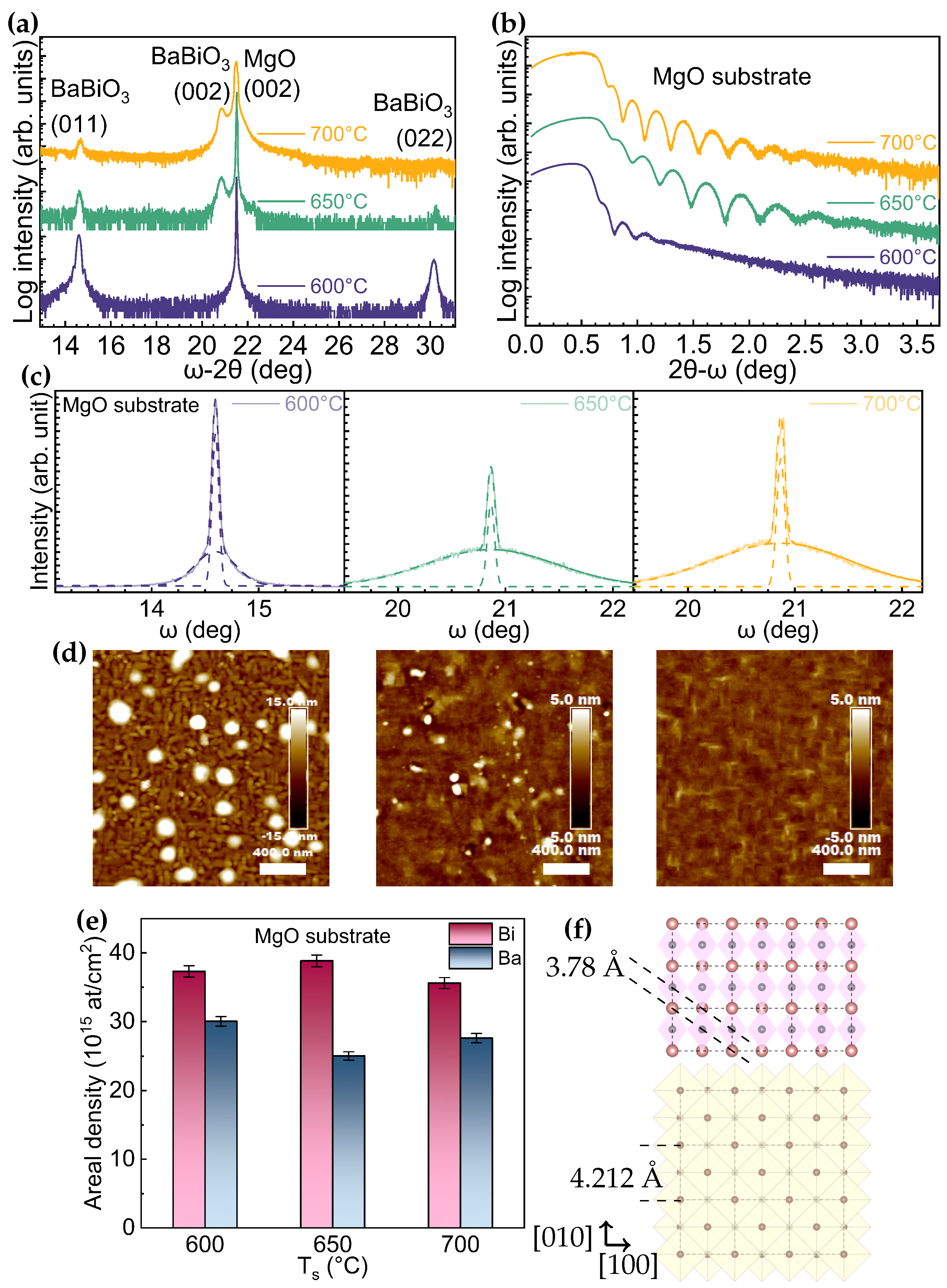
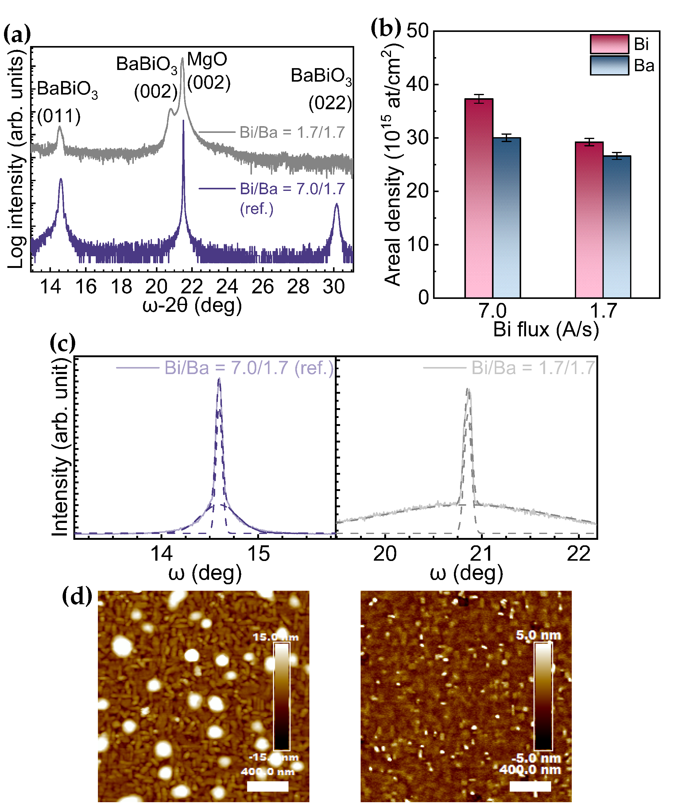
To understand the growth mechanism for BBO thin films on both STO and MgO bulk substrates (Furuuchi Chemical Co., Tokyo, Japan), an ultra-high-vacuum MBE reactor was utilized. Bulk substrates measuring 10 mm × 10 mm were cleaned before introduction into the tool by dipping them into isopropanol for a few hours, followed by an overnight acetone bath. The substrate coupons were then glued onto a carrier wafer. Before MBE’s growth started, the surface of the glued coupons was further cleaned by heat treatment in an oxygen environment at 800 °C for 30 min. Metallic sources were evaporated out of their thermal effusion cells toward the rotating substrates after calibrating the fluxes using an in situ quartz crystal microbalance (QCM) setup. Growth was carried out in an activated oxygen species environment, generated using a remote radio-frequency (RF) plasma cell, with a background pressure of 3E-6 Torr and a plasma power of 600 W. The thin films were cooled down from growth temperature (Ts) to room temperature at a rate of approximately 10 °C/min under the same oxygen conditions.
The crystalline structure and quality of the thin films were checked utilizing an X-ray diffraction (XRD) setup with Cu-Kα radiation. Symmetric ω –2 θ scans were collected at scattering angles between 13° and 31° for all samples, with a step size of 0.006°, alongside the rocking curves (RCs) around the relevant diffraction peaks. Using the same setup, the thickness and roughness of the thin films were deduced based on X-ray reflection (XRR) measurements. A transmission electron microscopy (TEM) technique with a 200 kV operating voltage was used to further evaluate the crystal structure of one of the thin films. Sample preparation for TEM inspection was minimized to avoid any damage to the e-beam-sensitive BBO layer. Surface morphology investigation was carried out with an atomic force microscope (AFM) operating in tapping mode. AFM images of 512 scan lines were collected under ambient conditions by a cantilever with an amplitude of oscillation of 75 nm and a scanning rate of 0.5 Hz. To overcome external sources of noise, the AFM setup was enclosed in its cabinet during measurements, and the setup was placed on a vibration-isolation table in a temperature-stable lab environment. The NSC19 cantilever (MikroMasch©, Sofia, Bulgaria) used in this study has a stiffness of 3.5 N/m and a tip radius of 8 nm. Regarding height calibration, a Bruker© Si calibration standard (VGRP-UM) with a depth of 180 nm was used. The evaluation of the elemental composition of the grown thin films was performed using the Rutherford backscattering (RBS) method.

3. Results

In Figure 1, the variation in Ts is shown for the thin films grown at 600 °C, 650 °C, and 700 °C on the STO substrate. The metallic fluxes were kept at JBi = 7 A/s and JBa = 1.7 A/s. According to the symmetric out-of-plane XRD scans in Figure 1a, diffraction peaks can be observed at roughly 20.8° and 14.5° for the thin films grown at 600 °C and 650 °C. This demonstrates that the co-growth of BBO(001) and BBO(011) took place. At 700 °C, only one diffraction peak can be observed at 14.54°. The crystalline quality can be evaluated based on the RC scans in Figure 1c, which show a broad peak corresponding to the interfacial area with high defect and dislocation densities in addition to a sharp peak indicating highly ordered epitaxial areas in the films [32]. At 600 °C and 650 °C, the sharp peaks have a full width at half maximum (FWHM) of 0.084° and 0.088°, respectively, indicating high-quality epitaxy at these temperatures. The XRR data in Figure 1b for the thin films grown at 600 °C and 650 °C show that the surface and interface roughnesses are low, with clearly distinguishable Kiessig fringes and thicknesses of 30 nm and 27 nm, respectively. On the other hand, the thin film grown at 700 °C has higher roughness and a thickness of 35 nm, extracted with lower accuracy due to the roughness-induced oscillation rapid damping [33]. The AFM surface texture of the film grown at 700 °C is visibly different in comparison with the other two films, with root mean square (RMS) roughness of 3.5 nm, while at lower temperatures, it is below 0.4 nm, as illustrated in Figure 1d. The RBS data in Figure 1e show that the films grown at 600 °C and 650 °C are nearly stoichiometric (Bi/Ba = 0.97 and 0.96, respectively); however, almost no Bi incorporation occurs at 700 °C.
One of the most common approaches used to stabilize a certain orientation in epitaxy is the use of a buffer layer [34,35]. According to Figure 2b, it is clear that growing a BaO buffer layer helps stabilize only the (001) phase of BBO, with only one diffraction peak at ω BBO = 20.81°. The thin film with a BaO buffer layer has an RC FWHM of 0.079°, in accordance with its sharp peak in Figure 2c, denoting high crystalline quality. The growth of BBO(001) can also be observed in the TEM image in Figure 2a with the aid of a BaO buffer layer. The reason a monolayer of BaO as a buffer layer helps stabilize only the BBO(001) orientation is discussed in Section 4.
For the MgO substrate, as shown in Figure 3a, diffraction peaks at 14.6°, with varying intensities, can be observed at all temperatures, but 20.85° only at 650 °C and 700 °C. The FWHMs of the sharp peaks of the RC scans are 0.076°, 0.081°, and 0.087° at 600 °C, 650 °C, and 700 °C, respectively. The high roughness of the layer grown at 600 °C is evident based on the XRR data in Figure 3b. Diffuse scattering results in the damping of the reflected radiation intensity due to incoherent interference. Unlike the smooth layers grown on the STO substrate, the XRR oscillations of the thin films grown on MgO at 650 °C and 700 °C do not have a fixed fringe width; therefore, the calculated thicknesses are 32 ± 3 nm and 38 ± 5 nm, respectively. According to the AFM data in Figure 3d, the surface of thin films grown on the MgO substrate becomes smoother as the temperature increases, with RMS roughness of 4.5 nm at 600 °C, 0.9 nm at 650 °C, and 0.5 nm at 700 °C. Islands with an average diameter of 90 nm and a height of 27 nm, observed for the thin films grown at 600 °C, are the root cause of this high roughness. The RBS data in Figure 3e indicate that all layers are Bi-rich: Bi/Ba = 1.24, 1.55, and 1.29 at 600 °C, 650 °C, and 700 °C, respectively.
Upon decreasing the flux ratio from JBi/JBa = 7.0/1.7 to JBi/JBa = 1.7/1.7, a notable reduction in the diffraction peak at 14.57° and the appearance of another one at 20.81° can be seen in the out-of-plane XRD results in Figure 4a. This is associated with a more stoichiometric layer, as indicated by the RBS data in Figure 4b, showing a Bi/Ba ratio of 1.09 (15% reduction in the film’s Bi content). At JBi = 1.7 Å/s, BBO(001) can be grown with a sharp-peak FWHM of 0.088°, as indicated by the RC data in Figure 4c. In addition, as shown in Figure 4d, the surface appears to be smoother, with an RMS roughness of 1 nm and no visible large islands. The reported observations are summarized in Table 1.

4. Discussion

According to the XRD data, either the growth of BBO(011) or the co-growth of BBO(011) and BBO(001) can be observed when growing the material on either an STO or MgO substrate. BBO(011) has previously been reported as the preferred orientation, either solely or in combination with BBO(001), when grown on an STO(001) substrate by MBE [28]. This contradicts its growth by pulsed laser deposition (PLD), where BBO(001) was obtained on STO(001), with a spontaneously occurring structurally different reconstruction layer of almost 1 nm at the interface [14,37,38]. BBO(011) has also previously been obtained on an MgO(001) substrate, despite a low lattice mismatch [27] of around 3%, compared to 11% on STO. This raises the question of how two in-plane domain orientations coexist in a similar way for the two different substrates. It is unexpected to obtain the (011) orientation on either STO(001) or MgO(001) (both with non-polar surfaces), especially since the BBO(011) orientation is polar. Additionally, the surface energies of (011) orientations are typically higher than those of (001) orientations for most perovskite compounds, as shown by DFT studies, regardless of their terminations [39,40]. Therefore, under certain thermodynamic conditions, the same orientation epitaxy is expected for the growth of bismuthate.
However, to explain the growth of BBO(011) on an STO substrate, the problem has to be considered from an epitaxial point of view. At the interface, this orientation seems to have a favorable relationship with the substrate BBO(011) [110]‖STO(001) [100]. This way, half of BBO(011)’s unit cell diagonal, with a lattice spacing of 3.78 Å, aligns commensurately with one unit cell of STO, lowering the lattice mismatch to only −3%. According to the AFM results, this orientation is as smooth as that of BBO(001), unlike when it is grown on an MgO substrate. This is due to the fact that, with a large lattice mismatch of −11% for BBO(011)[110]‖MgO(001)[100], high strain energy drives the system to randomly form 3D islands. A temperature of 650 °C does not appear to provide enough energy for the adatoms to find their lowest energy sites, which, intuitively, occurs when BBO(001) is primarily formed at a higher temperature of 700 °C, resulting in a much smoother surface. It can be deduced that the presence of the BBO(011) orientation in thin films grown on an MgO substrate is associated with island growth and high surface roughness, as shown in the Supplementary Materials. Atomic schematics showing the lattice plane BBO(011) are presented relative to the STO and MgO substrates in Figure 1f and Figure 2f, respectively. Such orientation competition has been observed multiple times in the literature for oxide materials, such as STO on CeO2 [41], Ba0.8Sr0.2TiO3 on LaAlO3 [42], and MgO on ZnO [43].
BBO(001) was previously grown on an STO(001) substrate using PLD. A naturally occurring wetting layer at the interface has been reported [14,37,38], which is believed to uncouple the layer from the substrate through dislocation formation and to enable domain-matching epitaxy. A detailed TEM study showed that this reconstructed layer consists of a double layer in the form of δ -Bi2O3 with a fluorite structure and an orientation of STO (001)[100]‖ δ -Bi2O3(001)[110]‖BBO (001)[100] [38]. A BaO buffer layer with an in-plane lattice spacing of 5.53 Å was grown in registry with STO, exhibiting an epitaxial relationship of BaO[100]‖STO[110], where a STO 2 = 5.52 Å. From an epitaxial point of view, this facilitates the formation of the fluorite δ -Bi 2O 3 with a lattice constant of α-Bi2O3 = 5.65 Å [38], which ultimately enables the single-orientation growth of BBO(001) on an STO(001) substrate.
The thin films grown on the STO substrate at 700 °C have no bismuth incorporated due to the low elemental sticking coefficient as the temperature increases. However, the observation of a diffraction peak at 14.54° denotes the presence of an intact layer occurring with no bismuth incorporated, which could be a BaO thin film. This claim is supported by the AFM surface images, which show a cracked structure, possibly caused by moisture absorption upon exposure to ambient conditions and the formation of Ba(OH)2, due to the hygroscopic nature of BaO [44]. Additionally, the XRR oscillation amplitude is less pronounced for this layer compared to the others because of the lower contrast in electron densities with respect to the underlying substrate ( n BaO = 1.44E24 e/cm3, n BBO = 1.58E24 e/cm3, n STO = 1.32E24 e/cm3).
On the other hand, the XRR oscillation period for the thin films grown on MgO is not fixed, which highlights the film’s inhomogeneous composition. This is validated by the RBS results showing Bi-rich layers, even at high temperatures. This contradicts the growth of BBO on STO substrates. In fact, BBO follows an adsorption-controlled regime on STO substrates, meaning that even at a high flux of Bi, only a limited amount is incorporated within the growth windows that maintain a self-regulating stoichiometric level [45]. The pronounced decrease in incorporated Bi when its flux is lowered indicates that the growth of BBO on MgO substrates does not follow an adsorption-controlled regime, and deposition is flux-limited. Indeed, the kinetics of adatoms depend strongly on the substrate chemical termination and its available adsorption sites. It could be the case that, in order to access the adsorption-controlled regime of BBO on MgO substrates, the growth temperature needs to be increased beyond the limit of the MBE system [25].

5. Conclusions

In this paper, the co-growth of BBO(001) and BBO(011) is observed on both STO and MgO substrates. Studying the effects of substrate temperature, flux ratio, and interface engineering enables a better understanding of the mechanism by which the dual orientations develop. Different pathways for controlling the orientation of the grown thin films are described depending on the underlying substrate. For STO, at 700 °C, no Bi is incorporated, whereas at 600 °C and 650 °C, doubly oriented BBO(001) and BBO(011) are obtained. The growth of BBO(011) on STO is facilitated by the commensurate epitaxial relationship BBO(011)[110]‖STO(001)[100]. In order to discourage the growth of BBO(011) and control the epitaxial relation, a buffer layer of BaO is used. Interface engineering enables the growth of a reconstructed interfacial layer of δ -Bi2O3, which allows for domain-matching epitaxy of BBO(001) on STO(001). For MgO, a nearly fully oriented BBO(001) film is obtained only at 700 °C. Below this temperature, the film is either doubly oriented or fully BBO(011), with high surface roughness. Increasing the substrate temperature helps stabilize the BBO(001) orientation, as expected given the small lattice mismatch of 3%. The polar BBO(011) surface is expected to be less stable than that of BBO(001); therefore, it can be concluded that a balance between surface energy and strain energy determines the growth orientation. This is a more structured way to control BBO crystal orientation, which is important, for example, when studying topological insulating behavior, which is only foreseen for BBO(001)-oriented crystals [18].

Supplementary Materials

The following supporting information can be downloaded at: https://www.mdpi.com/article/10.3390/cryst15060534/s1, Figure S1: Illustration shows the relationship between crystal orientation and surface roughness of BBO films grown on MgO substrate based on a summary of AFM data.

Author Contributions

Conceptualization, I.A. and C.M.; methodology, I.A.; software, I.A.; validation, C.M. and S.D.G.; formal analysis, I.A.; investigation, I.A.; resources, C.M.; data curation, I.A.; writing—original draft preparation, I.A.; writing—review and editing, I.A., S.D.G. and C.M.; supervision, C.M.; project administration, C.M.; funding acquisition, C.M. All authors have read and agreed to the published version of the manuscript.

Funding

This work received funding from the European Research Council (ERC) under the European Union’s Horizon 2020 Research and Innovation Program (grant agreement No. 864483).

Data Availability Statement

The data that support the findings presented in this study will be made available by the corresponding author upon reasonable request.

Acknowledgments

The authors would like to thank hardware engineers Hans Costermans and Kevin Dubois for their dedicated support with the MBE cluster tool.

Conflicts of Interest

The authors have no conflicts to disclose.

References

  1. Chiabrera, F.; Yun, S.; Li, Y.; Dahm, R.T.; Zhang, H.; Kirchert, C.K.R.; Christensen, D.V.; Trier, F.; Jespersen, T.S.; Pryds, N.; et al. Freestanding perovskite oxide films: Synthesis, challenges, and properties. Ann. Phys. 2022, 534, 2200084. [Google Scholar] [CrossRef]
  2. Kim, Y.; Choi, Y.; Lee, S.A.; Choi, W.S.; Kang, K.T. Complex oxide thin films: A review on pulsed laser epitaxy growth. Curr. Appl. Phys. 2024, 68, 113–130. [Google Scholar] [CrossRef]
  3. Ye, X.; Wang, X.; Liu, Z.; Zhou, B.; Zhou, L.; Deng, H.; Long, Y. Emergent physical properties of perovskite-type oxides prepared under high pressure. Dalton Trans. 2022, 51, 1745–1753. [Google Scholar] [CrossRef] [PubMed]
  4. Scholder, R.; Ganter, K.; Glaser, H.; Merz, G. Alkali and alkali earth bismuthates (V). Z. FüR Anorg. Und Allg. Chem. 1963, 319, 375–377. [Google Scholar] [CrossRef]
  5. Cox, D.; Sleight, A. Mixed-valent Ba2Bi3+Bi5+O6: Structure and properties vs temperature. Struct. Sci. 1979, 35, 1–10. [Google Scholar] [CrossRef]
  6. Vesto, R.; Choi, H.; Kim, K. Observation of bandgap closing in SrxBa1-xBiO3 films: Evidence toward topological order in BaBiO3. J. Appl. Phys. 2022, 132, 015102. [Google Scholar] [CrossRef]
  7. Ahmed, I.; Kortov, M.; Sergeant, S.; Nuytten, T.; Conrad, T.; De Gendt, S.; Merckling, C. Influence of thickness scaling on the electronic structure and optical properties of oxygen-deficient BaBiO3-δ thin films grown on SrTiO3-buffered Si (001) substrate. APL Mater. 2024, 12, 031105. [Google Scholar] [CrossRef]
  8. Tang, J.; Zou, Z.; Ye, J. Efficient photocatalysis on BaBiO3 driven by visible light. J. Phys. Chem. C 2007, 111, 12779–12785. [Google Scholar] [CrossRef]
  9. Chouhan, A.S.; Athresh, E.; Ranjan, R.; Raghavan, S.; Avasthi, S. BaBiO3: A potential absorber for all-oxide photovoltaics. Mater. Lett. 2018, 210, 218–222. [Google Scholar] [CrossRef]
  10. Huerta-Flores, M.A.; Sánchez-Martínez, D.; Fernández-Romo, M.R.; Zarazúa-Morín, M.E.; Torres-Martínez, L.M. Visible-light-driven BaBiO3 perovskite photocatalyst: Effect of physicochemical properties on the photoactivity towards water splitting and the removal of rhodamine B from aqueous systems. J. Photochem. Photobiol. A Chem. 2019, 368, 70–77. [Google Scholar] [CrossRef]
  11. Khraisheh, M.M.; Khzandar, A.; Al-Ghouti, M.A. Visible light-driven metal-oxide photocatalytic CO2 conversion. Int. J. Energy Res. 2015, 39, 1142–1152. [Google Scholar] [CrossRef]
  12. Acero, G.; Moreno, H.; Ortega, P.; Ramirez, M.; Montes, M.; Moura, F.; Simões, A. Unveiling the polar properties on barium bismuthate perovskite thin films with distinct Ba/Bi ratios. J. Alloys Compd. 2022, 974, 172871. [Google Scholar] [CrossRef]
  13. Silhue, K.V.; Sahoo, S.C.; Thomas, K.J. Novel ferromagnetism and negative magnetoresistance in BaBiO3 nanoparticles. Appl. Mater. Today 2022, 27, 101427. [Google Scholar]
  14. Bouwmeester, R.L.; de Hond, K.; Gauquelin, N.; Verbeeck, J.; Koster, G.; Brinkman, A. Stabilization of the perovskite phase in the Y–Bi–O system by using a BaBiO3 buffer layer. Phys. Status Solidi (RRL) Rapid Res. Lett. 2019, 13, 1800679. [Google Scholar] [CrossRef]
  15. Chambers, S.A. Epitaxial growth and properties of doped transition metal and complex oxide films. Adv. Mater. 2010, 22, 219–248. [Google Scholar] [CrossRef]
  16. Harris, D.T.; Campbell, N.; Uecker, R.; Brützam, M.; Schlom, D.G.; Levchenko, A.; Rzchowski, M.S.; Eom, C.B. Superconductivity-localization interplay and fluctuation magnetoresistance in epitaxial BaPb1-xBixO3 thin films. Phys. Rev. Mater. 2018, 2, 041801. [Google Scholar] [CrossRef]
  17. Griffitt, S.; Spaić, M.; Joe, J.; Anderson, Z.W.; Zhai, D.; Krogstad, M.J.; Osborn, R.; Pelc, D.; Greven, M. Local inversion-symmetry breaking in a bismuthate high-Tc superconductor. Nat. Commun. 2023, 14, 845. [Google Scholar] [CrossRef]
  18. Yan, B.; Jansen, M.; Felser, C. A large-energy-gap oxide topological insulator based on the superconductor BaBiO3. Nat. Phys. 2013, 9, 709–711. [Google Scholar] [CrossRef]
  19. Tian, W.; Yu, W.; Shi, J.; Wang, Y. The property, preparation and application of topological insulators: A review. Mater. Today 2017, 10, 814. [Google Scholar] [CrossRef]
  20. Xu, N.; Xu, Y.; Zhu, J. Topological insulators for thermoelectrics. NPJ Quantum Mater. 2017, 2, 51. [Google Scholar] [CrossRef]
  21. Ni, X.; Yves, S.; Krasnok, A.; Alu, A. Topological metamaterials. Chem. Rev. 2023, 123, 7585–7654. [Google Scholar] [CrossRef]
  22. Bhatia, A.A.; Hautier, G.; Nilgianskul, T.; Miglio, A.; Sun, J.; Kim, H.J.; Kim, K.H.; Chen, S.; Rignanese, G.M.; Gonze, X.; et al. High-mobility bismuth-based transparent p-type oxide from high-throughput material screening. Chem. Mater. 2016, 28, 30–34. [Google Scholar] [CrossRef]
  23. Pan, Z.; Hu, Y.; Chen, J.; Wang, F.; Jeong, Y.; Pham, D.P.; Yi, J. Approaches to improve mobility and stability of IGZO TFTs: A brief review. Trans. Electr. Electron. Mater. 2024, 25, 371–379. [Google Scholar] [CrossRef]
  24. Nunn, K.; Kruitman, T.; Jalan, B. A review of molecular-beam epitaxy of wide bandgap complex oxide semiconductors. J. Mater. Res. 2021, 36, 1–19. [Google Scholar] [CrossRef]
  25. Brahlek, M.; Gupta, A.S.; Lapano, J.; Roth, J.; Zhang, H.T.; Zhang, L.; Haislmaier, R.; Engel-Herbert, R. Frontiers in the growth of complex oxide thin films: Past, present, and future of hybrid MBE. Adv. Funct. Mater. 2018, 28, 1702772. [Google Scholar] [CrossRef]
  26. Ahmed, I.; De Gendt, S.; Merckling, C. Self-regulating plasma-assisted growth of epitaxial BaBiO3 thin film on SrTiO3-buffered Si (001) substrate. J. Appl. Phys. 2022, 132, 225304. [Google Scholar] [CrossRef]
  27. Hellman, E.; Hartford, E.; Fleming, R. Molecular beam epitaxy of superconducting (Rb, Ba)BiO3. Appl. Phys. Lett. 1989, 55, 2120–2122. [Google Scholar] [CrossRef]
  28. Iyori, M.; Suzuki, S.; Yamano, K.; Suzuki, H.; Takahashi, K.; Yoshisada, Y. Preparation of BaBiO3 thin films using an oxygen radical beam source. J. Cryst. Growth 1995, 150, 1086–1089. [Google Scholar] [CrossRef]
  29. Makita, T.T.; Abe, H.A. Control of crystal orientation for BaBiO3 thin film on SrTiO3 (100) substrate using BaO buffer layer. Jpn. J. Appl. Phys. 1997, 36, L96. [Google Scholar] [CrossRef]
  30. Mijatovic, D.; Rijnders, G.; Hilgenkamp, H.; Blank, D.H.; MacManus-Driscoll, J. Growth studies of Ba1-xKxBiO3 thin films using pulsed-laser deposition. Phys. C Supercond. 2002, 372, 594–598. [Google Scholar]
  31. Muta, S.; Nishikawa, S.; Ichinose, A.; Sato, Y.; Arita, M.; Shimakawa, Y.; Mukaida, H. Growth and photo-response of c-axis-oriented BaBiO3 films on SrTiO3 (001) substrates. Thin Solid Films 2022, 749, 139167. [Google Scholar] [CrossRef]
  32. Tellekamp, M.B.; Shank, J.C.; Goorsky, M.S.; Doering, W.A. Molecular beam epitaxy growth of high crystalline-quality LiNbO3. J. Electron. Mater. 2016, 45, 6292–6299. [Google Scholar] [CrossRef]
  33. Springell, R.; Bright, E.L.; Chaney, D.A.; Harding, L.M.; Bell, C.; Ward, R.C.C.; Lander, G.H. A review of uranium-based thin films. Adv. Phys. 2022, 71, 87–165. [Google Scholar] [CrossRef]
  34. Dahiya, A.; Chuhadiya, S.; Nehra, S.P.; Dhaka, M.S.; Himanshu; Suthar, D.; Nehra, S.P.; Dhaka, M.S. Achieving phase stability in ZnSe thin films by thickness and annealing recipes for optical window applications. J. Mater. Sci. Mater. Electron. 2023, 34, 410. [Google Scholar] [CrossRef]
  35. Hao, M.H.; Van Thourhout, D.; Pantouvaki, M.; Meersschaut, J.; Conard, T.; Richard, O.; Bender, H.; Favia, P.; Vila, M.; Cid, R.; et al. Controlled orientation of molecular-beam-epitaxial BaTiO3 on Si (001) using thickness engineering of BaTiO3 and SrTiO3 buffer layers. Appl. Phys. Express 2017, 10, 065501. [Google Scholar]
  36. Wojdyr, M. Fityk: A general-purpose peak fitting program. J. Appl. Crystallogr. 2010, 43, 1126–1128. [Google Scholar] [CrossRef]
  37. Zapf, M.; Stübinger, M.; Jin, L.; Kamp, M.; Pfaff, F.; Lubk, A.; Büchner, B.; Sing, M.; Claessen, R. Domain matching epitaxy of BaBiO3 on SrTiO3 with structurally modified interfaces. Appl. Phys. Lett. 2018, 112, 141601. [Google Scholar] [CrossRef]
  38. Jin, L.; Zapf, M.; Stübinger, M.; Kamp, M.; Sing, M.; Claessen, R.; Jia, C.L. Atomic-scale interface structure in domain matching epitaxial BaBiO3 thin films grown on SrTiO3 substrates. Phys. Status Solidi (RRL) Rapid Res. Lett. 2020, 14, 2000054. [Google Scholar] [CrossRef]
  39. Egitis, R.I.; Jia, R. Review of systematic tendencies in (001),(011) and (111) surfaces using B3PW and B3LYP computations of BaTiO3, CaTiO3, PbTiO3, SrTiO3, BaZrO3, CaZrO3, PbZrO3 and SrZrO3 perovskites. Materials 2023, 16, 7623. [Google Scholar] [CrossRef]
  40. Zhong, M.; Zeng, W.; Liu, F.S.; Tang, B.; Liu, Q.J. First-principles study of the atomic structures, electronic properties, and surface stability of BaTiO3 (001) and (011) surfaces. Surf. Interface Anal. 2019, 51, 1021–1032. [Google Scholar] [CrossRef]
  41. Ye, J.; Mou, S.; Zhu, R.; Liu, L.; Li, Y. Orientation competition growth and mechanism of SrTiO3 film on CeO2 layer. Vacuum 2021, 194, 110626. [Google Scholar] [CrossRef]
  42. Queralt, O.M.; De La Mata, M.; Arbiol, J.; Obradors, X.; Puig, T. Disentangling epitaxial growth mechanisms of solution derived functional oxide thin film. Adv. Funct. Mater. Interfaces 2016, 3, 1600392. [Google Scholar] [CrossRef]
  43. Xiao, R.; Yang, Q.; Walker, B.; Gonder, C.A.; Romain, G.C.; Mundell, R.; Bohura, M.; Pradhan, A. Competition between (001) and (111) MgO thin film growth on Al-doped ZnO by oxygen plasma assisted pulsed laser deposition. J. Appl. Phys. 2013, 113, 214102. [Google Scholar] [CrossRef]
  44. Kamran, M.A.; Siddique, S.; Ullah, S.; Alharbi, T.; Raza, M.; Usama, M.; Zou, B. Bifunctional strontium-doped barium oxide nanorods as promising photocatalysts and electrodes for energy storage applications. J. Energy Storage 2023, 67, 107598. [Google Scholar] [CrossRef]
  45. Hellman, E.; Hartford, E. Adsorption controlled molecular beam epitaxy of rubidium barium bismuth oxide. J. Vac. Sci. Technol. B 1990, 8, 332–335. [Google Scholar] [CrossRef]
Figure 1. Effect of varying Ts (600 °C, 650 °C, and 700 °C) on the growth of BBO on an STO(001) substrate using different characterization techniques. (a) XRD data, (b) XRR data, (c) RC data, (d) AFM data, and (e) RBS data. (f) Schematic showing the crystal structure of the substrate and layer. Green circles: Sr ions; blue circles: Ti ions; orange circles: Ba ions; purple circles: Bi ions. The planes facing the reader are STO(001) and BBO(011). The dashed lines illustrate the epitaxial relationship BBO(011)[110]‖STO(001)[100].
Crystals 15 00534 g001
Figure 2. Effect of implementing a BaO buffer layer on the orientation of a BBO thin film grown on an STO(001) substrate (600 °C, JBi = 7 Å/s). (a) TEM results, (b) XRD results, and (c) RC results.
Crystals 15 00534 g002
Figure 3. Effect of varying Ts (600 °C, 650 °C, and 700 °C) on the growth of BBO on an MgO(001) substrate using different characterization techniques. (a) XRD data, (b) XRR data, (c) RC data, (d) AFM data, and (e) RBS data. (f) Schematic showing the crystal structure of the substrate and layer. Brown circles: Mg ions; orange circles: Ba ions; purple circles: Bi ions. The planes facing the reader are MgO(001) and BBO(011). The dashed lines illustrate the epitaxial relationship BBO(011)[110]‖MgO(001)[100].
Crystals 15 00534 g003
Figure 4. Effect of varying the (Bi/Ba) flux ratio, reducing it from 7/1.7 to 1.7/1.7 while keeping Ts at 600 °C, illustrated for the samples grown on an MgO(001) substrate. (a) XRD symmetric scans, (b) RBS data, (c) RC data, and (d) AFM data.
Crystals 15 00534 g004
Table 1. Summary of the reported results. Flux ratios of JBi/JBa = 7.0/1.7 are used unless stated otherwise. The results include the temperature variation experiments for both substrates, as well as the use of a BaO buffer layer on the STO substrate, and the reduction of JBi on the MgO substrate. All layers are grown under plasma conditions of 600 W, then cooled to room temperature under the same plasma conditions at a rate of 10 °C/min. (–) denotes “not observed”, while (blank) denotes “not measured”. XRD peaks are fitted using the Fityk program to quantify orientation competition [36].
Growth Condition ω (°)(011)/(001)+(011)t (nm)Rq (nm)Bi/Ba (RBS Data)
STO substrate600 °C14.4120.817.56%300.40.97 ± 0.03
650 °C14.5620.8011.81%270.20.96 ± 0.03
700 °C14.45353.50.008 ± 0.002
600 °C (with BaO buffer layer)14.4120.811.62%30
MgO substrate600 °C14.60100%33 ± 44.51.24 ± 0.04
650 °C14.6020.866.44%32 ± 30.91.55 ± 0.05
700 °C14.6820.872.37%38 ± 50.51.29 ± 0.04
600 °C (JBi/JBa = 1.7/1.7)14.5720.8154.49%2511.09 ± 0.04
Disclaimer/Publisher’s Note: The statements, opinions and data contained in all publications are solely those of the individual author(s) and contributor(s) and not of MDPI and/or the editor(s). MDPI and/or the editor(s) disclaim responsibility for any injury to people or property resulting from any ideas, methods, instructions or products referred to in the content.

