Article

Features of Electronic Transport Properties in All-Carbon Films Based on Bilayer Graphene and Single-Walled Nanotubes

by
Michael M. Slepchenkov
1,*,
Pavel V. Barkov
1 and
Olga E. Glukhova
1,2
1
Institute of Physics, Saratov State University, Astrakhanskaya Street 83, 410012 Saratov, Russia
2
Laboratory of Biomedical Nanotechnology, I.M. Sechenov First Moscow State Medical University, Trubetskaya Street 8-2, 119991 Moscow, Russia
*
Author to whom correspondence should be addressed.
Crystals 2025, 15(5), 445; https://doi.org/10.3390/cryst15050445
Submission received: 6 April 2025 / Revised: 3 May 2025 / Accepted: 6 May 2025 / Published: 9 May 2025
(This article belongs to the Special Issue Graphene-Based Materials and Applications)

Abstract

:
In this paper, we conduct a detailed in silico study of the role of topological features in the electronic transport properties of all-carbon films. To create all-carbon film supercells, we used AA- and AB-stacked bilayer graphene, as well as (5,5), (6,0), (16,0), (12,6), and (8,4) single-walled carbon nanotubes (SWCNTs). For the first time, the simultaneous influence of several topological features on the quantum transport of electrons in graphene–nanotube films are considered. Topological features are understood as the topological type of nanotubes (chiral or achiral), the stacking order in bilayer graphene (AA or AB), and the mutual orientation of bilayer graphene and nanotubes. A characteristic feature of the studied all-carbon films is the presence of electrical conductivity anisotropy. Moreover, depending on the topological features of all-carbon films, the values of electrical resistance can differ by tens of times in different directions of electron transport. The patterns of formation of the profile of the electron transmission function of the studied structural configurations of all-carbon film are established. It is found that the mutual orientation of bilayer graphene and nanotubes plays an important role in the electronic transport properties of all-carbon films. The obtained results make a significant contribution to the understanding of the mechanisms controlling the electrical conductivity properties of all-carbon films at the atomic level.

1. Introduction

All-carbon hybrids obtained by combining 2D graphene and 1D nanotubes are among the most actively discussed nanomaterials in recent years [1,2,3,4,5,6,7,8,9,10,11,12]. Combining carbon nanostructres of different dimensions into a hybrid structure allows one to obtain nanomaterials with improved properties for the development of next-generation electronic devices [13,14,15,16,17,18]. Currently, there are various technologies for the formation of graphene–nanotube hybrid structures [19,20,21,22,23]. As noted in [17], graphene–nanotube hybrids can be classified into three topological types: (1) graphene with horizontally arranged nanotubes; (2) graphene with vertically aligned nanotubes; (3) graphene wraps around nanotubes. The first of the above topological types is the most common. To form graphene–nanotube hybrids of this type, both SWCNTs and multi-walled carbon nanotubes (MWCNTs) are used. In this case, the nanotubes can be located either on graphene or coated with it [24,25,26,27]. For the creation of electronic devices, the use of SWCNTs as part of all-carbon hybrids seems preferable. Compared with MWCNTs, SWCNTs have a lower defect density and a larger specific surface area [28]. Moreover, the electronic characteristics of SWCNTs can be tuned according to their chirality. Ultrathin all-carbon structures with covalently bonded [29,30,31] and non-covalently bonded [32,33] graphene and SWCNTs have already been developed. These all-carbon structures exhibit enhanced electrical, optical and mechanical properties compared with graphene and nanotubes alone. Graphene–SWCNT hybrids have a wide variety of applications. For example, they are used as electrodes for electronic devices, including transistors [24], sensors [34], diodes [35], and batteries [36]. Also, all-carbon hybrids can serve as an emission source for vacuum electronic devices [37] and the light-collecting layer of photodetectors [38].
To improve the performance of all-carbon electronic devices, it is important to identify the role of structural features in controlling the properties of graphene–SWCNT hybrids. Atomistic modeling is a very useful tool for conducting such predictive studies. For example, the nonequilibrium molecular dynamics (MD) method was used to study the thermal conductivity mechanism in graphene–SWCNT hybrids [39,40]. Xu and Jiang studied the graphene/SWCNT/graphene van der Waals heterostructure using MD simulation and analytical mechanic model [41]. The authors showed that a nanotube sandwiched between two layers of graphene is compressed into an ellipse in cross-section. Moreover, the larger the diameter of the nanotube, the greater the eccentricity of the ellipse. Wei and Zhang performed DFTB simulations of seamlessly bonded SWCNT–graphene hybrid nanostructure with vertically oriented zigzag (8,0) SWCNT [42]. The obtained results revealed the role of various topological defects at the junction of the nanotube and graphene on the Mülliken charge distribution in the (8,0)–graphene hybrid nanostructure. The vibrational properties of graphene–(16,0) SWCNT and graphene–(8,8) SWCNT hybrids were studied within DFTB method [43]. It was revealed that the resulting deformations play a dominant role in the noticeable Raman scattering frequency shifts of graphene and SWCNTs in the all-carbon hybrid.
To realize electronic nanodevices based on all-carbon hybrids, it is important to understand the role of their topological and structural features in electron transport through the device. Various research groups are working on this problem using atomistic modeling methods. Lepak-Kuc et al. studied the electrical and electronic properties of the SWCNT–graphene hybrid system using the nonequilibrium Green’s functions (NEGF) method together with density functional theory (DFT) [44]. The SWCNT–graphene hybrid system consisted of one armchair (5,5) SWCNT, two zigzag (8,0) SWCNTs, and graphene flakes of different concentrations. It was found that high concentration of graphene flakes leads to higher density of states (DOS) at the Fermi level. This increases the conductance and current of graphene–SWCNT hybrid system. Cook et al. investigated the electron transport properties of graphene–SWCNT interfaces with (8,0) and (10,0) SWCNTs within the NEGF-DFT formalism [45]. It was shown that the graphene–SWCNT contact has a relatively low p-type Schottky barrier height (0.09 eV for the graphene–SWCNT (8,0) contact and 0.04 eV for the graphene–SWCNT (10,0) contact) compared to the Pd-SWCNT contacts (0.4 eV). With an increase in the length of the overlap region between graphene and SWCNT from 5 Å to 10 Å, the transport gap of graphene–SWCNT junction decreased to a value characteristic of only one SWCNT. Srivastava and Gaur studied electron transport through a graphene–SWCNT hybrid structure at different distances between carbon components within the NEGF formalism in combination with the DFTB approach [46]. Hybrid structures with different types of SWCNTs were considered: with semiconductor SWCNTs (13,0) and (16,0), and with metallic SWCNTs (12,0) and (8,8). Different drain current behavior was found for graphene–SWCNT hybrids with semiconductor and metal SWCNTs with decreasing distance between the carbon components. For semiconductor SWCNTs, the current increases at low bias voltages and decreases at high bias voltages, while for metallic SWCNTs, the current decreases at all bias voltages. Felix et al. studied electron transport in an all-carbon structure formed by two graphene nanoribbons (GNRs) and a CNT molecule sandwiched between them within the tight-binding method [47]. Armchair ((10,10) and (12,12)) and zigzag ((6,0) and (8,0)) nanotubes, as well as zigzag (6-ZGNR) and armchair (5-AGNR) nanoribbons were considered. It was found that all-carbon hybrids with an armchair edge configuration exhibit the presence of mid-gap states. All-carbon hybrids with a zigzag edge configuration exhibit differential negative resistance. The electrical conductivity of single- and two-layer all-carbon hybrid films was investigated under bending strain [48]. All-carbon hybrid films were formed by the horizontally aligned SWCNTs sandwiched between two graphene layers and covalently bonded with them. It was revealed that the electrical resistance of single-layer all-carbon hybrid films is 1.5–2 times greater than that of two-layer ones. With increasing bending, the electrical resistance of both single-layer and two-layer all-carbon hybrid films decreases.
Thus, the analysis of the above-mentioned papers confirms how sensitive the electronic transport properties of all-carbon hybrid films are to the structural features of graphene (nanoribbon edge configuration and nanoribbon width) and SWCNT (diameter, chirality indices, type of conductivity) included in their composition. At the same time, when constructing atomistic models of all-carbon hybrids, only armchair and zigzag nanotubes are considered, even though most SWCNTs obtained during the synthesis are chiral. Also, published papers pay little attention to the consideration of various cases of mutual orientation of graphene and SWCNTs in the hybrid architecture. In this manuscript, we focused on these issues and considered the structural configurations of the graphene–SWCNT hybrid architecture with various topological features not taken into account earlier. Topological features are understood as the topological type of nanotubes (chiral or achiral), the stacking order in bilayer graphene (AA or AB), and the mutual orientation of bilayer graphene and nanotubes. The following variants of mutual orientation of bilayer graphene and nanotubes are considered: (1) graphene covers nanotubes and lies in the same plane with them; (2) graphene is placed at an angle to the nanotube surface; (3) nanotubes cover graphene and lie in the same plane with it; (4) nanotubes are placed at an angle to the graphene surface. The aim of this study is to identify the patterns of topological control of electronic transport properties of graphene–SWCNT hybrid films.

2. Materials and Methods

We used the SCC-DFTB approach to perform geometry optimization and calculations of the electronic structure. Detailed information on the theoretical basis of the SCC-DFTB method can be found in [49]. The DFTB+ software package version 24.1 was used for all simulations [50]. We employed the well-tested pbc-0-3 basis set of Slater–Koster parameters [50] for the C–C pairwise interaction during structure relaxations. This set of parameters showed good agreement between the calculated data and the experimental data on determining the geometric parameters of carbon nanostructures [51]. It was previously successfully used in studying the structure and properties of graphene [52] and carbon nanotubes [53], as well as hybrid carbon nanostructures [54]. The Mulliken population analysis was used to calculate the atomic charges distribution [55]. The configuration of all-carbon film supercells with minimal total energy (equilibrium configuration) was found by optimizing the geometric parameters of the atomic structure. During the optimization, a step-by-step change of the translation vectors Lx, Ly was performed with the variation of the coordinates of the atomic network of the supercell.
The choice of the SCC-DFTB method is attributed to the fact that the considered supercells of all-carbon films contain up to 440 atoms, which increases the complexity of calculations. The SCC-DFTB method reproduces the geometric and energy parameters of carbon nanostructures with an accuracy comparable to that of DFT calculations, but with lower computational costs [56].
The Landauer–Buttiker formalism [57] was used to calculate the electrical conductance G
G = 2 e 2 h T E F T E E F d E ,
where 2e2/h is the conductance quantum for spin-degenerate electronic transport, e is the elementary charge, h is Planck’s constant, T(E) is the transmission function, FT is the thermal broadening function, and EF is the Fermi energy of the contacts. The T(E) function is calculated using the formula
T E = 1 N k = 1 N Tr Γ S E G C A E Γ D E G C R E ,
where Γ S E is the channel energy level broadening due to the source contact, Γ D E   is the channel energy level broadening due to the drain contact, and G C R E and G C A E   are the retarded and advanced Green’s functions. Figure 1 shows the device structure for the calculation of quantum electron transport using the graphene–(16,0) SWCNT hybrid structure as an example. The electrodes (the source and drain contacts) and the channel are supercells of graphene–(16,0) hybrid film. Two directions of electron transport were considered: along the X axis (the “zigzag” direction of the graphene hexagonal lattice) and along the Y axis (the “armchair” direction of the graphene hexagonal lattice). The electrodes are semi-infinite along the X axis and infinite along the Y axis, with quantum electron transport along the X axis (Figure 1a). The electrodes are semi-infinite along the Y axis and infinite along the X axis, with quantum electron transport along the Y axis (Figure 1b).
Since the supercells of studied all-carbon film structures contain up to 400 atoms, we used an original approach to speed up the calculation of T(E) [58]. In this approach, T(E) is calculated for a small number of k-points in the first Brillouin zone, then interpolated for any k-point, and the full T(E) is reconstructed. All calculations were performed at a temperature of 300 K.

3. Results and Discussion

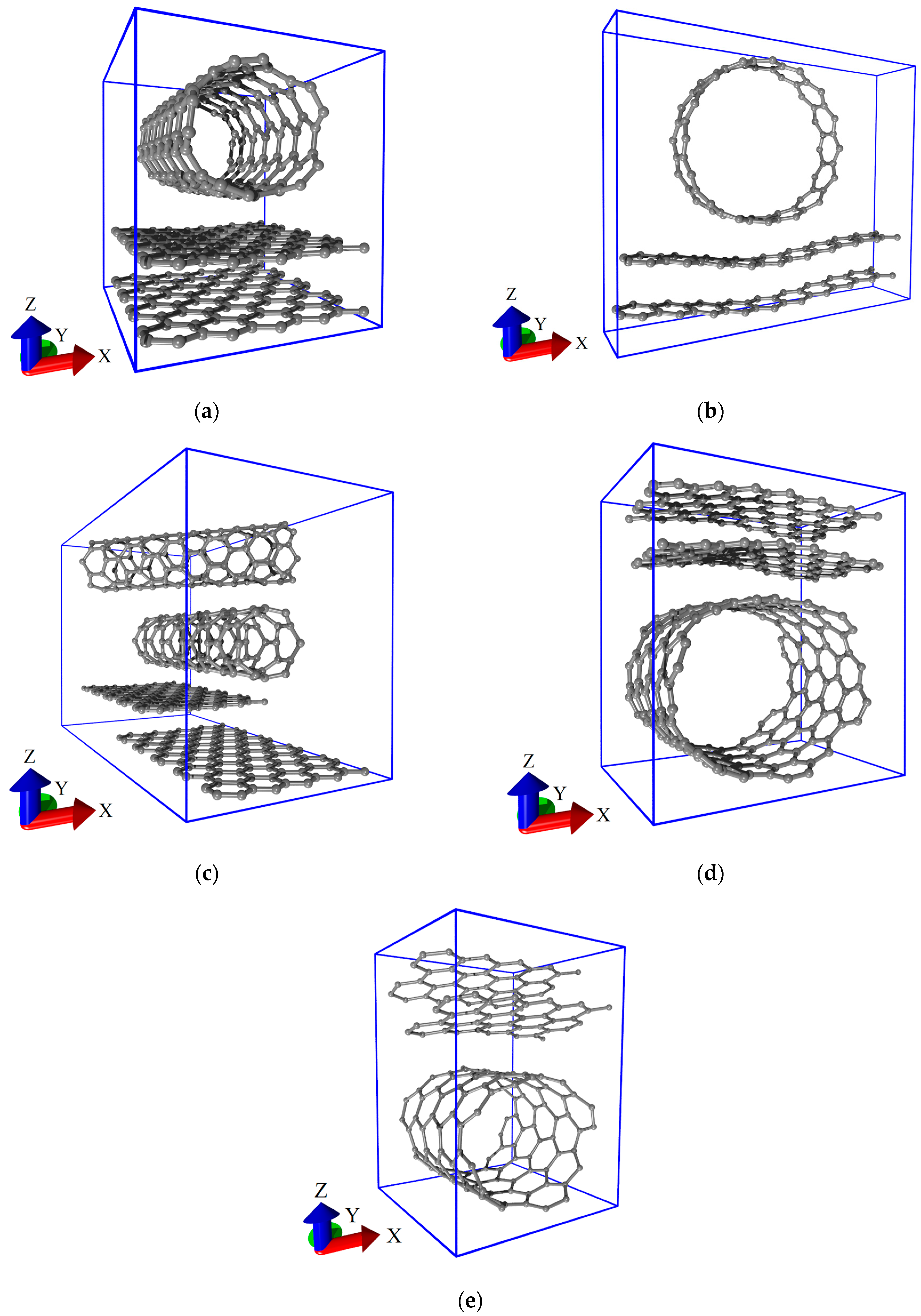
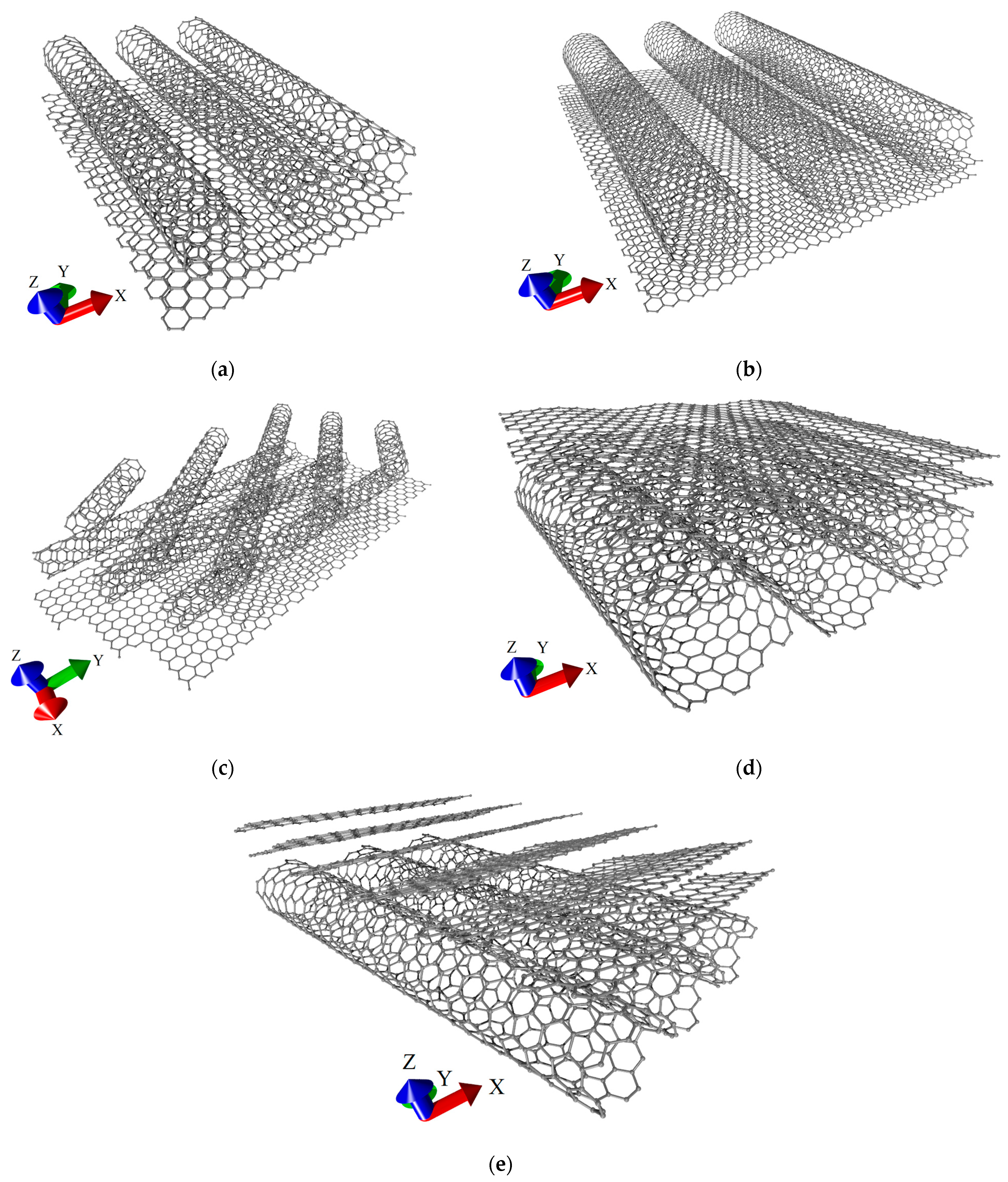
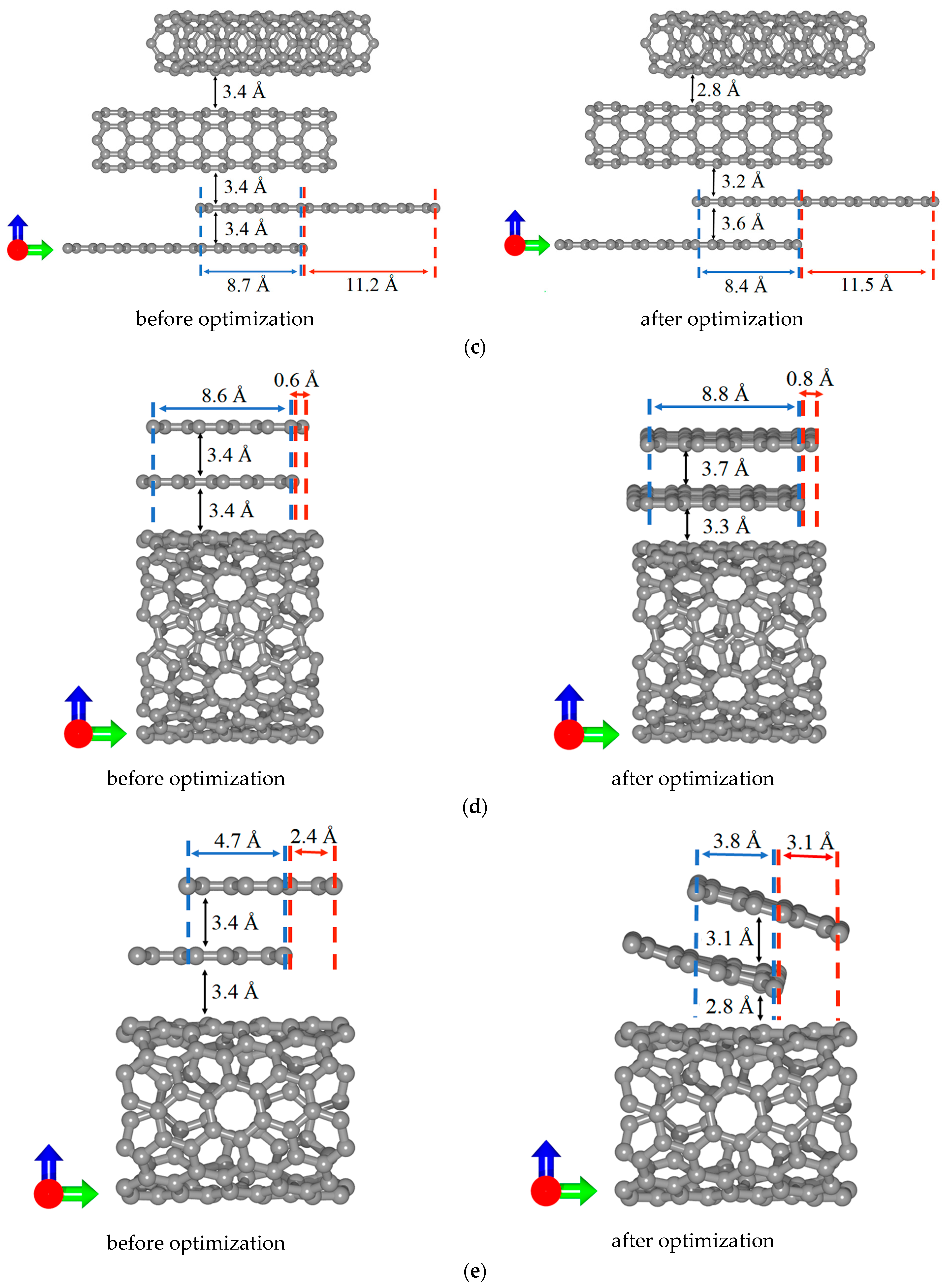
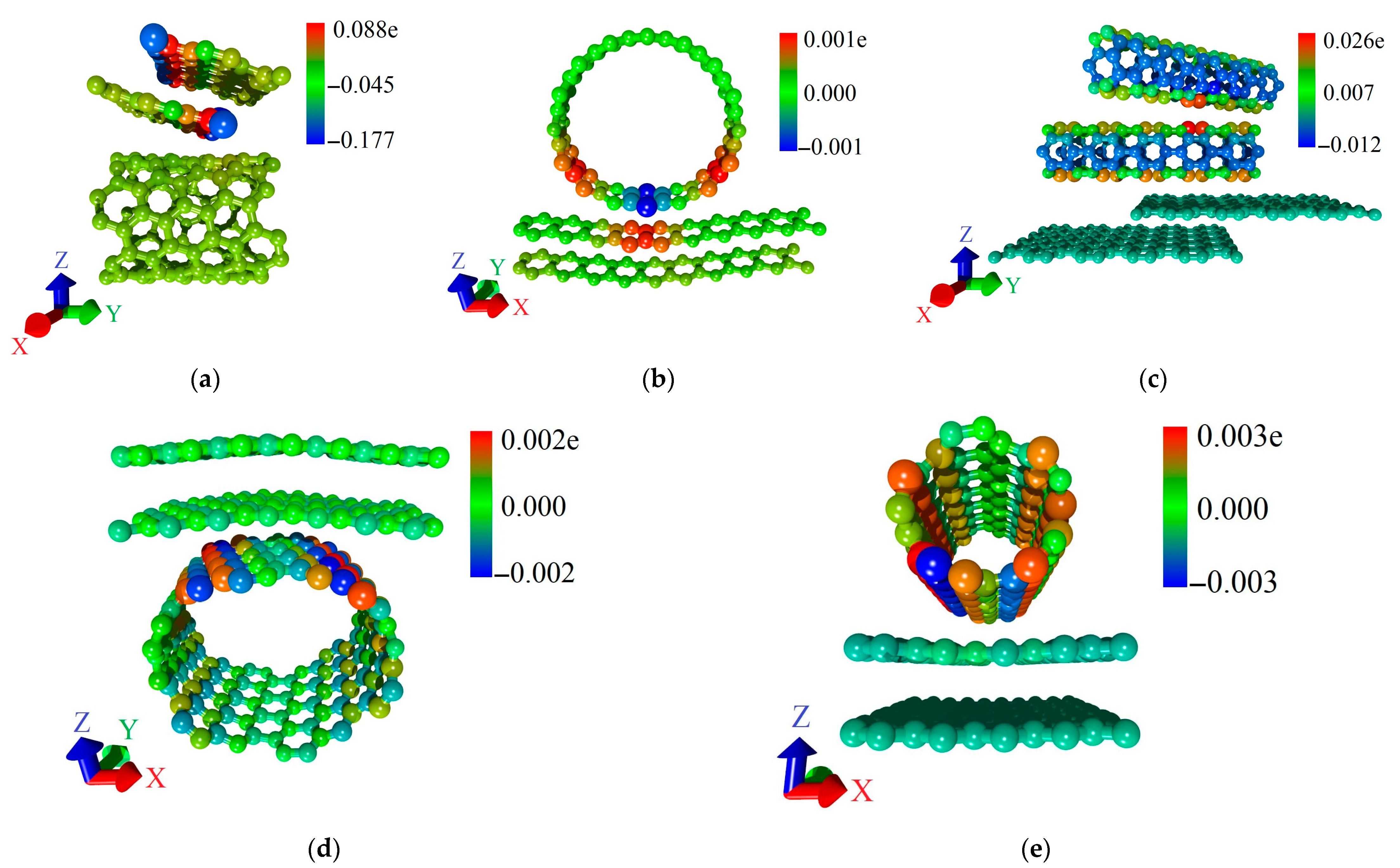
3.1. Atomistic Models of All-Carbon Films

In this study, five structural configurations of all-carbon films are considered. To form these configurations, nanotubes with chirality indices (5,5), (6,0), (16,0), (12,6), (8,4), and AA-/AB-stacked bilayer graphene were chosen. The above mentioned SWCNTs were selected based for the following reasons. Nanotubes with chirality indices (8,4), (12,6), and (16,0) with a diameter in the range of ~0.8–1.2 nm are widely synthesized high-purity (over 90%) SWCNTs [59,60]. Nanotubes with chirality indices (5,5) and (6,0) are well-tested model objects for studying the electronic properties of SWCNTs [61,62]. The use of (5,5) and (6,0) SWCNTs is also explained by the limitations on the sizes of the calculated supercells, which are imposed by high-precision quantum calculations. The choice of bilayer graphene is explained by its higher stability compared to single-layer graphene.
The relaxed structures of considered supercells are shown in Figure 2. The first structural configuration (V1) is formed by armchair (5,5) SWCNTs and AA-stacked bilayer graphene (see Figure 2a). The second structural configuration (V2) is formed by zigzag (16,0) SWCNTs and AA-stacked bilayer graphene (see Figure 2b). In the first two configurations, nanotubes are oriented in the “armchair” direction of the hexagonal graphene lattice (along the Y axis). The third structural configuration (V3) is represented by two layers of zigzag (6,0) SWCNTs located on AB-stacked bilayer graphene (see Figure 2c). The upper layer of SWCNTs is rotated relative to the lower one at an angle of 45⁰. The lower layer of SWCNTs is oriented along the “armchair” direction of the hexagonal graphene lattice. The fourth structural configuration (V4) is formed by (12,6) SWCNTs and AB-stacked bilayer graphene (see Figure 2d). Finally, the fifth structural configuration (V5) is formed by (8,4) SWCNTs and AB-stacked bilayer graphene (see Figure 2e). Unlike the first three configurations, the bilayer graphene in configurations V4 and V5 is located above the nanotube. The main difference between the structural configurations V4 and V5 is the orientation of the bilayer graphene with respect to the nanotube. In V5 configuration, the graphene layers are positioned at an acute angle to the nanotube, unlike V4 configuration, where both layers are located exactly above the nanotube. In structural configurations V3, V4, and V5, the nanotubes and graphene overlap, creating regions (“islands”) of increased carbon density in the graphene–SWCNT hybrid structure. In what follows, we will refer to this topology as an island-type topology. This is consistent with known experimental data [6]. For structural configurations V2, V4, and V5, the deformation of bilayer graphene and SWCNTs is observed. This is due to the larger diameter of SWCNTs and the smaller sizes of graphene fragments in the supercell compared to configurations V1 and V3. The consequence of this is a stronger mutual influence of the nanotube and graphene in the V2, V4, and V5 structural configurations. The extended fragments of all-carbon films are presented in Figure 3. These fragments were obtained as a result of translation of supercells shown in Figure 2 along the X and Y axes. Figure 3d,e clearly demonstrates the above-mentioned difference in the mutual orientation of SWCNTs and graphene fragments between structural configurations V4 and V5.
When constructing supercells of all-carbon films, an important issue was the formation of bilayer graphene with AA and AB stacking. Figure 4 shows the evolution of the atomic structure of bilayer graphene in all-carbon films during the optimization of supercells. Note that in the case of V5 structural configuration, the tilted position of bilayer graphene is precisely the result of searching for the most energy-efficient arrangement of graphene layers. Initially (before optimization), the graphene layers were located in the same plane as the nanotube. As a result of tilting the bilayer graphene, the shift between its layers also changed significantly: from 2.4 Å to 3.1 Å. The calculated values of the formation energy of bilayer graphene in the supercells of considered structural configurations were –6.5 eV for V1, –4.1 eV for V2, –10.7 eV for V3, –47.2 eV for V4, and –31 eV for V5. The negative values of the formation energy indicate the energetic stability of the formed graphene bilayers. At the same time, the structures of bilayer graphene with the AB-stacking are more stable than those with AA-stacking. It is also possible to see how the distance between the bilayer graphene and SWCNTs changed during optimization. Depending on the type of structural configuration, the equlibrium distance between bilayer graphene and SWCNTs varies in the range of 2.9–3.6 Å (V1—3.1 Å, V2—3.3 Å, V3—3.2 Å, V4—3.3 Å, V5—2.8 Å). Configuration V3 is characterized by the longest (8.4 Å) overlap region of bilayer graphene and SWCNT.
The optimized values of translation vectors of all-carbon film supercells (Lx and Ly) are given in Table 1. The energy stability of the constructed supercells was estimated by the value of binding energy Eb as
E b = E f E g r E t u b e / N
where Ef is the energy of all-carbon film, Egr is the energy of bilayer graphene, Etube is the nanotube energy, and N is the number of atoms in the supercell. Table 1 shows the Eb values.
According to the data in Table 1, each of the considered structural configurations of an all-carbon hybrid film is characterized by a negative Eb value. Therefore, the constructed supercells of all-carbon films are energetically stable.

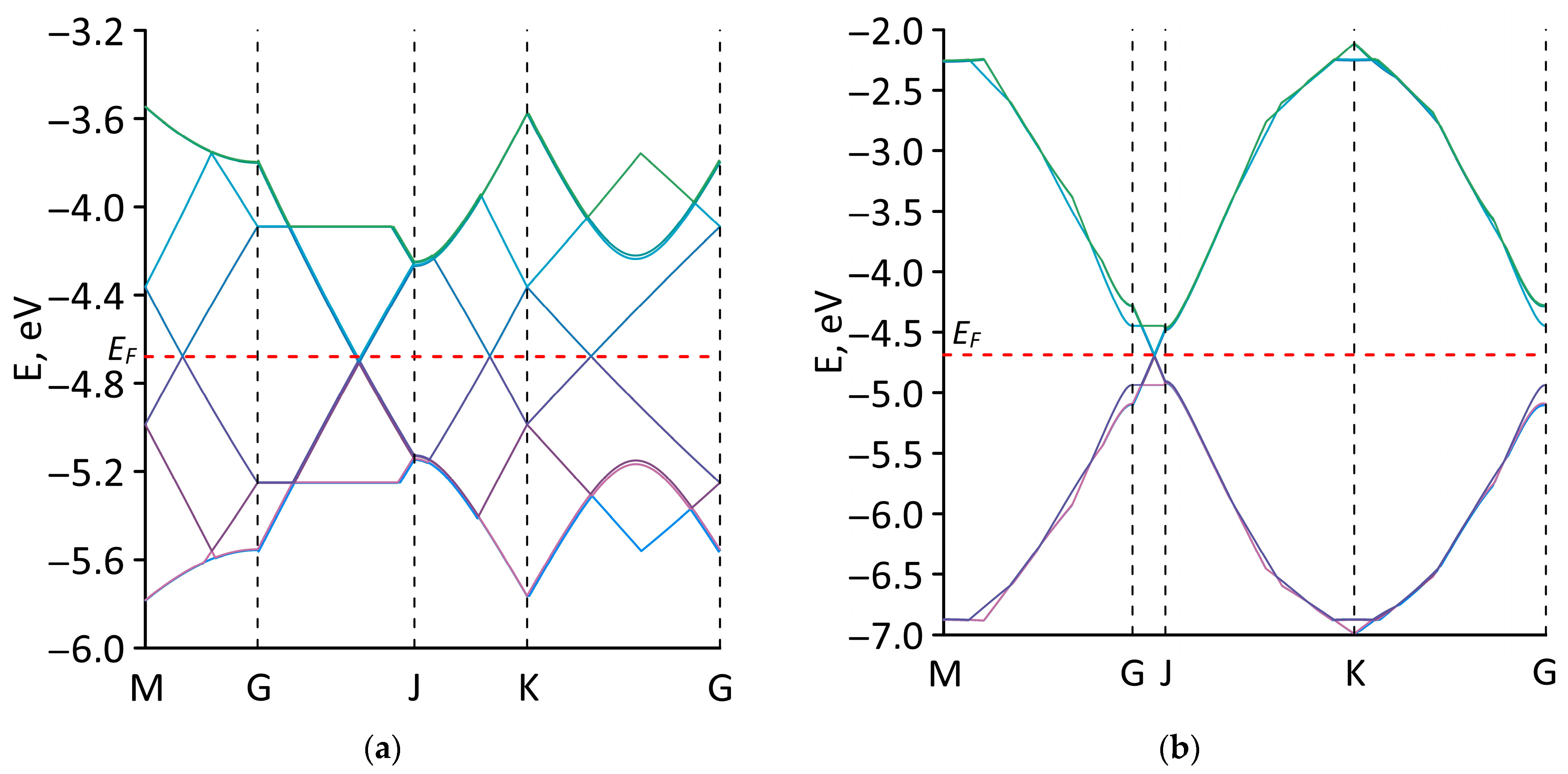
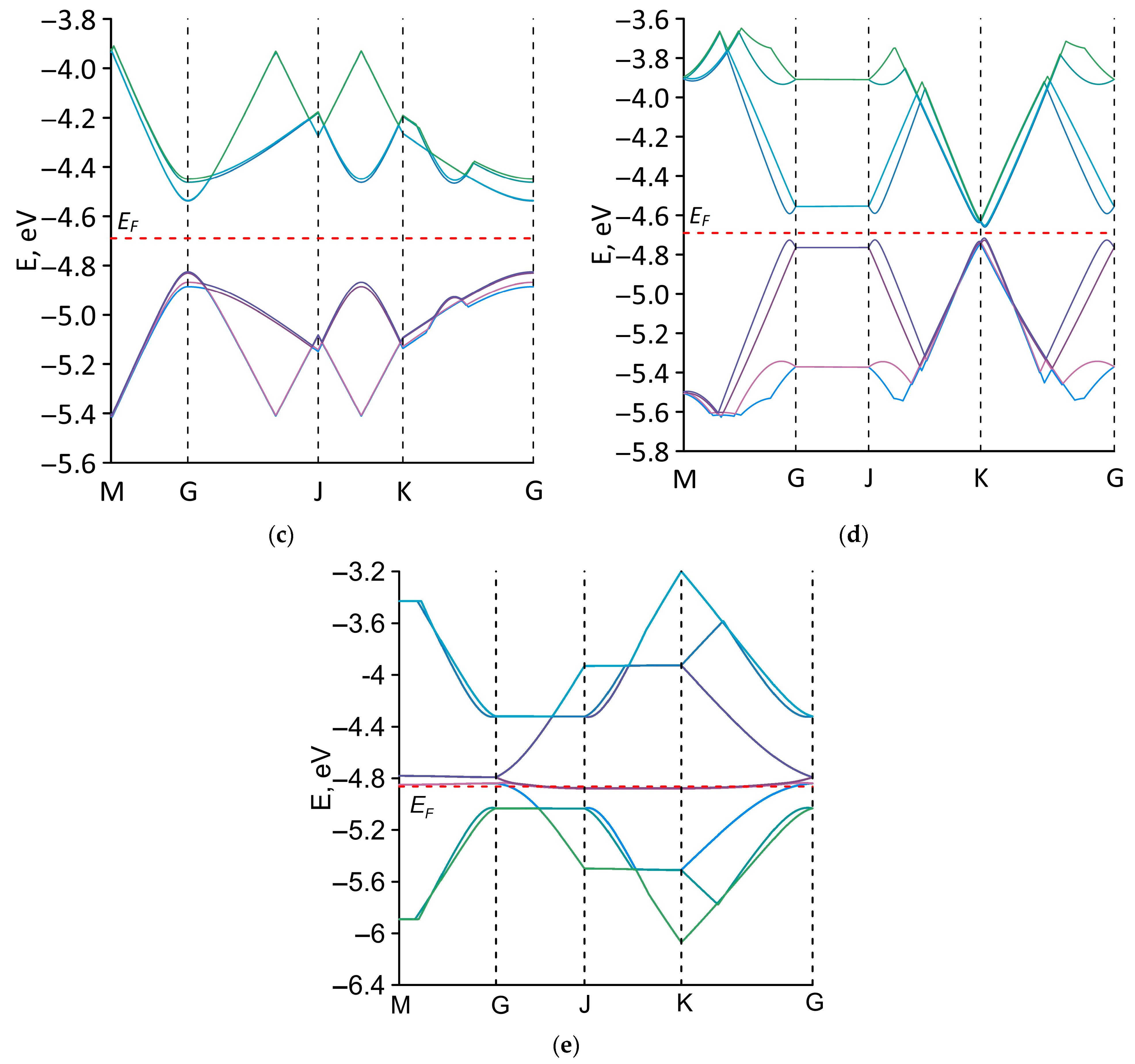
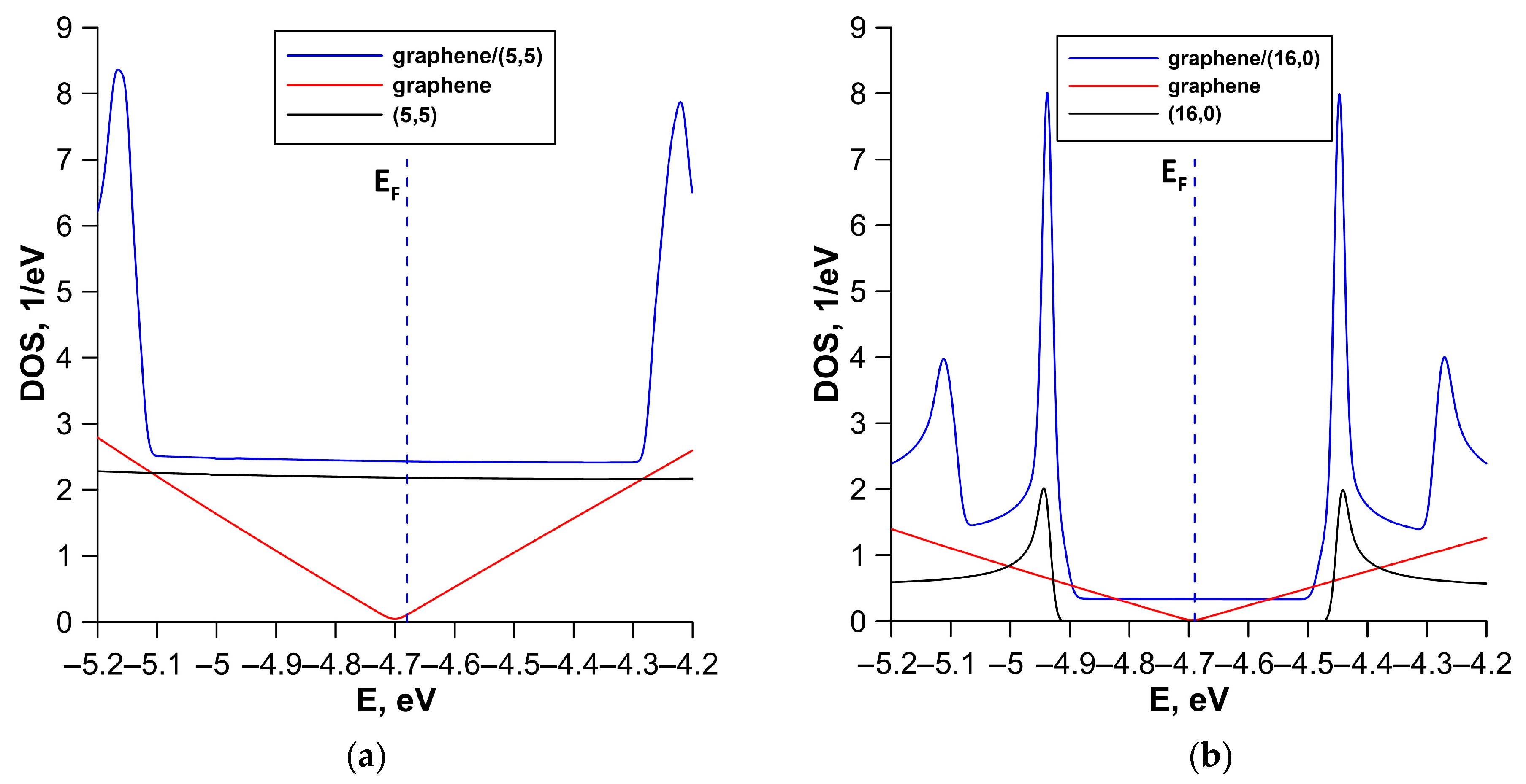
3.2. Electronic Properties of All-Carbon Films

To identify the features of the electronic properties of the studied all-carbon films, the band structure calculations using a basis of p-orbitals were carried out. The first Brillouin zone for all structural configurations of all-carbon films was rectangular. Figure 5 presents energy band diagrams of all-carbon films near the Fermi level EF. The EF values for each structural configuration of all-carbon films are given in Table 2. Configurations V1 (Figure 5a), V2 (Figure 5b), and V5 (Figure 5e) have a gapless band structure, which is typical for materials with a metallic conductivity. Configurations V3 and V4 have an energy gap in the band structure. The energy gap of the V3 configuration is several tenths of an electron volt (see Figure 5c). For the V4 configuration, the energy gap is insignificant and amounts to ~0.05 eV (see Figure 5d). The values of the energy gap Egap of all-carbon films are presented in Table 2.
To interpret the obtained energy band diagrams, we calculated the DOS distribution for each structural configuration. Our task was to establish the patterns of formation of the profile of DOS of all-carbon films. Figure 6 shows calculated DOS of all-carbon films and their components (individual SWCNT and bilayer graphene). Individual fragments of SWCNTs and bilayer graphene were cut from supercells of all-carbon films (see Figure 2). The gapless band structure of the V1 structural configuration is due to the metallic conductivity of both graphene and (5,5) SWCNT. In this case, the DOS profile of all-carbon film near the Fermi level EF completely repeats the DOS profile of the (5,5) SWCNT (see Figure 6a). The contours of the DOS profile of the V2 structural configuration largely repeat the contours of the DOS profile of the semiconductor (16,0) SWCNT (see Figure 6b). However, the gapless band structure of all-carbon film in this case is determined by the bilayer graphene, which is predominant in a quantitative ratio in the supercell of the V2 structural configuration. The semiconductor conductivity of the V3 structural configuration is attributed to the twisted structure of the SWCNT bilayer. The bilayer of (6,0) SWCNTs is characterized by an energy gap of 0.28 eV as is the graphene–(6,0) SWCNT film (see Figure 6c). A similar energy gap opening effect was previously established for twisted bilayer graphene [63]. The electronic structure of (12,6) SWCNT determines features of the electronic properties of V4 structural configuration. This is evidenced by the similarity of the profiles of DOS of (12,6) SWCNT and graphene–(12,6) SWCNT film (see Figure 5d). The small energy gap in the profile of DOS of graphene–(12,6) SWCNT film is caused by the deformation of (12,6) SWCNT during interaction with bilayer graphene. AB-stacked bilayer graphene plays a decisive role in the gapless band structure of the V5 structural configuration. The profile of DOS of AB-stacked bilayer graphene near the Fermi level completely repeats the contours of the profile of DOS of graphene–(8,4) SWCNT film. As is known, the electronic properties of a nanomaterial are determined precisely by the electronic states near the Fermi level. In addition, Table 2 shows that the Fermi level EF is –4.68 eV ÷ –4.69 eV for most of the considered structural configurations of all-carbon films, with the exception of V5. For this structural configuration, the Fermi level EF is –4.86 eV, as for the AB-packed bilayer graphene included in the graphene–(8,4) SWCNT film.
Thus, SWCNTs make a decisive contribution to the electronic structure of most of the considered structural configurations of all-carbon films. The V5 structural configuration is an exception. As noted above, the graphene layers are positioned at an angle relative to nanotube in this structural configuration (see Figure 3d). Moreover, the graphene layers have a finite width (three hexagons) along the Y axis and an infinitely extended along the X axis (nanoribbon-like structure). The V5 structural configuration is also characterized by the highest DOS near the Fermi level EF compared to other structural configurations. Moreover, the DOS peak values of the all-carbon hybrid film and its structural components coincide for the V5 structural configuration. Other structural configurations are characterized by an increase in DOS peaks of all-carbon films compared to the DOS of their structural components. This is caused by a synergistic effect of graphene and SWCNTs.

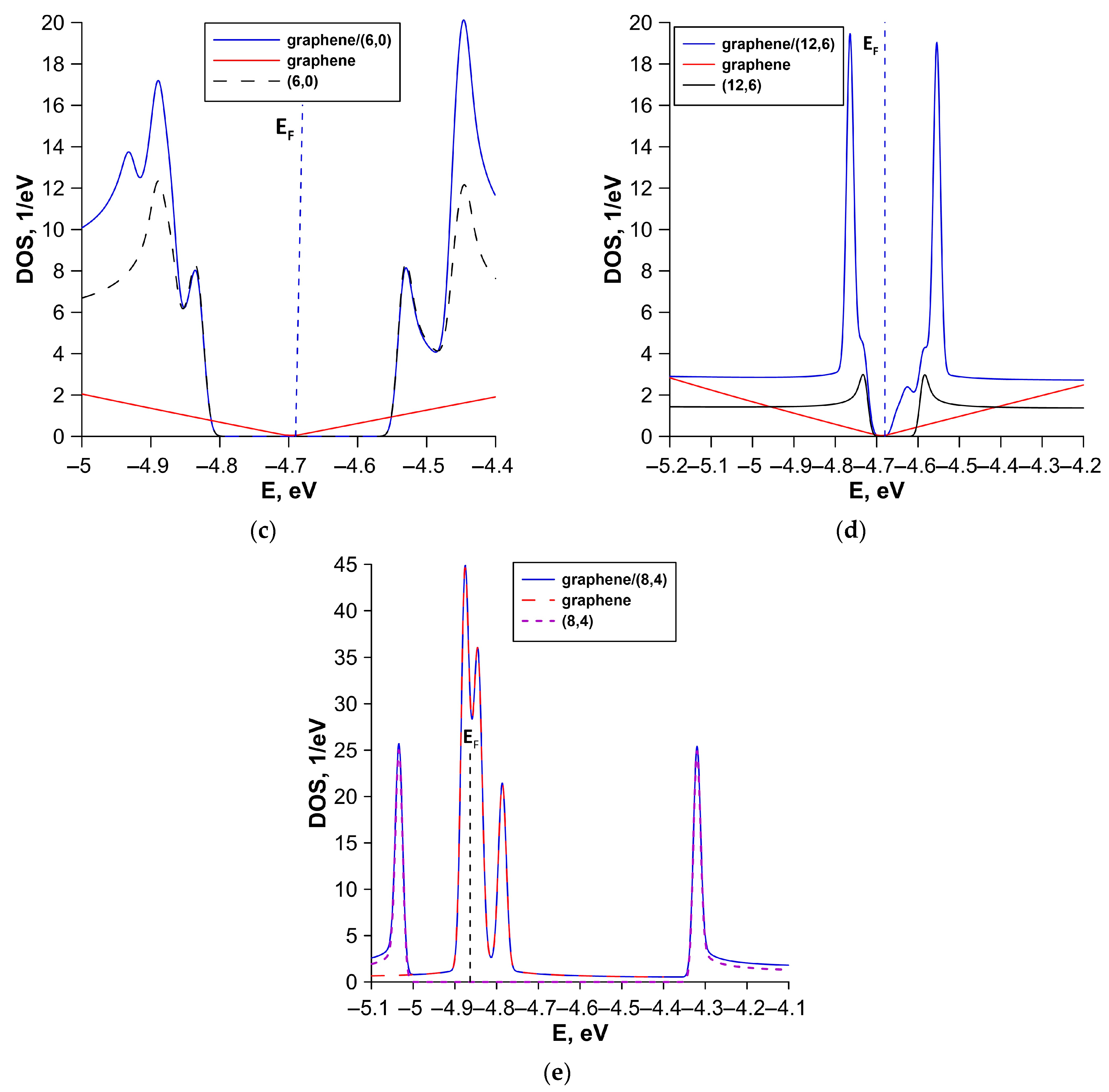
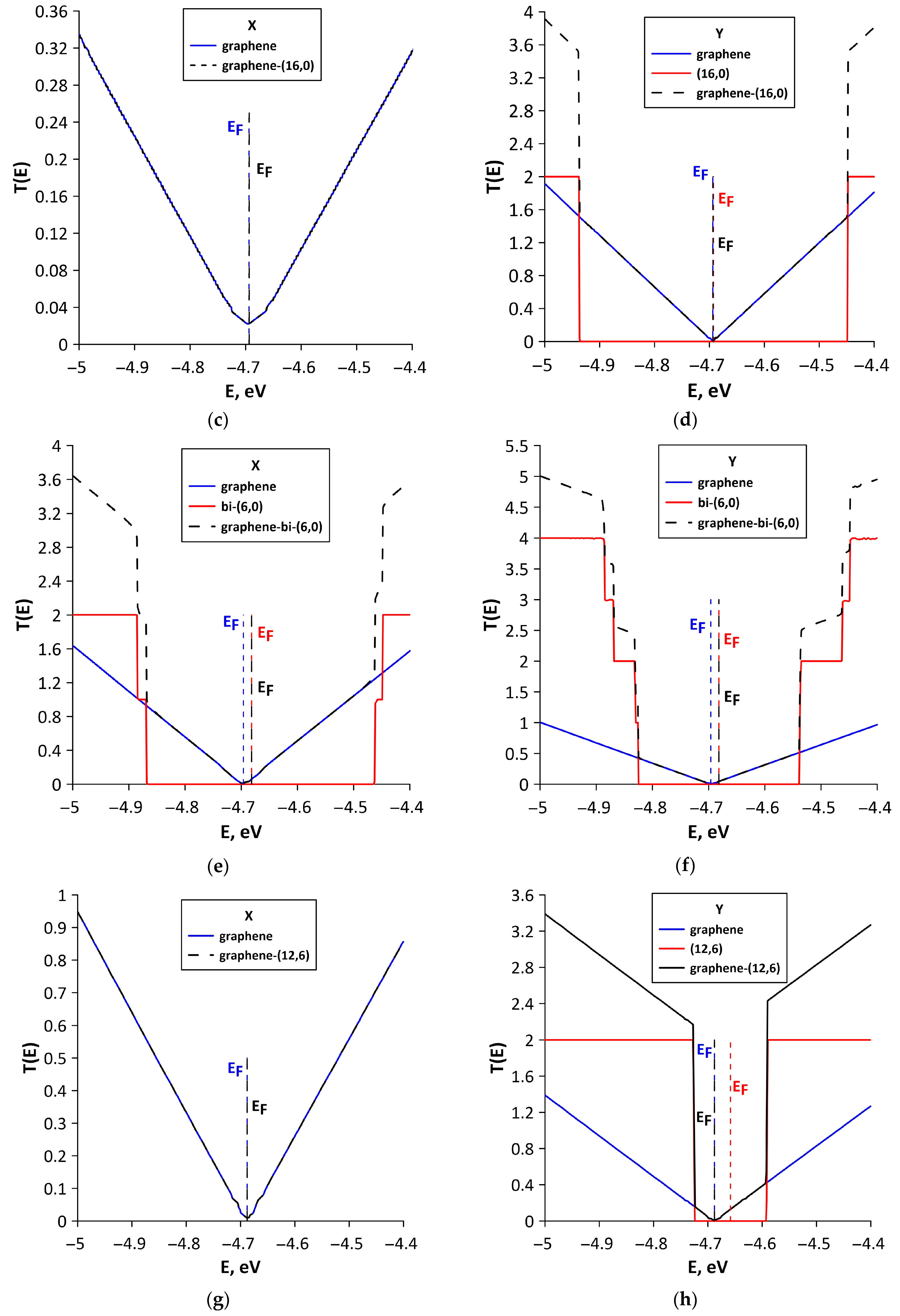
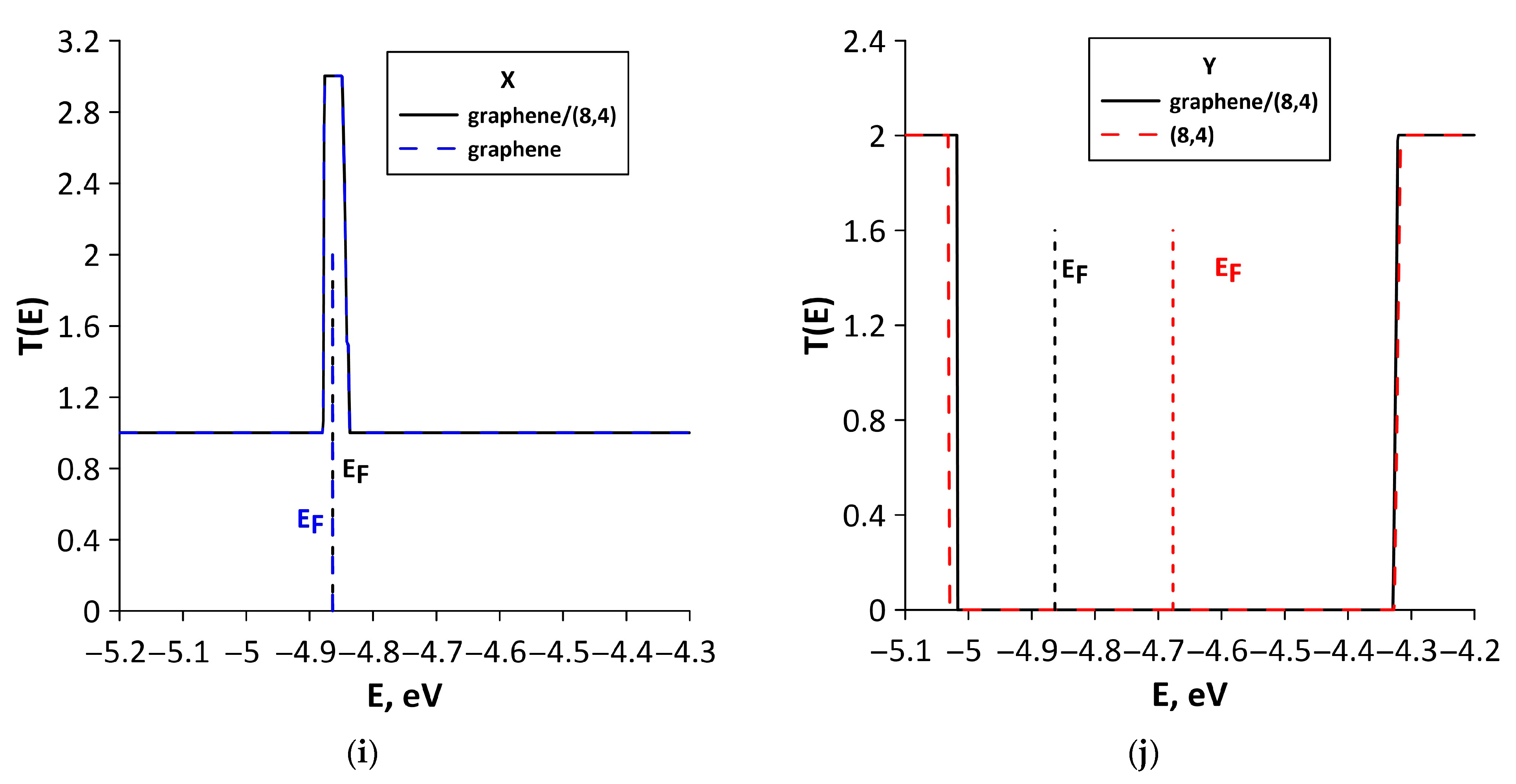
3.3. Electron Transport Properties of All-Carbon Films

Having identified the electronic structure features, we began to study electrical conductivity of considered all-carbon films. Table 3 presents the values of electrical resistances Rx and Ry of structural configurations V1, V2, V3, V4, and V5 in two directions of electron transport (see Section 2). Having analyzed the data in the table, one can note the anisotropy of the electrical conductivity of studied all-carbon films. Moreover, anisotropy manifests itself in different ways depending on geometric and topological features of all-carbon films. For structural configurations V1, V2, and V4, Rx is several times greater than Ry. For structural configurations V3 and V5, on the contrary, Ry is several times greater than Rx.
To explain the reasons for the observed anisotropy of electrical conductivity, we plotted graphs of the function T(E), called the transparency coefficient of the potential barrier. Figure 7 shows the T(E) graphs of studied all-carbon films for two directions of electron transport. For structural configurations V1 (Figure 7a), V2 (Figure 7b), and V4 (Figure 7d), the T(E) values near EF for electron transport along Y axis are several times greater than those along the X axis. That is, there are more conduction channels for electron transport in the direction of the Y axis. This explains the lower values of resistances Ry of these structural configurations. In turn, Figure 7c,e demonstrate that for structural configurations V3 and V5, the T(E) values near EF for electron transport along the X axis are greater than those along the Y axis. This difference is especially noticeable for V5 structural configuration. For this configuration, the T(E) takes a maximum value of three near EF for electron transport along the X axis. Along the Y axis, T(E) has a transport gap of ~0.7 eV.
To explain the differences in quantum transport of electrons between various structural configurations, we calculated T(E) functions of bilayer graphene and SWCNTs included in the supercells of all-carbon films. We also conducted a Mulliken population analysis (see Section 2), which characterizes the electronic charge distribution in graphene–SWCNT system. The T(E) plots of all-carbon films and their components (SWCNTs and bilayer graphene separately) for two directions of electron transport are presented in Figure 8. For structural configurations V1 (Figure 8a), V2 (Figure 8c), V4 (Figure 8g), and V5 (Figure 8i), the T(E) profile of all-carbon film completely coincides with T(E) profile of bilayer graphene fragment. Nanotubes in these configurations do not contribute to the formation of T(E) profile of all-carbon film, since T(E) of SWCNTs is equal to zero for electron transport along the X axis (perpendicular to nanotube axis). The highest T(E) value at EF for electron transport along the X axis is observed for the V5 structural configuration (Figure 8i). It contains bilayer graphene in the form of layers of finite width (3 hexagons) in the “armchair” direction but infinitely extended in the “zigzag” direction of hexagonal lattice (see Figure 3e). As is known, zigzag GNRs have a peak of T(E) at EF, which is due to presence of localized states EF [64]. AB-stacked bilayer graphene from the supercell of the V5 structural configuration also shows a DOS peak at EF (Figure 6e). Therefore, we can talk about the presence of graphene fragments like nanoribbons in the composition of the V5 structural configuration. It is also important to note the presence of charge transfer between AB-stacked bilayer graphene and (8,4) SWCNT during the formation of graphene–(8,4) SWCNT film. Mulliken population analysis showed that a partial charge of 0.1e is transferred from the (8,4) SWCNT to graphene (Figure 9a). This increases the electrical conductivity of bilayer graphene, and hence of graphene–(8,4) SWCNT film. Previously, the presence of charge transfer between SWCNT and graphene during their interaction was established experimentally [65]. The ability of graphene to exhibit charge transfer during interaction with various compounds has also been previously demonstrated experimentally [66]. The lowest values of T(E) for electron transport along the X axis are observed for structural configurations V2 and V4. For the V2 configuration, this can be explained by a rather noticeable deformation of the AA-stacked bilayer graphene as a result of interaction with (16,0) SWCNT (see Figure 2b). In addition, the bilayer graphene fragment included in the supercell of the V2 structural configuration is characterized by the lowest DOS near EF (see Figure 6b). Moreover, according to Mulliken population analysis, the semiconducting SWCNT (16,0) takes on a small amount (0.02 e) of partial charge from the graphene bilayer (Figure 9b). For the V4 configuration, there is also a deformation of the graphene layers as a result of interaction with the nanotube. However, there is almost no charge transfer between bilayer graphene and (12,6) SWCNT. According to Mulliken population analysis, a partial charge of only 0.007e is transferred from the nanotube to graphene (see Figure 9c). Mainly, the charge is redistributed between the graphene layers. The T(E) profile of the V3 structural configuration for electron transport along the X axis is formed by both the AB-stacked bilayer graphene and bilayer of (6,0) SWCNTs (Figure 8d). This is due to the fact that the nanotubes from the upper layer are turned relative to the nanotubes of the lower layer by 45° and partially participate in the formation of paths for the current flow in this direction of electron transport. The participation of (6,0) SWCNTs in the electron transport along the X axis is confirmed by the data of Mulliken population analysis (see Figure 9d). The partial charge of 0.1e is transferred from the bilayer of (6,0) SWCNTs to the bilayer graphene. The T(E) profile of graphene–(6,0) SWCNT film near EF (–4.681 ± 0.2 eV) is completely determined by the bilayer graphene. This is why the charge acquisition from the (6,0) SWCNT bilayer increases electrical conductivity of graphene-(6,0) SWCNT film.
The analysis of the T(E) curves for electron transport along the Y axis allows us to conclude that nanotubes make a significant contribution to the T(E) profile for studied structural configurations of all-carbon hybrid films. For the V1 (Figure 8b) and V5 (Figure 8j) structural configurations, the contribution of nanotubes is decisive to the T(E) profile. Let us consider these cases in more detail. For electron transport along the Y axis, the profile of T(E) of graphene–(5,5) SWCNT film follows the contours of T(E) of bilayer graphene, but the T(E) plot is shifted along the ordinate axis by two units. This is due to the influence of the (5,5) nanotube. It is conductive in this direction of electron transport and has a T(E) function equal to two over the entire energy range under consideration. Charge transfer also occurs between the bilayer graphene and (5,5) SWCNT. As a result, a partial charge of 0.14e is transferred from the (5,5) SWCNT to the bilayer graphene (Figure 9e). Since both AA-stacked bilayer graphene and (5,5) SWCNT exhibit metallic conductivity, the graphene–(5,5) SWCNT hybrid structure is characterized by the highest T(E) value for electron transport along the Y axis. As a consequence, the V1 configuration has the lowest electrical resistance Ry among the considered structural configurations of all-carbon hybrid films. During electron transport along the Y axis, the T(E) profile of graphene–(8,4) SWCNT film near EF (–4.863 eV) completely repeats the T(E) of (8,4) SWCNT, which has a transport gap of 0.7 eV. In this case, the bilayer graphene makes a minor contribution. As noted above, the supercell of the V5 structural configuration includes graphene fragments in the form of zigzag nanoribbons. They conduct current in the “zigzag” direction (X axis) of the hexagonal graphene lattice. In this regard, the V5 structural configuration has the lowest resistance Ry among the considered structural configurations of all-carbon films.
Thus, along with the conducting properties of bilayer graphene and SWCNTs, determined by their structural features, the mutual orientation of nanotubes and bilayer graphene plays an important role in the transport electronic properties of all-carbon films.

4. Conclusions

The influence of various topological features on the electronic transport properties of all-carbon films formed by bilayer graphene and SWCNTs was studied. The structural configurations of all-carbon films with topological features corresponding to known experimental data on the synthesis of graphene, SWCNTs, and their hybrids were considered. Configurations V3 and V5 can be considered the most promising structural configurations of all-carbon films from the perspective of topological control of their electronic transport properties, including the control of electrical conductivity anisotropy. The key structural feature of these configurations is the island-type topology. It is characterized by the presence of structural regions where nanotubes and graphene overlap, creating areas of increased carbon density. This topology is realized by AB-stacking in bilayer graphene and either by rotating the bilayer graphene relative to monolayer of nanotubes (V5 configuration) or by rotating one layer of nanotubes relative to the other when using a bilayer of nanotubes (V3 configuration). By creating regions with increased carbon density within all-carbon films, charge transfer is induced between bilayer graphene and nanotubes. The charge transferred to graphene from nanotubes increases electrical conductivity of the bilayer graphene. The twisted layers of nanotubes also cause the opening of the band gap in all-carbon films (structural configuration V3), which is important for their subsequent use in various electronics applications. By selecting the type of chirality of nanotubes (chiral or achiral) and the type of their conductivity (metallic or semiconductor), it is possible to both enhance and weaken the anisotropy of electrical conductivity in all-carbon films. In the case of the V5 structural configuration with (8,4) SWCNTs, the values of electrical resistances Rx and Ry differ by 37 times. In the case of the V3 structural configuration with (6,0) SWCNTs, Rx and Ry differ only by two times. The revealed patterns open up new possibilities in the design of nanoelectronic devices based on all-carbon films. In particular, these films can be used as anisotropic conductors, directional transistors, or nanoscale logic elements.

Author Contributions

Methodology, M.M.S. and O.E.G.; conceptualization, M.M.S. and O.E.G.; investigation, M.M.S., P.V.B. and O.E.G.; visualization, M.M.S. and P.V.B.; validation, M.M.S.; writing—original draft preparation, M.M.S. and P.V.B.; writing—review and editing, O.E.G. and M.M.S.; funding acquisition, M.M.S. All authors have read and agreed to the published version of the manuscript.

Funding

The research was funded by the grant of the Russian Science Foundation No. 24-79-10316, https://rscf.ru/project/24-79-10316/, accessed on 2 April 2025.

Data Availability Statement

The datasets presented in this article are not readily available because the data are part of an ongoing study.

Conflicts of Interest

The authors declare no conflicts of interest.

Abbreviations

The following abbreviations are used in this manuscript:
SCC-DFTBSelf-consistent charge density functional-based tight binding
CNTCarbon nanotube
SWCNTSingle-walled carbon nanotube
DOSDensity of states
GNRGraphene nanoribbon
MDMolecular dynamics
NEGFNonequilibrium Green’s functions

References

  1. Sheng, J.; Han, Z.; Jia, G.; Zhu, S.; Xu, Y.; Zhang, X.; Yao, Y.; Li, Y. Covalently Bonded Graphene Sheets on Carbon Nanotubes: Direct Growth and Outstanding Properties. Adv. Funct. Mater. 2023, 33, 2306785. [Google Scholar] [CrossRef]
  2. Zhao, X.; Qiu, L.; Kong, D.; Huang, Y.; Liu, J. Effects of Three-Dimensional Graphene–Carbon Nanotube Hybrid on the Mechanical Properties and Microstructure of Cement Paste. Materials 2023, 16, 6571. [Google Scholar] [CrossRef]
  3. Xia, K.; Zhan, H.; Gu, Y. Graphene and Carbon Nanotube Hybrid Structure: A Review. Procedia IUTAM 2017, 21, 94–101. [Google Scholar] [CrossRef]
  4. Zhu, Y.; Li, L.; Zhang, C.; Casillas, G.; Sun, Z.; Yan, Z.; Ruan, G.; Peng, Z.; Raji, A.R.O.; Kittrell, C.; et al. A seamless three-dimensional carbon nanotube graphene hybrid material. Nat. Commun. 2012, 3, 1225. [Google Scholar] [CrossRef]
  5. Ghosh, R.; Maruyama, T.; Kondo, H.; Kimoto, K.; Nagai, T.; Iijima, S. Synthesis of single-walled carbon nanotubes on graphene layers. Chem. Commun. 2015, 51, 8974–8977. [Google Scholar] [CrossRef] [PubMed]
  6. Kuang, J.; Dai, Z.; Liu, L.; Yang, Z.; Jinc, M.; Zhang, Z. Synergistic effects from graphene and carbon nanotubes endow ordered hierarchical structure foams with a combination of compressibility, super-elasticity and stability and potential application as pressure sensors. Nanoscale 2015, 7, 9252–9260. [Google Scholar] [CrossRef] [PubMed]
  7. Wang, R.; Hong, T.; Xu, Y.-Q. Ultrathin single-walled carbon nanotube network framed graphene hybrids. ACS Appl. Mater. Interfaces 2015, 7, 5233–5238. [Google Scholar] [CrossRef]
  8. Gbaguidi, A.; Namilae, S.; Kim, D. Synergy effect in hybrid nanocomposites based on carbon nanotubes and graphene nanoplatelets. Nanotechnology 2020, 31, 255704. [Google Scholar] [CrossRef]
  9. Du, W.; Ahmed, Z.; Wang, Q.; Yu, C.; Feng, Z.; Li, G.; Zhang, M.; Zhou, C.; Senegor, R.; Yang, C.Y. Structures, properties, and applications of CNT-graphene heterostructures. 2D Mater. 2019, 6, 042005. [Google Scholar] [CrossRef]
  10. Nguyen, D.D.; Tiwari, R.N.; Matsuoka, Y.; Hashimoto, G.; Rokuta, E.; Chen, Y.Z.; Chueh, Y.L.; Yoshimura, M. Low Vacuum Annealing of Cellulose Acetate on Nickel Towards Transparent Conductive CNT−Graphene Hybrid Films. ACS Appl. Mater. Interfaces 2014, 6, 9071–9077. [Google Scholar] [CrossRef]
  11. Liu, B.; Sun, J.; Zhao, J.; Yun, X. Hybrid graphene and carbon nanotube–reinforced composites: Polymer, metal, and ceramic matrices. Adv. Compos. Hybrid Mater. 2025, 8, 1. [Google Scholar] [CrossRef]
  12. Lan, M.; Jia, X.; Tian, R.; Feng, L.; Shao, D.; Song, H. Advancing multifunctional thermal management with multistate graphene/CNTs conjugated hybrids. Carbon 2024, 219, 118850. [Google Scholar] [CrossRef]
  13. Khosravifar, M.; Kondapalli, V.K.R.; Fang, Q.; Shanov, V. Graphene-CNT Hybrid Structures for Energy Storage Applications. In NanoCarbon: A Wonder Material for Energy Applications, 1st ed.; Gupta, R.K., Ed.; Springer: Singapore, 2024; Volume 2, pp. 17–40. [Google Scholar]
  14. Pyo, S.; Eun, Y.; Sim, J.; Kim, K.; Choi, J. Carbon nanotube-graphene hybrids for soft electronics, sensors, and actuators. Micro Nano Syst. Lett. 2022, 10, 9. [Google Scholar] [CrossRef]
  15. Qin, S.C.; Liu, Y.D.; Jiang, H.Z.; Xu, Y.; Shi, Y.; Zhang, R.; Wang, F. All-carbon hybrids for high-performance electronics, optoelectronics and energy storage. Sci. China Inf. Sci. 2019, 62, 220403. [Google Scholar] [CrossRef]
  16. Shi, E.; Li, H.; Yang, L.; Hou, J.; Li, Y.; Li, L.; Cao, A.; Fang, Y. Carbon nanotube network embroidered graphene films for monolithic all-carbon electronics. Adv. Mater. 2015, 27, 682–688. [Google Scholar] [CrossRef]
  17. John, J.P.; TE, M.N.; TK, B.S. A comprehensive review on the environmental applications of graphene–carbon nanotube hybrids: Recent progress, challenges and prospects. Mater. Adv. 2021, 2, 6816–6838. [Google Scholar] [CrossRef]
  18. Zakaria, M.R.; Omar, M.F.; Zainol Abidin, M.S.; Md Akil, H.; Abdullah, M.M.A.B. Recent progress in the three-dimensional structure of graphene-carbon nanotubes hybrid and their supercapacitor and high-performance battery applications. Compos.—A Appl. Sci. Manuf. 2022, 154, 106756. [Google Scholar] [CrossRef]
  19. Dang, V.T.; Nguyen, D.D.; Cao, T.T.; Le, P.H.; Tran, D.L.; Phan, N.M.; Nguyen, V.C. Recent trends in preparation and application of carbon nanotube–graphene hybrid thin films. Adv. Nat. Sci. Nanosci. Nanotechnol. 2016, 7, 033002. [Google Scholar] [CrossRef]
  20. Zhang, J.; Chen, Z.; Xu, X.; Liao, W.; Yan, L. A simple and efficient approach to fabricate graphene/CNT hybrid transparent conductive films. RSC Adv. 2017, 7, 52555–52560. [Google Scholar] [CrossRef]
  21. Cai, L.; Xue, X.; Liu, M.; Li, H.; Zhou, X.; Yu, G. One-step synthesis of seamless graphene-carbon nanotube heterojunctions by chemical vapor deposition. APL Mater. 2021, 9, 041110. [Google Scholar] [CrossRef]
  22. Chuc, N.V.; Thanh, C.T.; Tu, N.V.; Phuong, V.T.Q.; Thang, P.V.; Tam, N.T.T. A simple approach to the fabrication of graphene-carbon nanotube hybrid films on copper substrate by chemical vapor deposition. J. Mater. Sci. Technol. 2015, 31, 479–483. [Google Scholar] [CrossRef]
  23. Wu, X.; Mu, F.; Zhao, H. Recent progress in the synthesis of graphene/CNT composites and the energy-related applications. J. Mater. Sci. Technol. 2020, 55, 16–34. [Google Scholar] [CrossRef]
  24. Kim, S.H.; Song, W.; Jung, M.W.; Kang, M.A.; Kim, K.; Chang, S.J.; Lee, S.S.; Lim, J.; Hwang, J.; Myung, S.; et al. Carbon Nanotube and Graphene Hybrid Thin Film for Transparent Electrodes and Field Effect Transistors. Adv. Mater. 2014, 26, 4247–4252. [Google Scholar] [CrossRef] [PubMed]
  25. Lv, R.; Cruz-Silva, E.; Terrones, M. Building Complex Hybrid Carbon Architectures by Covalent Interconnections: Graphene-Nanotube Hybrids and More. ACS Nano 2014, 8, 4061–4069. [Google Scholar] [CrossRef]
  26. Kholmanov, I.N.; Magnuson, C.W.; Piner, R.; Kim, J.Y.; Aliev, A.E.; Tan, C.; Kim, T.Y.; Zakhidov, A.A.; Sberveglieri, G.; Baughman, R.H.; et al. Optical, electrical, and electromechanical properties of hybrid graphene/carbon nanotube films. Adv. Mater. 2015, 27, 3053–3059. [Google Scholar] [CrossRef]
  27. Li, L.; Li, H.; Guo, Y.; Yang, L.; Fang, Y. Direct synthesis of graphene/carbon nanotube hybrid films from multiwalled carbon nanotubes on copper. Carbon 2017, 118, 675–679. [Google Scholar] [CrossRef]
  28. Zhou, W.; Bai, X.; Wang, E.; Xie, S. Synthesis, Structure, and Properties of Single-Walled Carbon Nanotubes. Adv. Mater. 2009, 21, 4565–4583. [Google Scholar] [CrossRef]
  29. Yan, Z.; Peng, Z.; Casillas, G.; Lin, J.; Xiang, C.; Zhou, H.; Yang, Y.; Ruan, G.; Raji, A.R.O.; Samuel, E.L.G.; et al. Rebar graphene. ACS Nano 2014, 8, 5061–5068. [Google Scholar] [CrossRef]
  30. Gan, X.; Lv, R.; Bai, J.; Zhang, Z.; Wei, J.; Huang, Z.H.; Zhu, H.; Kang, F.; Terrones, M. Efficient photovoltaic conversion of graphene–carbon nanotube hybrid films grown from solid precursors. 2D Mater. 2015, 2, 034003. [Google Scholar] [CrossRef]
  31. Li, X.L.; Sha, J.W.; Lee, S.K.; Li, Y.L.; Ji, Y.S.; Zhao, Y.J.; Tour, J.M. Rivet graphene. ACS Nano 2016, 10, 7307–7313. [Google Scholar] [CrossRef]
  32. Liu, Y.; Wang, F.; Wang, X.; Wang, X.; Flahaut, E.; Liu, X.; Li, Y.; Wang, X.; Xu, Y.; Shi, Y.; et al. Planar carbon nanotube–graphene hybrid films for high-performance broadband photodetectors. Nat. Commun. 2015, 6, 8589. [Google Scholar] [CrossRef] [PubMed]
  33. Lin, X.; Liu, P.; Wei, Y.; Li, Q.; Wang, J.; Wu, Y.; Feng, C.; Zhang, L.; Fan, S.; Jiang, K. Development of an ultrathin film comprised of a graphene membrane and carbon nanotube vein support. Nat. Commun. 2013, 4, 2920. [Google Scholar] [CrossRef]
  34. Cai, B.; Yin, H.; Huo, T.; Ma, J.; Di, Z.; Li, M.; Hu, N.; Yang, Z.; Zhang, Y.; Su, Y. Semiconducting single-walled carbon nanotube/graphene van der Waals junctions for highly sensitive all-carbon hybrid humidity sensors. J. Mater. Chem. C 2020, 8, 3386–3394. [Google Scholar] [CrossRef]
  35. Kumar, P.; Woon, K.L.; Wong, W.S.; Saheed, M.S.M.; Burhanudin, Z.A. Hybrid film of single-layer graphene and carbon nanotube as transparent conductive electrode for organic light emitting diode. Synth. Met. 2019, 257, 116186. [Google Scholar] [CrossRef]
  36. Kim, H.; Kim, J.; Jeong, H.S.; Kim, H.; Lee, H.; Ha, J.M.; Choi, S.M.; Kim, T.H.; Nah, Y.C.; Shin, T.J.; et al. Spontaneous hybrids of graphene and carbon nanotube arrays at the liquid-gas interface for Li-ion battery anodes. Chem. Commun. 2018, 54, 5229–5232. [Google Scholar] [CrossRef] [PubMed]
  37. Hong, X.; Shi, W.; Zheng, H.; Liang, D. Effective carbon nanotubes/graphene hybrid films for electron field emission application. Vacuum 2019, 169, 108917. [Google Scholar] [CrossRef]
  38. Liu, Y.; Liu, Y.; Qin, S.; Xu, Y.; Zhang, R.; Wang, F. Graphene-carbon nanotube hybrid films for high-performance flexible photodetectors. Nano Res. 2017, 10, 1880–1887. [Google Scholar] [CrossRef]
  39. Wang, Z.; Li, J.; Yuan, K. Molecular dynamics simulation of thermal boundary conductance between horizontally aligned carbon nanotube and graphene. Int. J. Therm. Sci. 2018, 132, 589–596. [Google Scholar] [CrossRef]
  40. Panneerselvam, V.; Sathian, S.P. Thermal transport in a defective pillared graphene network: Insights from equilibrium molecular dynamics simulation. Phys. Chem. Chem. Phys. 2024, 26, 10650–10659. [Google Scholar] [CrossRef]
  41. Xu, T.; Jiang, J. On the Configuration of Graphene/Carbon Nanotube/Graphene Van der Waals Heterostructure. Phys. Chem. Chem. Phys. 2023, 25, 5066–5072. [Google Scholar] [CrossRef]
  42. Wei, L.; Zhang, L. Atomic Simulations of (8,0)CNT-Graphene by SCC-DFTB Algorithm. Nanomaterials 2022, 12, 1361. [Google Scholar] [CrossRef]
  43. Srivastava, J.; Gaur, A. Tight-binding investigation of the structural and vibrational properties of graphene–single wall carbon nanotube junctions. Nanoscale Adv. 2021, 3, 2030–2038. [Google Scholar] [CrossRef]
  44. Lepak-Kuc, S.; Milowska, K.Z.; Boncel, S.; Szybowicz, M.; Dychalska, A.; Jozwik, I.; Koziol, K.K.; Jakubowska, M.; Lekawa-Raus, A. Highly Conductive Doped Hybrid Carbon Nanotube–Graphene Wires. ACS Appl. Mater. Interfaces 2019, 11, 33207–33220. [Google Scholar] [CrossRef] [PubMed]
  45. Cook, B.G.; French, W.R.; Varga, K. Electron transport properties of CNT–graphene contacts. Appl. Phys. Lett. 2012, 101, 153501. [Google Scholar] [CrossRef]
  46. Srivastava, J.; Gaur, A. A tight-binding study of the electron transport through single-walled carbon nanotube-graphene hybrid nanostructures. J. Chem. Phys. 2021, 155, 244104. [Google Scholar] [CrossRef] [PubMed]
  47. Felix, A.B.; Pacheco, M.; Orellana, P.; Latgé, A. Vertical and In-Plane Electronic Transport of Graphene Nanoribbon/Nanotube Heterostructures. Nanomaterials 2022, 12, 3475. [Google Scholar] [CrossRef]
  48. Slepchenkov, M.M.; Glukhova, O.E. Mechanical and Electroconductive Properties of Mono- and Bilayer Graphene–Carbon Nanotube Films. Coatings 2019, 9, 74. [Google Scholar] [CrossRef]
  49. Elstner, M.; Seifert, G. Density functional tight binding. Phil. Trans. R. Soc. A 2014, 372, 20120483. [Google Scholar] [CrossRef]
  50. DFTB+. Density Functional Based Tight Binding (and More). Available online: https://dftbplus.org/ (accessed on 14 July 2021).
  51. Niehaus, T.A.; Melissen, S.T.A.G.; Aradi, B.; Allaei, S.M.V. Towards a simplified description of thermoelectric materials: Accuracy of approximate density functional theory for phonon dispersions. J. Phys. Condens. Matter 2019, 31, 395901. [Google Scholar] [CrossRef]
  52. Nair, M.N.; Palacio, I.; Celis, A.; Zobelli, A.; Gloter, A.; Kubsky, S.; Turmaud, J.; Conrad, M.; Berger, C.; de Heer, W.A.; et al. Band Gap Opening Induced by the Structural Periodicity in Epitaxial Graphene Buffer Layer. Nano Lett. 2017, 17, 2681–2689. [Google Scholar] [CrossRef]
  53. Wang, S.; Wu, L.; Wang, Z.; Qian, Z.; Liu, Y.; He, L.; Shen, L. Structure and electrical properties of double-walled silicon nanotubes depending on 585 defects and applied electric fields by SCC-DFTB method. Mater. Today Commun. 2024, 38, 108052. [Google Scholar] [CrossRef]
  54. Jing, L.; Zhao, D.; Lin, Z. Strain acting on adsorption of C60 onto graphene from DFTB algorithm. Carbon Trends 2021, 5, 100138. [Google Scholar] [CrossRef]
  55. Mulliken, R.S. Electronic Population Analysis on LCAO–MO MolecularWave Functions I. J. Chem. Phys. 1955, 23, 1833. [Google Scholar] [CrossRef]
  56. Zobelli, A.; Ivanovskaya, V.; Wagner, P.; Suarez-Martinez, I.; Yaya, A.; Ewels, C. A comparative study of density functional and density functional tight binding calculations of defects in graphene. Phys. Status Solidi B 2012, 249, 276–282. [Google Scholar] [CrossRef]
  57. Datta, S. Quantum Transport: Atom to Transistor, 2nd ed.; Cambridge University Press: New York, NY, USA, 2005; pp. 217–251. [Google Scholar]
  58. Glukhova, O.E.; Shmygin, D.S. The electrical conductivity of CNT/graphene composites: A new method for accelerating transmission function calculations. Beilstein J. Nanotechnol. 2018, 9, 1254–1262. [Google Scholar] [CrossRef]
  59. Zhang, S.; Kang, L.; Wang, X.; Tong, L.; Yang, L.; Wang, Z.; Qi, K.; Deng, S.; Li, Q.; Bai, X.; et al. Arrays of horizontal carbon nanotubes of controlled chirality grown using designed catalysts. Nature 2017, 543, 234–238. [Google Scholar] [CrossRef]
  60. Yang, F.; Wang, X.; Zhang, D.; Qi, K.; Yang, J.; Xu, Z.; Li, M.; Zhao, X.; Bai, X.; Li, Y. Growing Zigzag (16,0) Carbon Nanotubes with Structure-Defined Catalysts. J. Am. Chem. Soc. 2015, 137, 8688–8691. [Google Scholar] [CrossRef]
  61. Correa, J.D.; Florez, E.; Mora-Ramos, M.E. Ab initio study of hydrogen chemisorption in nitrogen-doped carbon nanotubes. Phys. Chem. Chem. Phys. 2016, 18, 25663–25670. [Google Scholar] [CrossRef]
  62. Sahu, R.K.; Mukherjee, V.; Dash, T.; Padhan, S.K.; Nayak, B.B. Vibrational and electronic properties of (5,0) zigzag and (5,5) armchair carbon and SiC nanotubes using density functional theory. Phys. B Condens. Matter. 2021, 615, 413074. [Google Scholar] [CrossRef]
  63. Symalla, F.; Shallcross, S.; Beljakov, I.; Fink, K.; Wenzel, W.; Meded, V. Band-gap engineering with a twist: Formation of intercalant superlattices in twisted graphene bilayers. Phys. Rev. B 2015, 91, 205412. [Google Scholar] [CrossRef]
  64. Zhang, L.; Zhao, J.; Cheng, N.; Chen, Z. Intrinsic electronic and transport properties of graphene nanoribbons with different widths. Phys. Chem. Chem. Phys. 2020, 22, 3584–3591. [Google Scholar] [CrossRef] [PubMed]
  65. Liu, Y.; Wang, F.; Liu, Y.; Wang, X.; Xu, Y.; Zhang, R. Charge transfer at carbon nanotube-graphene van der Waals heterojunctions. Nanoscale 2016, 8, 12883–12886. [Google Scholar] [CrossRef] [PubMed]
  66. Murali, A.; Sampath, S.; Appukutti Achuthan, B.; Sakar, M.; Chandrasekaran, S.; Suthanthira Vanitha, N.; Joseph Bensingh, R.; Abdul Kader, M.; Jaisankar, S.N. Copper (0) Mediated Single Electron Transfer-Living Radical Polymerization of Methyl Methacrylate: Functionalized Graphene as a Convenient Tool for Radical Initiator. Polymers 2020, 12, 874. [Google Scholar] [CrossRef] [PubMed]
Figure 1. Device structure as a channel enclosed between two electrodes as part of graphene–SWCNT (16,0) all-carbon film for calculating electron transport along X (a) and Y axes (b). The left (L) and right (R) electrodes are blue. The channel is gray.
Crystals 15 00445 g001
Figure 2. Equilibrium configurations of supercells of various types of structural configurations of all-carbon films: (a) V1; (b) V2; (c) V3; (d) V4; and (e) V5.
Crystals 15 00445 g002
Figure 3. Extended fragments of various types of structural configurations of all-carbon films: (a) V1; (b) V2; (c) V3; (d) V4; and (e) V5.
Crystals 15 00445 g003
Figure 4. Side view of supercells of various types of structural configurations of all-carbon films before and after optimization: (a) V1; (b) V2; (c) V3; (d) V4; and (e) V5. The green and blue arrows represent the X and Y axes respectively.
Crystals 15 00445 g004aCrystals 15 00445 g004b
Figure 5. Electronic band structures along the high-symmetry path in the first Brillouin zone for various types of structural configurations of all-carbon films: (a) V1; (b) V2; (c) V3; (d) V4; and (e) V5.
Crystals 15 00445 g005aCrystals 15 00445 g005b
Figure 6. DOS of various types of structural configurations of all-carbon films: (a) V1; (b) V2; (c) V3; (d) V4; and (e) V5. The vertical dotted line marks the Fermi level EF of all-carbon film.
Crystals 15 00445 g006aCrystals 15 00445 g006b
Figure 7. Transmission function T(E) of various types of structural configurations of all-carbon films: (a) V1; (b) V2; (c) V3; (d) V4; and (e) V5. The vertical dotted line denotes the Fermi level of all-carbon films.
Crystals 15 00445 g007aCrystals 15 00445 g007b
Figure 8. The patterns of formation of the T(E) profile of various types of structural configurations of all-carbon films for electron transport along X and Y axes: (a,b) V1; (c,d) V2; (e,f) V3; (g,h) V4; and (i,j) V5. The vertical dotted lines denote the Fermi level of all-carbon film (black color), bi-layer graphene (blue color), and nanotube (red color).
Crystals 15 00445 g008aCrystals 15 00445 g008bCrystals 15 00445 g008c
Figure 9. Distribution of partial Mulliken charge over atoms of supercell of various types of structural configurations of all-carbon films: (a) V5; (b) V2; (c) V3; (d) V4; and (e) V1.
Crystals 15 00445 g009
Table 1. Metric and energy characteristics of supercells of various types of structural configurations of all-carbon films.
CharacteristicsV1V2V3V4V5
Number of atoms300144440308192
Translation vectors, ÅLx = 12.35
Ly = 17.25
Lx = 24.63
Ly = 4.29
Lx = 12.38
Ly1 = 4.25,
Ly2 = 21.47
Lx = 17.07
Ly = 11.10
Lx = 12.3
Ly = 11.27
Eb, eV/atom–0.11–0.33–0.1–0.14–0.18
Table 2. Electron-energy characteristics of various types of structural configurations of all-carbon films.
CharacteristicsV1V2V3V4V5
EF, eV–4.684–4.693–4.681–4.687–4.863
Egap, eV0.000.000.280.050.00
Table 3. Electrical resistances Rx and Ry of various types of structural configurations of all-carbon films.
CharacteristicsV1V2V3V4V5
Rx, kOhm77.26265.3167.91128.167.38
Ry, kOhm5.7755.28177.3822.99262.63
Disclaimer/Publisher’s Note: The statements, opinions and data contained in all publications are solely those of the individual author(s) and contributor(s) and not of MDPI and/or the editor(s). MDPI and/or the editor(s) disclaim responsibility for any injury to people or property resulting from any ideas, methods, instructions or products referred to in the content.

