Article

Sm3+-Doped Bismuth(III) Oxosilicate (Bi4Si3O12:Sm3+): A Study of Crystal Structure and Mulliken Charges

1
College of Electric and Information Engineering, North Minzu University, Wenchang Road 204, Yinchuan 750021, China
2
Key Laboratory of Physics and Photoelectric Information Functional Materials Sciences and Technology, North Minzu University, Wenchang Road 204, Yinchuan 750021, China
3
Microelectronics and Solid-State Electronics Device Research Center, North Minzu University, Yinchuan 750021, China
4
Ningxia Ju Jing Yuan Crystal Technology Company Limited, Shizuishan 753000, China
5
School of Materials Science and Engineering, Shanghai Institute of Technology, Haiquan Road, Shanghai 201418, China
*
Authors to whom correspondence should be addressed.
Crystals 2025, 15(5), 423; https://doi.org/10.3390/cryst15050423
Submission received: 18 March 2025 / Revised: 28 April 2025 / Accepted: 29 April 2025 / Published: 30 April 2025

Abstract

:
In this paper, using the Materials Studio software (version 2020) and based on first-principles and density functional theory, the effects of Sm3+ doping at different ratios (1/12, 1/6, and 1/3) on the crystal structure and Mulliken charge distribution of bismuth silicate (Bi4Si3O12, BSO) were analyzed. The examination of the crystal framework and Mulliken charge allocation reveals that increasing levels of Sm3+ doping have the potential to warp the lattice’s symmetry and result in a decrease in electrical conductivity. With the rise in the concentration of Sm3+ doping, the Sm-O bond length shows a pattern of a rise at first and then a fall, demonstrating that electrons are shared, and reaches its minimum length with a doping proportion of 1/12. At the same time, when the doping concentration of Sm3+ rises, the Bi-O bond length becomes longer; it reaches its shortest length when the doping concentration is 1/12. This finding suggests that when a small quantity of Sm3+ is doped, especially when the doping concentration is 1/12, the covalent nature of the bonds between Sm-O and Bi-O atoms within the BSO crystal is strengthened.

1. Introduction

Scintillator materials, also known as scintillating materials, are substances capable of transforming a small portion of the energy from incident ionizing radiation into photons with low energy levels. They serve as a crucial element within scintillation detectors [1], particularly being of great importance for rapid time measurement in the field of nuclear physics, precise energy measurement in high-energy physics, and medical techniques such as positron emission tomography (PET) [2]. Bismuth silicate (Bi4Si3O12, BSO) crystals are considered an excellent new type of scintillating material [3].
The BSO (bismuth silicate) crystal belongs to the cubic system [3], with cubic symmetry, and its space group is I-43d [4]. In this structure, bismuth (Bi), silicon (Si), and oxygen (O) atoms occupy the 16c, 12a, and 48e positions, respectively (using Wyckoff notation). The Bi3+ ion is coordinated with six [SiO4] tetrahedra through shared oxygen atoms, forming a distorted octahedron [BiO6] with sixfold oxygen coordination [5]. Our research group [6] used an improved vertical Bridgeman method to grow BSO:RE (RE = Eu3+, Sm3+, Ho3+, Tb3+) crystals and studied the effects of doping on scintillation performance, which showed that lower concentrations of Sm3+ doping can improve scintillation performance, and the doping radius of rare-earth ions is an important factor affecting the scintillation performance of BSO crystals. BSO crystals have been proven to be a good host for the doping of trivalent lanthanide ions, and the outstanding electro-optic characteristics of RE3+-doped BSO crystals position them as a highly promising material for applications in optical amplifiers [7,8] or versatile optical laser devices [9]. M.V. Lalic et al. [10] conducted a first-principles study on pure BSO crystals, taking into account the complete atomic lattice arrangement and examining their optical properties in relation to the energy of incoming radiation, revealing the light absorption mechanism of BSO crystals. The findings revealed that O atoms are of vital importance in absorbing the energy of incoming radiation and in the shift to Bi ions, which act as the core component in the luminescence process of this material. Overall, while experiments have demonstrated that the scintillation performance of BSO can be enhanced by a small amount of rare-earth doping, this is of great significance for fields such as radiation detection and medical imaging. However, the study of rare-earth doping at the microscopic level still lacks a theoretical mechanism [11]. This research is targeted at providing theoretical groundwork for the implementation of rare-earth-doped BSO by deeply analyzing the impact of rare-earth-element ion Sm3+ doping on the crystal structure and electronic characteristics of BSO through first-principles calculations. In previous studies, Guo K et al. [12] used first-principles calculation methods to investigate the stability of the structure, chemical bonding, Mulliken population distribution, and charge density characteristics of REZnOSb (RE = La-Nd, Sm-Gd). They observed that the unit cell parameters derived from the Generalized Gradient Approximation (GGA) aligned more closely with experimental data compared to those obtained from the Local Density Approximation (LDA). Additionally, chemical bond analysis indicated significant polar covalent interactions among the atoms involved. Yue S et al. [13] employed density functional theory (DFT) to study the interactions between rare-earth atoms (La, Nd, Sm, and Eu) and single-walled carbon nanotubes (SWCNTs) ((6,0) and (8,0)). Through Mulliken analysis, they revealed strong interactions between rare-earth atoms and carbon nanotubes. Yanjun Qin et al. [14] used first-principles methods and density functional theory, and through Mulliken decomposition and differential charge density analysis, they discovered that as the lattice constant increased, the charge transferred from Si atoms to C atoms and the number of N atoms decreased; in addition, the covalency between Si-C and Si-N atoms weakened, further demonstrating how doping affects the electronic structure of materials. Our research group [15] used first-principles methods to dope materials with different proportions of Eu3+, and it was shown through the results that as the doping ratio of Eu3+ increased, the covalency between Eu-O and Bi-O atoms was strengthened once the Eu3+ doping concentration reached 1/3. These studies provide important insights into the role of doping ions on the polarity between atoms. However, research on the charge transfer and changes caused by doping ions is still limited. Based on the aforementioned studies, this article employs first-principles calculations using the Virtual Crystal Approximation (VCA) method [16] to compute and analyze the structure and Mulliken charge distribution of BSO crystals incorporating varying concentrations of Sm3+. By deeply analyzing the charge transfer and electronic structure changes induced by doping, the objective of this study is to provide new theoretical insights into the performance improvement of rare-earth-doped BSO.

2. Computational Methods

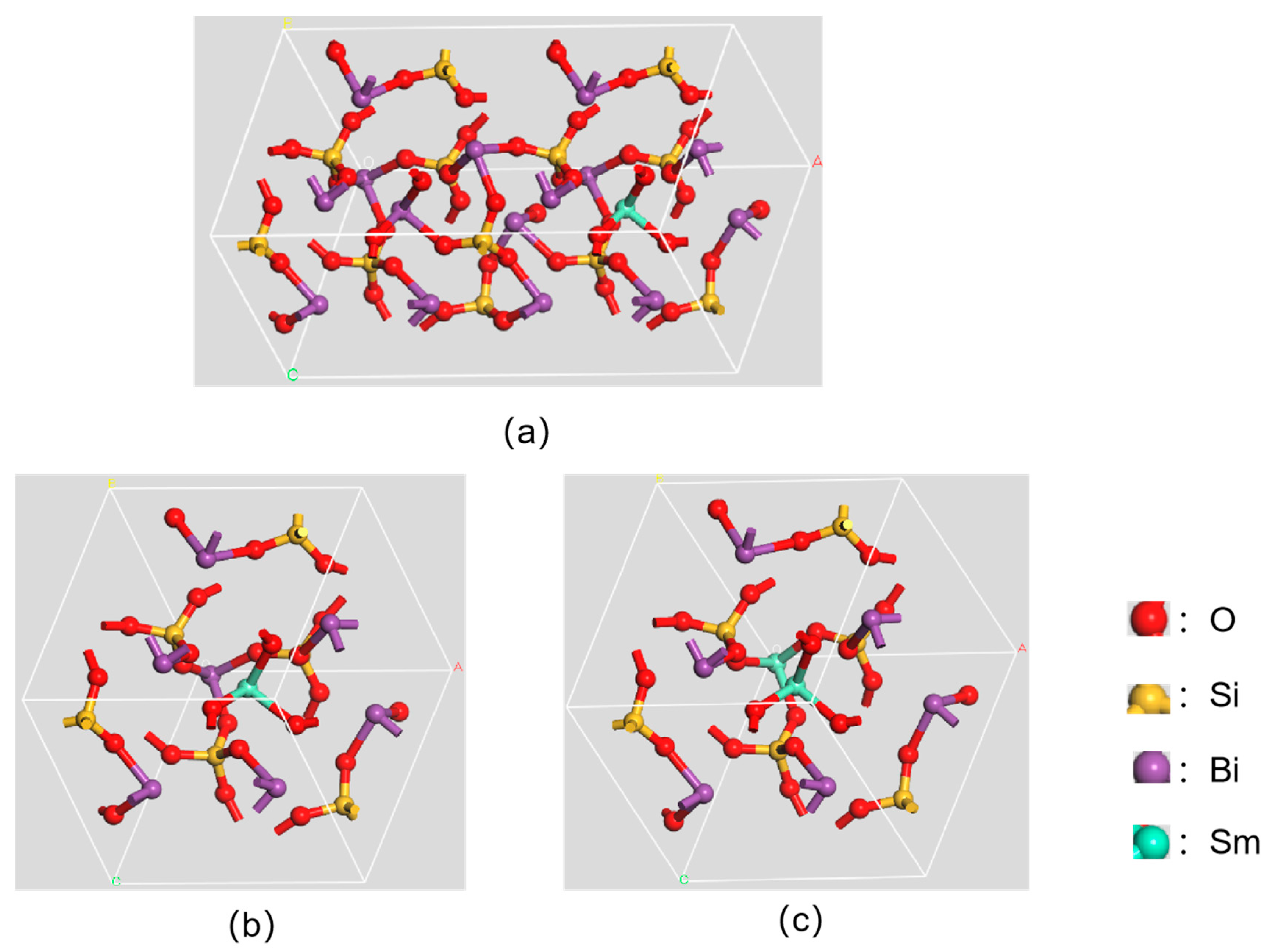
2.1. Setting Up a Structural Model

The crystal model constructed in this paper is based on an expanded 3 × 3 × 3 BSO supercell, and doping is carried out by replacing atoms. The ionic radius of Sm3+ is 96.4 pm, which is slightly smaller than that of Bi3+ (108 pm). As a result, Sm3+ has a higher probability of being substituted with Bi3+ within the lattice, as depicted in Figure 1a–c. In the lattice, Bi atoms are replaced by Sm atoms at ratios of 1/12, 1/6, and 1/3, respectively. In the figure, the doped Sm atoms are colored green, Bi atoms are purple, Si atoms are yellow, and O atoms are red. Figure 1a displays the chemical composition of Bi15SmSi12O48, Figure 1b displays the chemical composition of Bi7SmSi6O24, and Figure 1c shows the chemical composition of Bi6Sm2Si6O24.
Table 1 provides the cell parameters of Sm3+-doped bismuth silicate crystals at different doping ratios, including lattice constants (a, b, c) and lattice angles ( α , β , γ ). The values of the a-, b-, and c-axes vary with different doping ratios. For instance, when the doping ratio increases from 1/12 to 1/6, there is a significant decrease in the length of the a-axis and an increase in the lengths of the b- and c-axes; from 1/6 to 1/3, the changes in axis lengths become more gradual. This indicates that doping causes the cell to expand and contract in different directions, possibly due to differences in ionic radii and charge between Sm ions and the replaced Bi ions, leading to changes in the forces between ions and adjustments in cell size. The changes in lattice angles are relatively small but still show certain trends, which may be related to the changes in lattice constants, indicating that doping affects the crystal structure comprehensively, influencing not only the lattice constants but also the lattice angles, causing distortions in the cell angles and reflecting changes in the spatial orientation of the internal atomic arrangement due to doping.

2.2. Parameter Setup for Calculations

With the Castep module [17], calculations and analyses are executed using first-principles methods [18] that adhere to density functional theory. The atomic electron structures that are deployed in the investigation are Bi(6s26p3), Si(3s23p2), O(2s22p4), and Sm(4f66s2). The geometric structure is first optimized using the Dmol3 module, with energy convergence precision configured to 1.0 × 10⁻⁵ Ha, highest strength tolerance precision set to 0.002 Ha/Å, transfer limit precision set to 0.005 Å, and a peak of 200 iterations, with default optimization of the atomic locations along with the cell dimensions. In the process where the inner atoms undergo treatment with “Effective Core Potentials”, the basis set that is adopted is the DNP basis set; each step of self-consistency convergence precision is 1 × 10⁻⁶, the self-consistency steps are limited to 200, and the smearing value is 0.01 Ha. Then, the geometric structure is optimized; the Castep module is employed for computations, based on the GGA-PBE [19] functional and OTFG ultrasoft pseudopotentials. Mulliken charge calculations are executed by choosing the population analysis in the castep-properties tab with the default configuration. Given the small proportion of doping, the VCA method is used for doping in the calculation process.

3. Results and Discussion

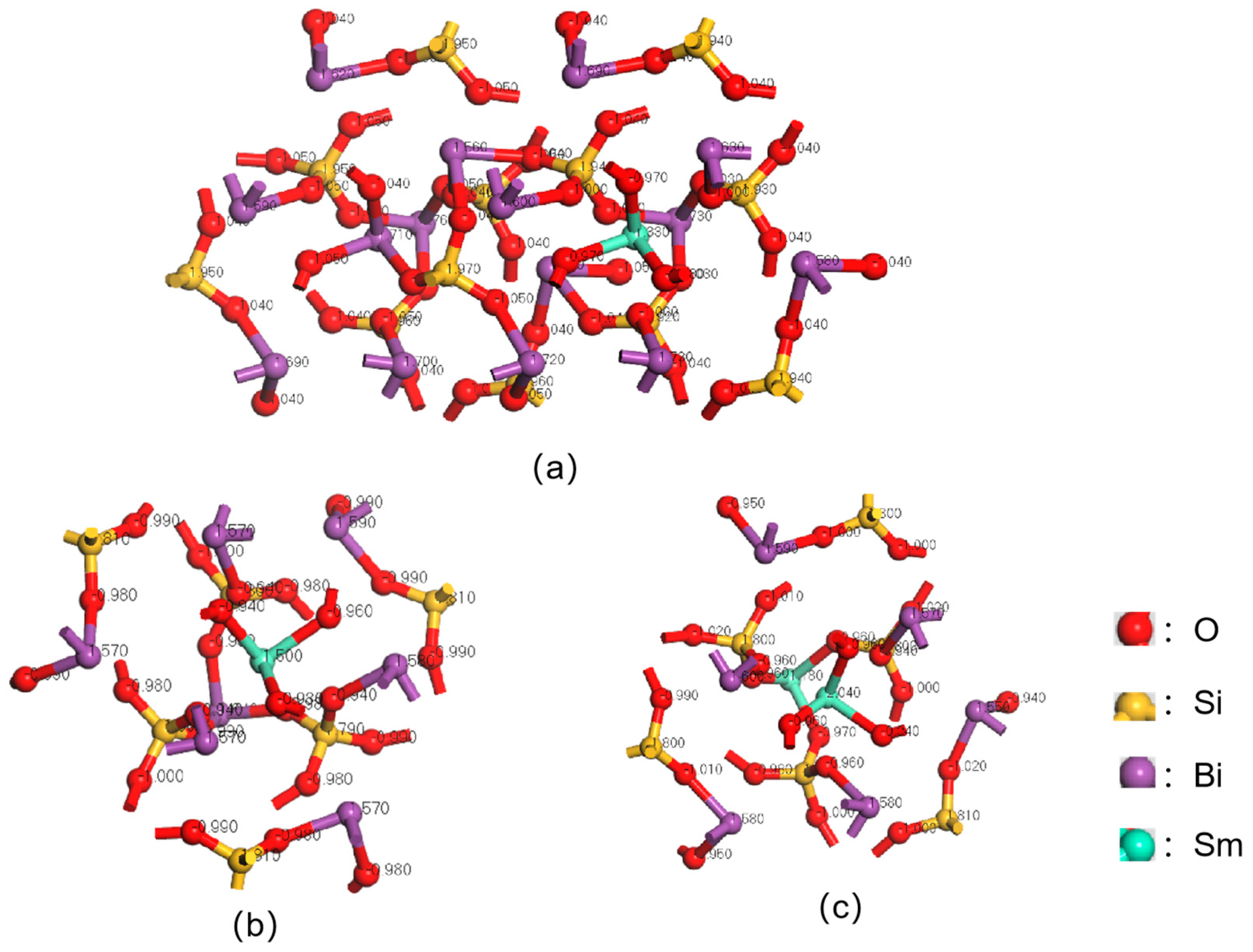
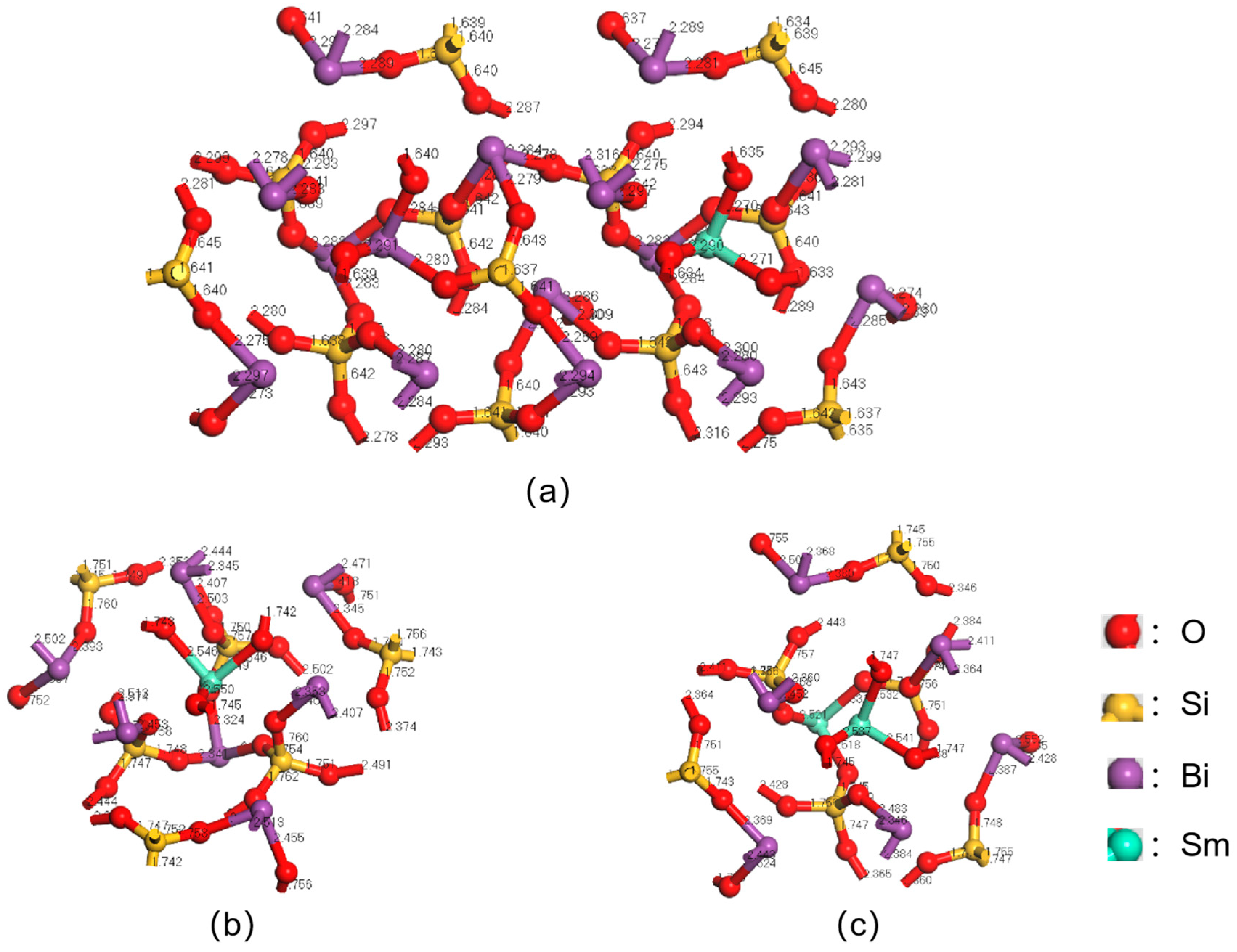
3.1. Mulliken Charge Calculation for Sm3+ Doping Level of 1/12

Upon the incorporation of Sm3+ into the BSO crystal lattice, Sm atoms substitute for Bi atoms, thereby creating the doped BSO crystal structure. The Mulliken charges corresponding to a Sm3+ doping concentration of 1/12 are presented in Table 2. From this table, it can be seen that the electron numbers of s, p, d, and f orbitals for each atom and the total number of electrons for each atom are presented. According to Table 2, the outer electron configuration of Bi atoms becomes multifaceted, and there are 15 various states in total. The average charge carried by Bi is 1.67e, with a mean valence electron configuration of Bi(6s1.846p1.50). The s orbital loses 0.16 units of electrons. The electrons in the 6p orbitals of Bi atoms are transferred to other orbitals, resulting in a loss of 1.50 units of electrons; hence, it is mainly the p orbitals that lose electrons. The average total number of electrons is 3.33 units. The average charge carried by Sm is 1.33e, with an average valence electron configuration of Sm(4f5.376s2.24). The s orbital gains 0.24 units of electrons, and the f orbital loses 0.63 units of electrons, with an average total of 14.67 units of electrons, which is 4.4 times the total number of electrons in Bi. The electronic configuration for oxygen’s outermost shell atoms extends to 14 states, with an average charge of −1.02e. The average valence electron configuration is O(2s1.872p5.15). The s orbital experiences a reduction of 0.13 electron units, while the p orbital acquires an additional 1.15 electron units, with the predominant electron accumulation occurring in the p orbital. The bonding electron structure of Si atoms is exhibited in 10 states, with an average charge of 1.95e. The average valence electron structure is Si(3s0.693p1.37), where the s orbital and p orbital lose 1.31 and 0.63 units of electrons, respectively, mainly losing electrons from the s orbital.

3.2. Mulliken Charge Calculation for Sm3+ Doping Level of 1/6

In Table 3, the Mulliken charges for a Sm3+ doping level of 1/6 are displayed. According to Table 3, there are five different states in the bonding electron configuration of Bi atoms, with a mean charge of 1.59e. The average valence electron configuration is Bi(6s1.906p1.51). The s and p orbitals lose 0.10 and 1.49 units of electrons, respectively, mainly losing electrons from the p orbital, with an average total of 3.41 units of electrons. The average charge carried by Sm is 1.50e, with an average valence electron configuration of Sm(4f5.416s2.24). The s orbital gains 0.24 units of electrons, and the f orbital loses 0.59 units of electrons, with an average total of 14.50 units of electrons, which is 4.3 times the total number of electrons in Bi. There are 12 different states in the outer electron configuration of O atoms, with an average charge of −0.97e. The mean valence electron configuration is O(2s1.892p5.08). The s and p orbitals experience a change of −0.11 and +1.08 units of electrons, respectively, mainly gaining electrons in the p orbital. There are three different states in the outer electron configuration of Si atoms, with a mean charge of 1.80e. The average valence electron configuration is Si(3s0.813p1.39). The s and p orbitals lose 1.19 and 0.61 units of electrons, respectively, mainly losing electrons from the s orbital.

3.3. Mulliken Charge Calculation for Sm3+ Doping Level of 1/3

In Table 4, the Mulliken charges for a Sm3+ doping level of 1/3 are displayed. According to Table 4, there are six different states in the outer electron configuration of Bi atoms, with a mean charge of 1.58e. The average valence electron configuration is Bi(6s1.916p1.52). The s and p orbitals lose 0.09 and 1.48 units of electrons, respectively, mainly losing electrons from the p orbital, with an average total of 3.42 units of electrons. Sm atoms have two different states in their valence electron configuration, with an average charge of 1.61e. The average valence electron configuration is Sm(4f5.256s2.22). The s and f orbitals experience a change of +0.22 and −0.75 units of electrons, respectively, with an average total of 14.39 units of electrons, which is 4.2 times the total number of electrons in Bi. There are 13 different states in the outer electron configuration of O atoms, with a mean charge of −0.98e. The average valence electron configuration is O(2s1.902p5.09). The s and p orbitals experience a change of 0.10 and 1.09 units of electrons, respectively, mainly gaining electrons in the p orbital. There are four different states in the outer electron configuration of Si atoms, with a mean charge of 1.80e. The average valence electron configuration is Si(3s0.823p1.39), where the s orbital loses 1.18 units of electrons and the p orbital loses 0.61 units of electrons, mainly losing electrons from the s orbital.

3.4. Mulliken Charge Analysis of Sm3+-Doped BSO Crystals

Figure 2 illustrates the charges of individual atoms with varying proportions of Sm3+ doping; from observing the overall structure, oxygen (O) atoms are widely distributed throughout the crystal, serving as a crucial bridge connecting other atoms. Silicon (Si) atoms tend to bond with oxygen atoms, which is an important foundation for the stability of the BSO crystal structure. Bismuth (Bi) atoms, due to their larger atomic radius and unique electronic configuration, occupy specific positions within the crystal structure, which leads to the local arrangement of atoms of Sm in the BSO crystal changing to some extent. There is a reduction charge carried by O atoms in the vicinity of Sm, which is because the radii and charge states of Sm3+ and Bi3+ are different. When Sm3+ replaces Bi3+, due to the smaller radius of Sm3+, its attraction to surrounding O atoms is stronger, causing O atoms to lose more electrons and have a relatively reduced charge. This also leads to more electrons from Bi atoms being attracted to the vicinity of Sm3+, causing a relative increase in the charge of Bi atoms near Sm. Since the doped Sm3+ replaces Bi3+ and Si is less affected by the changes in the crystal field, its charge change is not significant. With a Sm3+ doping ratio of 1/6, the outermost region of the crystalline framework includes three groups of O-Si-O-Bi-O, which are symmetric and have charge values that are very similar. Nevertheless, once the doping ratio rises to 1/3, the charge values of the three sets of O-Si-O-Bi-O in the outer layer become different from each other, losing symmetry. After doping with Sm3+, the geometric arrangement of the O-Si-O-Bi-O groups remains consistent, indicating that the crystal structure is locally symmetric. This symmetry may be reflected in the distances between atoms, the angles, and the spatial arrangement. When the doping ratio is higher, the different charge numbers lead to local distortions in the crystal structure, which disrupt the original symmetry. This distortion may be due to the different ionic radii of Sm3+ and Bi3+, causing the surrounding atoms to rearrange to accommodate the new ion, thereby affecting the local structural symmetry. This implies that a higher proportion of doping could cause the crystal structure’s symmetry to be disrupted. In Table 5, the mean charge of each atom under various Sm3+ doping ratios is shown. As the Sm3+ doping proportion increases, the total positive charge of Sm3+ increases, leading to more neutralization with the amount of negative charge on O atoms. To maintain charge balance, the Bi atoms need to neutralize fewer negative charges from O atoms, so the Bi charge relatively decreases, resulting in a decrease in conductivity. As the Sm3+ doping ratio increases, O atoms gain fewer unit electrons in their p orbitals, leading to a gradual decrease in O atom charge. Due to the doping of Sm3+, the carrier concentration in the BSO crystal is altered, thereby affecting the electrical conductivity of the crystal [20]. The reduction in charge may reduce the number of free charge carriers, thereby also reducing the material’s conductivity. Si atoms lose fewer electrons in their s and p orbitals, thus gaining more electrons. However, high doping concentrations cause the crystal structure to lose balance; this may be one of the reasons for the decreasing Si charge, while also indicating that the capacity of Si atoms to act as electron acceptors is diminishing, resulting in a decrease in the quantity of free electrons and consequently lower conductivity. Our research group [20] has also investigated the conductivity characteristics of Sm3+-doped BSO crystals, where a high concentration of impurities led to a significant decrease in carrier mobility and a reduction in conductivity. This further confirms that high doping levels result in decreased conductivity.
Figure 3 displays the bond length conditions for doping with various proportions. The variation in bond lengths within the crystal is not only adjusts the geometric structure but also carries profound chemical significance. Changes in bond lengths directly affect the chemical bond energy between atoms, which in turn influences the stability of the crystal. Due to the complexity of the crystal structure, the bonds created by the same atom exhibit slight variations depending on their quantity. Hence, we utilized the average bond length approach for our examination, as detailed in Table 6. With the increase in the Sm3+ doping proportions, the Sm-O bond length exhibited a pattern where it initially rose and subsequently fell, demonstrating the properties of a covalent bond, and was briefest when the Sm3+ doping ratio was 1/12. When the Sm3+ doping ratio was 1/6, the length of the Sm-O bond reached its highest value. This phenomenon might be because the charge number at this ratio is relatively large, which provides favorable conditions for the formation of longer bonds. Conversely, with the progressive increase in Sm3+ doping proportions, the length of the Bi-O bond increases in sequence. It attains its shortest length when the doping proportions is 1/12. Typically, the shorter the bond length, the stronger the covalent nature of the chemical bond, indicating that with a small amount of doping, that is, at a Sm3+ doping proportion of 1/12, the covalent nature of the bonds between Sm-O and Bi-O atoms is more prominent.

4. Conclusions

This study employs first-principles calculations to investigate the effects of varying concentrations of Sm3+ dopants on the crystal structure and Mulliken charge distribution in bismuth silicate. The incorporation of Sm3+ induces notable alterations in the nearby atomic arrangement in the BSO crystal lattice. The charge distribution shows a relative decrease for O atoms near Sm, an increase for Bi atoms, and minimal change for Si atoms. As the doping concentration of Sm3+ rises, reaching a proportion of 1/6, the crystal’s shell forms a symmetrical O-Si-O-Bi-O arrangement, characterized by an even distribution of charges. Nevertheless, when the doping proportion reaches 1/3, this balance is compromised. Consequently, we can conclude that high levels of doping lead to a disruption in the crystal structure’s symmetry. As the Sm3+ doping proportion increases, the charge of Bi atoms decreases because they require less neutralization of the negative charges from O atoms. The charge on O atoms decreases because they gain fewer electrons in their p orbitals. Additionally, the charge on Si atoms is reduced as a result of the structural imbalance induced by high doping levels. A high concentration of impurities leads to a significant decrease in carrier mobility, resulting in reduced conductivity. At a Sm3+ doping ratio of 1/12, both the Sm-O and Bi-O bond lengths reach their minimum values, indicating stronger covalent interactions between these atoms. This suggests that the covalent character of Sm-O and Bi-O bonds is most significant at this specific doping level. In summary, Sm3+ doping affects the charge distribution and bond lengths in the BSO crystal, thereby affecting its conductivity and the covalency of chemical bonds.

Author Contributions

Conceptualization, X.X., Y.Z. and X.Z.; data curation, Y.Z., Y.H. and J.S.; formal analysis, Y.Z.; funding acquisition, X.X., H.Z. and X.Z.; investigation, X.X., Q.X., J.S., S.L., H.Z., L.M., C.Y., T.M., J.X., T.T. and H.S.; supervision, X.X.; validation, X.X.; writing—original draft preparation, Y.Z.; writing—review and editing, Y.Z. and X.X. All authors have read and agreed to the published version of the manuscript.

Funding

This work is supported by the Ningxia Key Natural Science Foundation project (2023AAC02045), the Scientific research project of Ningxia Education Department (NYG2024067), the National Natural Science Foundation of China (61965001, 11864001, and 61461001), the Fundamental Research Funds for the Central Universities, North Minzu University (2021KJCX07), the Ningxia Province Key Research and Development Program (2018BEE03015, 2021BEE03005, and 2022BFE02009), the Natural Science Foundation of Ningxia (2019AAC03103, 2020AAC03239, and 2023AAC03304), the Ningxia first-class discipline and scientific research projects (electronic science and technology, No. NXYLXK2017A07-DKPD2023C10 and DKPD2023D01), and the Graduate Innovation Program of North Minzu University (Grant No. YCX24339).

Data Availability Statement

The original contributions presented in this study are included in the article.

Acknowledgments

The authors thank the Key Laboratory of North Minzu University (Physics and Photoelectric Information Functional Materials Sciences and Technology), the Ningxia Advanced Intelligent Perception Control Innovation Team, the Ningxia Acousto-optic Crystals Industrialization Innovation Team, and the Ningxia New Solid Electronic Materials and Devices Research and Development Innovation Team (2020CXTDLX12).

Conflicts of Interest

Author Xuefeng Zhang was employed by the company Ningxia Ju Jing Yuan Crystal Technology, Co., Ltd. The remaining authors declare that the research was conducted in the absence of any commercial or financial relationships that could be construed as a potential conflict of interest.

References

  1. Rodnyi, P.A. Physical Processes in Inorganic Scintillators; CRC Press: Boca Raton, FL, USA, 2020. [Google Scholar] [CrossRef]
  2. Akande, S.; Bouhali, O. First-principles studies of defect behaviour in bismuth germanate. Sci. Rep. 2022, 12, 15728. [Google Scholar] [CrossRef] [PubMed]
  3. Akchurin, N.; Bedeschi, F.; Cardini, A.; Cascella, M.; Ciapetti, G.; De Pedis, D.; Fasoli, M.; Ferrari, R.; Franchino, S.; Fraternali, M.; et al. A comparison of BGO and BSO crystals used in the dual-readout mode. Nucl. Instrum. Methods Phys. Res. Sect. A Accel. Spectrometers Detect. Assoc. Equip. 2011, 640, 91–98. [Google Scholar] [CrossRef]
  4. Wan, Q.; Zhang, X.; Wang, F. The elastic anisotropy electronic and optical properties of Bi4Si3O12, Bi2SiO5, Bi12SiO20 and Bi2Si3O9 crytals from first-principles calculations. Chem. Phys. Lett. 2023, 814, 140323. [Google Scholar] [CrossRef]
  5. Fischer, P.; Waldner, F. Comparison of neutron diffraction and EPR results on the cubic crystal structures of piezoelectric Bi4Y3O12 (Y = Ge, Si). Solid State Commun. 1982, 44, 657–661. [Google Scholar] [CrossRef]
  6. Xiao, X.; Xu, J.; Wei, H.; Chu, Y.; Yang, B.; Zhang, X. Optical and scintillation properties of Bi4Si3O12:RE (RE=Eu3+, Sm3+, Ho3+, Tb3+) single crystals. J. Rare Earths 2019, 37, 260–264. [Google Scholar] [CrossRef]
  7. Lira, A.C.; Martín-Rodríguez, E.; Martínez-Martínez, R.; Camarillo, I.; Muñoz, G.H.; Garcia-Solé, J.; Caldiño, U. Spectroscopy of the Bi4Si3O12: Er3+ glass for optical amplification and laser application. Opt. Mater. 2010, 32, 1266–1273. [Google Scholar] [CrossRef]
  8. Zhang, Y.; Xu, J.Y.; Zhang, T.T. Synthesis and Luminescence properties of Eu3+-droped Bi4Si3O12. J. Inorg. Mater. 2011, 26, 1341–1344. [Google Scholar] [CrossRef]
  9. Senguttuvan, N.; Kidokoro, N.; Ootsuka, K.; Ishii, M.; Kobayashi, M.; Taira, T.; Kurimura, S. Crystal growth and optical properties of Bi4Si3O12: Nd. J. Cryst. Growth 2001, 229, 188–192. [Google Scholar] [CrossRef]
  10. Lalic, M.V.; Souza, S.O. The first-principles study of electronic and optical properties of BGO and BSO scintillators. Opt. Mater. 2008, 30, 1189–1192. [Google Scholar] [CrossRef]
  11. Xiao, X.; Huang, Y.; Zhang, Y.; Si, J.; Liang, S.; Xu, Q.; Shen, H. Research on optical properties of Eu3+ doped bismuth silicate crystals based on first principles. Jpn. J. Appl. Phys. 2024, 63, 092002. [Google Scholar] [CrossRef]
  12. Guo, K.; Man, Z.Y.; Chen, H.H.; Guo, X.; Zhao, J.T. Effects of rare-earth substitution on the stability and electronic structure of REZnOSb (RE=La–Nd, Sm–Gd) investigated via first-principles calculations. Chem. Phys. 2011, 380, 54–60. [Google Scholar] [CrossRef]
  13. Yue, S.; Zhang, H. First principles study on magnetic and electronic properties with rare-earth atoms doped SWCNTs. Front. Phys. 2012, 7, 353–359. [Google Scholar] [CrossRef]
  14. Qin, Y.; Zhang, J.; Yang, H.; Fang, Z.; Fan, X.; Kuang, F.; Ye, H.; Fang, Y. Effect of uniaxial strain on electronic structure of intrinsic and N-doped 4H-SiC. Acta Phys. Chim. Sinica 2025, 42, 179–185. [Google Scholar]
  15. Zhang, Y.; Xiao, X.; Huang, Y.; Si, J.; Liang, S.; Xu, Q.; Shen, H. Eu3+-doped bismuth silicate crystal structure and Mulliken charge analysis. Cryst. Struct. Commun. 2024, 80, 815–820. [Google Scholar] [CrossRef] [PubMed]
  16. Nordheim, L. Zur elektronentheorie der metalle. I. Ann. Der Phys. 1931, 401, 607–640. [Google Scholar] [CrossRef]
  17. Brik, M. First-principles calculations of electronic, optical and elastic properties of ZnAl2S4 and ZnGa2O4. J. Phys. Chem. Solids 2010, 71, 1435–1442. [Google Scholar] [CrossRef]
  18. Liu, B.X.; Lai, W.S.; Zhang, Z.J. Solid-state crystal-to-amorphous transition in metal-metal multilayers and its thermodynamic and atomistic modelling. Adv. Phys. 2001, 50, 367–429. [Google Scholar] [CrossRef]
  19. Mulliken, R. Electronic population analysis on LCAO-MO molecular wave functions. I. J. Chem. Phys. 1955, 23, 1833–1840. [Google Scholar] [CrossRef]
  20. Huang, Y.; Xiao, X.; Zhang, Y.; Si, J.; Liang, S.; Xu, Q.; Shen, H. Study on the Optical Properties of Sm3+ Doped Bismuth Silicate Crystals Based on First Principles. Mater. Res. Express 2024, 11, 115902. [Google Scholar] [CrossRef]
Figure 1. BSO crystal structure with Sm3+ doping concentrations of 1/12 (a), 1/6 (b), and 1/3 (c).
Crystals 15 00423 g001
Figure 2. Charge structure of BSO crystals doped with Sm3+ at concentrations of 1/12 (a), 1/6 (b), and 1/3 (c).
Crystals 15 00423 g002
Figure 3. Bond length structures of BSO crystals doped with Sm3+ at concentrations of 1/12 (a), 1/6 (b), and 1/3 (c).
Crystals 15 00423 g003
Table 1. The variation in cell parameters with different doping proportions.
ProportionChemical Formulaa/Åb/Åc/Å α β γ
1/12Bi15SmSi12O4817.8857348.9373198.940963109.47279109.54748109.54261
1/6Bi7SmSi6O249.78119.79029.7937109.3735109.5783109.4024
1/3Bi6Sm2Si6O249.77639.7589.7597108.8562108.9487108.9563
Table 2. Mulliken charges for Sm3+ doped at 1/12 concentration.
Atom spdfTotalCharge/e
O11.875.177.05−1.05
O21.875.167.04−1.04
O31.875.177.04−1.04
O41.885.177.05−1.05
O51.885.177.04−1.04
O61.875.187.05−1.05
O71.885.157.03−1.03
O81.885.167.04−1.04
O91.875.167.03−1.03
O101.865.116.87−0.97
O111.865.147.00−1.00
O121.865.126.97−0.97
O131.865.137.00−1.00
O141.865.126.98−0.98
Si10.691.352.041.96
Si20.691.362.041.96
Si30.681.362.051.95
Si40.691.372.051.95
Si50.701.372.071.93
Si60.701.362.061.94
Si70.691.372.061.94
Si80.691.362.061.94
Si90.701.372.081.92
Si100.681.352.031.97
Sm2.246.031.045.3714.671.33
Bi11.891.503.381.62
Bi21.741.503.241.76
Bi31.801.513.311.69
Bi41.931.503.421.58
Bi51.911.503.411.57
Bi61.791.503.291.71
Bi71.951.503.441.56
Bi81.801.503.301.70
Bi91.821.503.311.69
Bi101.771.503.271.73
Bi111.781.493.281.72
Bi121.821.493.311.69
Bi131.901.503.401.60
Bi141.871.513.371.63
Bi151.761.513.271.73
Table 3. Mulliken charges for Sm3+ doped at 1/6 concentration.
Atom spdfTotalCharge/e
O11.895.106.99−0.99
O21.905.076.98−0.98
O31.905.096.99−0.99
O41.905.086.98−0.98
O51.895.096.98−0.98
O61.895.066.96−0.96
O71.895.056.94−0.94
O81.895.046.93−0.93
O91.905.107.00−1.00
O101.895.046.94−0.94
O111.895.096.99−0.99
O121.905.117.00−1.00
Si10.811.392.201.80
Si20.801.392.191.81
Si30.821.392.211.79
Sm2.246.020.835.4114.501.50
Bi11.921.513.431.57
Bi21.851.513.361.64
Bi31.911.503.411.59
Bi41.901.523.421.58
Bi51.911.533.431.57
Table 4. Mulliken charges for Sm3+ doped at 1/3 concentration.
Atom spdfTotalCharge/e
O11.895.086.97−0.97
O21.895.066.95−0.95
O31.905.076.98−0.98
O41.895.127.01−1.01
O51.895.076.96−0.96
O61.895.056.95−0.95
O71.905.117.00−1.00
O81.905.127.02−1.02
O91.895.056.94−0.94
O101.905.107.01−1.01
O111.895.066.96−0.96
O121.905.137.02−1.02
O131.905.096.99−0.99
Si10.821.382.201.80
Si20.821.392.211.79
Si30.811.392.201.80
Si40.811.382.191.81
Sm12.226.110.815.6714.821.18
Sm22.226.110.804.8213.962.04
Bi11.901.513.411.59
Bi21.911.513.421.58
Bi31.921.533.451.55
Bi41.891.513.401.60
Bi51.911.523.431.57
Bi61.901.523.421.58
Table 5. Average charges per atom in the case of various ratios Sm3+ doping concentrations.
ProportionAtomAverage Charge/e
1/12O−1.02
Si1.95
Bi1.67
Sm1.33
1/6O−0.97
Si1.80
Bi1.59
Sm1.50
1/3O−0.98
Si1.80
Bi1.58
Sm1.61
Table 6. Average bond lengths for various proportions of Sm3+ doping.
ProportionBondLength/Å
1/12Sm-O2.28
Bi1-O2.29
Bi2-O2.29
Bi3-O2.29
Bi4-O2.28
Bi5-O2.28
Bi6-O2.29
Bi7-O2.28
Bi8-O2.28
Bi9-O2.28
Bi10-O2.29
Bi11-O2.29
Bi12-O2.28
Bi13-O2.30
Bi14-O2.30
Bi15-O2.29
1/6Sm-O2.55
Bi1-O2.43
Bi2-O2.34
Bi3-O2.41
Bi4-O2.39
Bi5-O2.43
1/3Sm1-O2.52
Sm2-O2.54
Bi1-O2.42
Bi2-O2.45
Bi3-O2.46
Bi4-O2.39
Bi5-O2.43
Bi6-O2.40
Disclaimer/Publisher’s Note: The statements, opinions and data contained in all publications are solely those of the individual author(s) and contributor(s) and not of MDPI and/or the editor(s). MDPI and/or the editor(s) disclaim responsibility for any injury to people or property resulting from any ideas, methods, instructions or products referred to in the content.

