1. Introduction
Gallium selenide (GaSe) is an important member of layered post-transition metal chalcogenides, which are suitable for the formation of van der Waals heterointerfaces [
1] and fabricating various quasi-two-dimensional structures [
2,
3,
4,
5,
6], with high potential for application in electronic and optoelectronic devices. The interlayer binding energy of GaSe is calculated to be in the range of 14–16 meV/Å
2 [
7]. The layered nature has the possibility of producing ultrathin sheets through exfoliation, as well as of introducing impurity atoms into the interlayer space (intercalation) for the preparation of structures with new properties [
8,
9]. The main application of GaSe crystals is in nonlinear optics as a medium for converting the frequency of laser radiation into the IR and terahertz frequency ranges [
10,
11]. Currently, it is one of the promising materials for obtaining a high repetition rate IR and THz optical parametric oscillators/amplifiers (OPOs/OPAs) [
12] and high peak power laser beam frequency conversion to achieve GW-level (multi)terahertz pulses [
11].
One of the areas of research concerning GaSe is the study of the properties of nanolayered A
3B
6 compounds, methods for their preparation, and applications in photodetectors [
4,
13] and gas sensors [
3,
14]. It is established that nanolayered materials with a small area of the working surface often significantly change their properties, primarily conductivity, under the influence of optical radiation [
3,
13]. This leads to high values of photosensitivity. For example, in GaS, this is associated, among other things, with an increase in mobility and absorption coefficients due to modification of the electronic structure during the transition from bulk to nanosized form [
4]. Thus, the final parameters may depend on the method of obtaining the structures, the presence of defects and chemical impurities, and the thickness of the layers. In particular, the presence of mechanical strains, for example, when the semiconductor layers are deformed on a flexible substrate [
15], can have a significant effect on the performance characteristics.
According to the available data, GaS and GaSe compounds possess the highest photosensitivity values among other representatives of the A
3B
6 family [
3,
4]. It is also known that high-energy particle bombardment can be used to modify the electrical and optical properties of semiconductors [
16,
17]. In particular, this can be employed to obtain modified 2D structures, either specially grown or cleaved from the irradiated bulk materials. At present, the physical properties of GaSe under the influence of high-energy particles have not been sufficiently studied. Recently, the optical and dielectric characteristics of GaSe crystals modified by irradiation with high-energy electrons were analyzed [
18]. The appearance of “steps” in the optical transmission spectra was reported. It should be pointed out that (i) similar “steps” were previously observed for neutron-irradiated GaS [
17], and (ii) the arising radiation defect absorption can increase the spectral range of photosensitivity of bulk and nanolayered A
3B
6 photodetectors. The investigation of the defect energy levels in irradiated semiconductors can be accomplished using the deep level transient spectroscopy (DLTS) technique [
19,
20]. DLTS, in combination with the measurements of current-voltage and capacitance-voltage dependencies, is known to be a powerful tool to determine the concentration of defects and their activation energies.
In the present paper, the results of the study of electron-irradiated GaSe samples by DLTS method are reported. First, we analyze the optical absorption spectra measured at various temperatures to obtain the temperature-dependent optical transition energies. Then, we employ DLTS together with I–V and C–V measurements to obtain electrical characteristics of the defects: activation energies, concentrations, and hole capture cross-sections.
3. Results and Discussion
In our previous research, it was found that two bands appear in the optical absorption spectra of GaSe crystals after irradiation with 9 MeV electrons [
18]. These absorption bands were associated with gallium vacancies in two charge states,
and
, inducing levels with energy positions in the forbidden gap of the crystal, respectively,
Ev + 0.23 eV and
Ev + 0.61 eV at
T = 295 K, where
Ev is the valence band maximum (VBM).
It should be noted that a defect state with an energy level about
Ev + 0.2 eV was found in a number of Hall effect, DLTS, thermally stimulated current (TSC), and photoluminescence studies of GaSe crystals and usually attributed to a gallium vacancy (for example, [
25,
26,
27,
28]). This conclusion finds support in the results of first principles DFT calculations [
29,
30]. The computer simulation of point defects in the β-polytype of GaSe in ref. [
29] with large (up to 400 atoms) supercells and using semilocal density functional revealed the presence of an energy level
Ev + 0.26 eV, generated by the gallium vacancy. The corresponding defect state has a moderately deep character and splits off the valence band. An unoccupied gap state with an energy level
Ev + 0.92 eV at the Г point was also obtained in ref. [
29] for GaSe with a Ga vacancy. In recent theoretical studies of electronic and structural properties of GaSe with intrinsic defects [
30], an optimized HSE functional allowing better reproducing excited states was employed. The (0/−) charge transition level for a Ga vacancy was calculated to be
Ev + 0.1 eV. Note that the authors of ref. [
30] did not find the (−/−2) charge transition level for V
Ga with the Fermi level lying within the band gap. In an even more recent paper [
31], devoted solely to monolayers of GaSe, some results of ref. [
30] were disputed and, at least for the monolayer GaSe, the gallium vacancy was related to deep states.
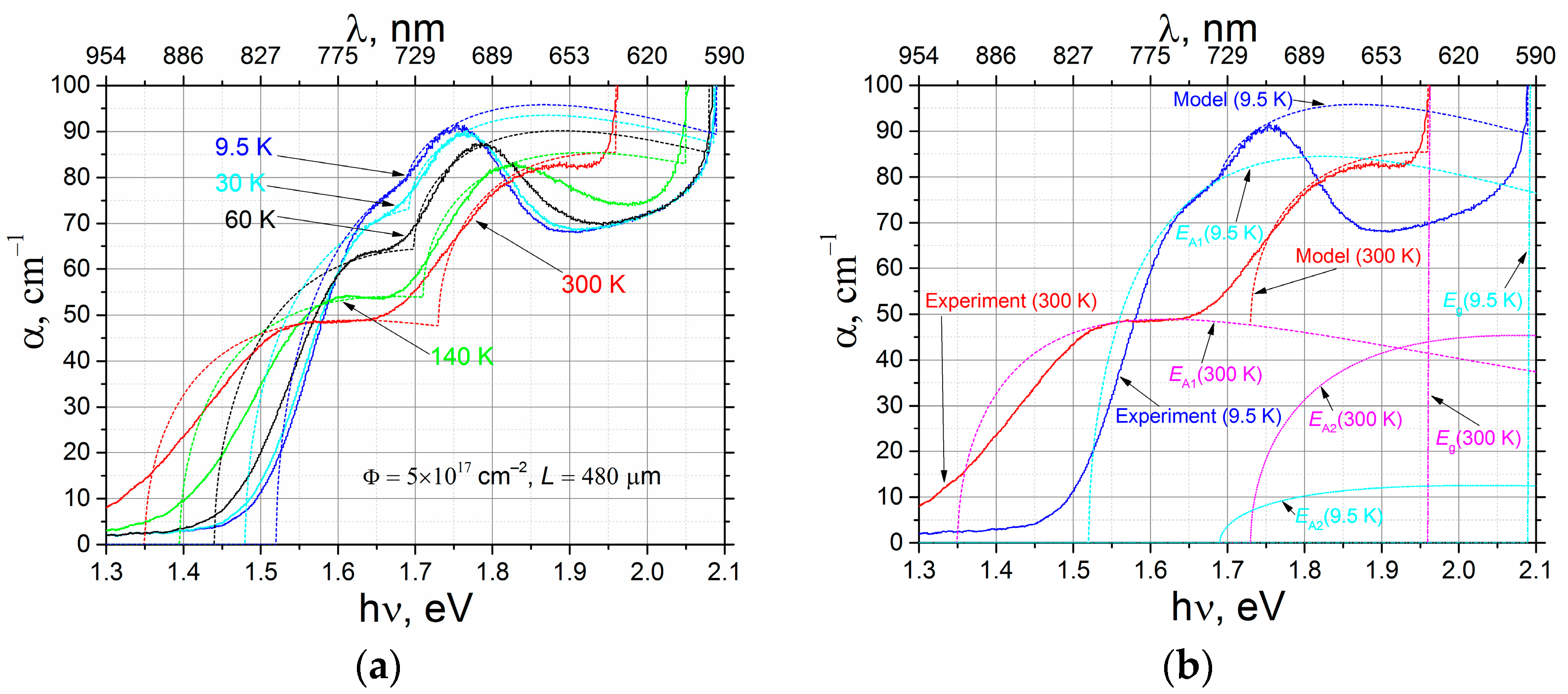
In the present work, we have performed fittings with Equation (1) for all the measured absorption spectra for a GaSe sample irradiated with a fluence of 5 × 10
17 cm
−2. The obtained data are presented in
Figure 1. First, the examples of fitting curves for the spectra measured at 9.5, 30, 60, 140, and 300 K are shown in
Figure 1a; the data for only five temperature points are chosen for simplicity. In order to better illustrate the contribution to the resulting absorption spectra of each of the defect states, the model curves resolved into contributions from each of three terms in Equation (1) are provided in
Figure 1b for the spectra at temperatures of 9.5 and 300 K.
It can be seen that the model for Equation (1) provides a satisfactory description of the observed spectral features (
Figure 1). The main discrepancy is between the experimental and the model curves in the spectral range of 1.8–2.09 eV for T = 9.5 K. Using the dispersion relation n
o(λ) [
24] when calculating the absorption coefficients α(λ) from the measured transmission spectra T(λ) can be among the possible reasons. This dispersion relation is determined for room temperature conditions and therefore may deviate from real dispersion of the refractive index at low temperatures, especially in the range above 1.8 eV, close to the room temperature band gap of GaSe. The main source of the discrepancy is the inherent limitation of the Lucovsky model, where δ function-like potential is taken for the localized deep state [
21,
22]. If a non-zero radius of the localized potential were introduced into the model, the high-photon-energy tail after the absorption maximum would become shorter, and this would better match the spectral features observed in
Figure 1. Also, the energy interval between the optical transition threshold
EA2 and the fundamental absorption edge becomes larger at lower temperatures, and a dip in the experimental spectrum is observable.
In the present work, we index the defect activation energies (charge transition levels) Δ
Eaj and threshold energies for optical transitions
EAj in ascending values. Thus, for
, the associated defect is Δ
Ea1 =
EA2 −
Eg, while, for
, the associated defect is Δ
Ea2 =
EA1 −
Eg. The physical sense of these quantities is also clear from
Figure 2a.
The obtained temperature-dependent optical transition energies
EA1 and
EA2 and related defect activation energies Δ
Ea1 and Δ
Ea2 are displayed in
Figure 2b. It is seen that the
induced energy level has a tendency to move closer to the VBM with the increasing temperature (shifts downward by 0.17 eV when the temperature changes from 9.5 to 300 K), while the
associated energy level shifts slightly upward.
From a theoretical point of view, the prediction and interpretation of temperature-driven changes in the defect level position is a complex problem. In ref. [
32], a theoretical approach to assessing the temperature shift of the charge transition level was developed, in which the main role was played by changes in the local volume around the defect and band edge positions. According to the rules formulated in ref. [
32], and taking into account the observed Δ
Ea1 and Δ
Ea2 temperature dependencies (
Figure 2b), the charge transition −/−2 induces a small change in the local volume, while this change is larger for the transition 0/−1, which leads to level shifts in opposite directions. Note that a large lattice reconstruction around the V
Ga defect is predicted in refs. [
29,
31]. It can be supposed that, at further ionization, the lattice reconstruction will not be that large. Here, we also assume that GaSe is a semiconductor in which VBM rises with temperature (type I semiconductor [
32]). This is partly supported by the results of our studies of the influence of hydrostatic pressure on the interatomic distances and interband transitions in GaSe [
7,
33]. Qualitatively, the contraction of the crystal lattice with decreasing the temperature can be compared with that after the application of pressure. The contraction of the interlayer space increases the overlapping of Se
pz orbitals, which form the highest valence band and therefore pushes the VBM up in energy.
The temperature-dependent concentrations of the optically active defects calculated using the found values of fitting parameters
A1 and
A2 and Equation (2) are given in
Figure 2c. It is seen that, with the increasing temperature, the concentration of
defects is reduced, while the concentration of
is increased. At temperatures above 225 K, the majority of the optically active Ga vacancy defects are expected to be in a −2 charge state. The found temperature dependence of the GaSe band gap,
Eg, is shown in
Figure 2d. The experimental data were fitted by the Varshni formula [
34]:
where
Eg(0) is the band gap value at
T = 0 K, and β and γ are constants. The found fitting parameters are given in
Figure 2d. The obtained
Eg(0) value is close to the one reported in ref. [
35].
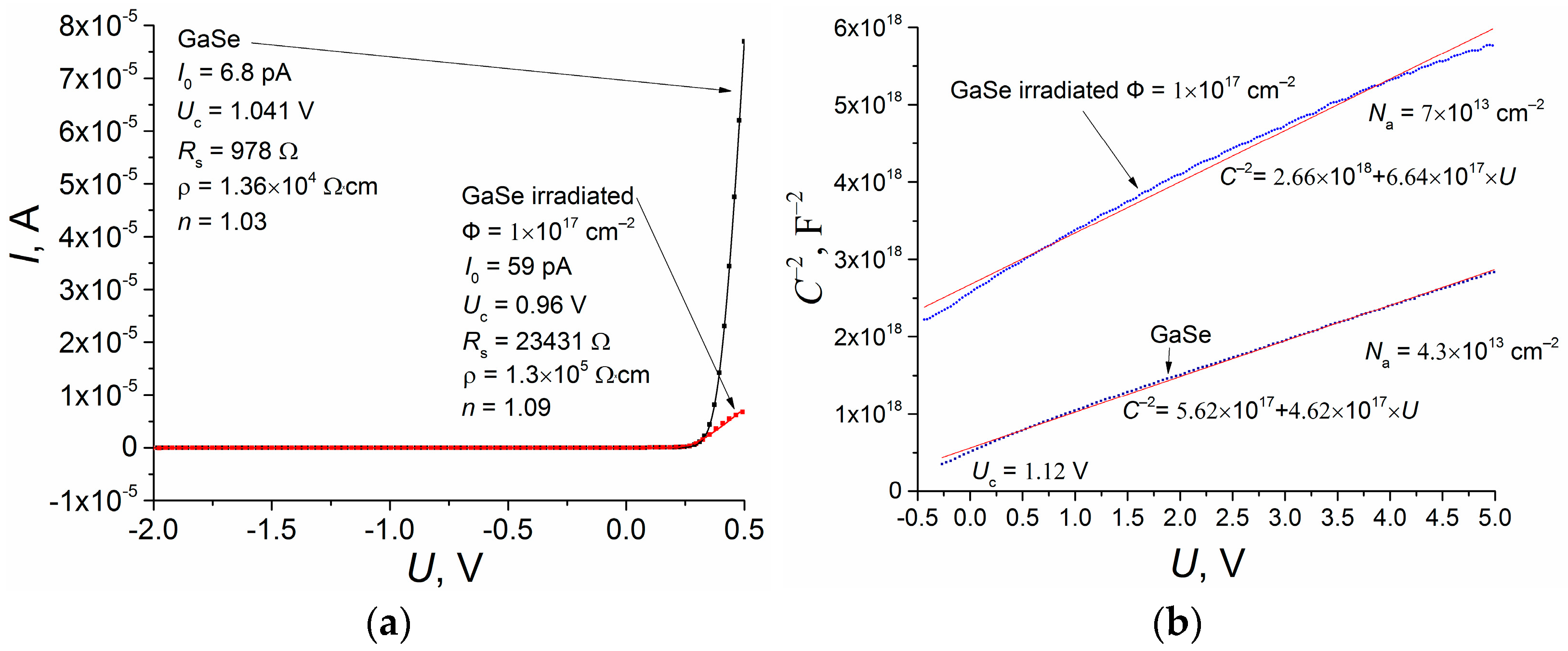
As is known, I–V characteristics of a Schottky diode can carry information about the barrier height and the series resistance of the sample, Rs. The latter parameter is important for determining the measurement mode using DLTS. In the case of large Rs values, measurements may become impossible or require compensation for the high bulk resistance of the sample when processing the measurement data.
In this work, the experimentally obtained
I–
V characteristics of the Sc/GaSe Schottky barrier (
Figure 3a) were approximated by the well-known equation (for example, [
36])
where
is the voltage at the metal-semiconductor junction,
U is the applied external voltage,
e is the electron charge,
k is the Boltzmann constant,
T is the sample temperature,
n is the ideality factor, and
I is the current flowing through the sample. The saturation current
I0 is described by the expression
where
S is the contact area, φ
b is the Schottky barrier height, and
is the effective Richardson constant, and
h is Planck’s constant. The effective mass for holes in GaSe
m* = 0.5
m0 was assumed [
37], where
m0 is the free electron mass.
The energy barriers for electrons
and holes
are estimated using the charge neutrality level concept (CNL) as [
38]
Here, the energy position of the charge neutrality level
CNLabs = (
Eg −
CNLv +
EA) is determined relative to the vacuum level. The parameter
S is calculated according to the expression
which takes into account the screening of the interface dipole induced by the metal in the semiconductor. In Equation (9),
= (
×
)
1/2. For ε-GaSe,
= 6.55, which gives S ≈ 0.25. The other physical parameters used to estimate the barrier heights
and
on the metal/GaSe(0001) interfaces are the band gap
Eg = 2 eV at
T = 300 K, the electron affinity
EA = 3.6 eV, and the charge neutrality level position with respect to the VBM: CNL
v =
Ev + 0.83 eV (
CNLabs = 4.77 eV) [
38]. According to the calculations using Equation (8), the barrier height for holes at the Sc/GaSe interface constitutes 1.12 eV, assuming the work function Φ
m = 3.5 eV for Sc. For the Pt/GaSe interface (the Pt work function is Φ
m = 5.65 eV),
= 0.6 eV.
The measured
I–
V characteristics and the results of the fittings by Equations (4)–(7) are shown in
Figure 3a. It can be noted that the obtained data for the barrier height at the Sc/GaSe interface are in good agreement with the calculation result using Equation (8), especially for the case of the unirradiated sample. It can also be noted that the electrical resistance of the sample,
Rs, increased after electron irradiation. This agrees with the CNL position calculated in ref. [
38], since, at irradiation, the Fermi level moves towards CNL, and as in the unirradiated GaSe crystals, it is usually located at 0.1–0.3 eV above the VBM, and the acceptor compensation increases.
The measured
C–
V characteristics of the GaSe samples under study are presented in
Figure 2b. In the case of a Schottky barrier, the
C–
V curves are described by the equation [
36]
where
Na is the acceptor concentration, ε
0 is vacuum permittivity, ε is the low-frequency relative permittivity of the crystal,
Uc is the contact potential difference,
U is the applied voltage, and
C is the Schottky barrier capacitance.
Figure 3b shows the fittings to the experimental data by Equation (10).
As in the case of the
I–
V characteristics, good agreement can be noted between the Schottky barrier height determined from Equation (8) and that found from the experimental data fitting by Equation (10) (for the Sc/as-grown GaSe interface). At the same time, the calculated acceptor concentrations in the irradiated sample are much lower than the corresponding values obtained from the optical data (cf. the
N values in
Figure 2c and
Figure 3b). Partly, this can be explained by the lower electron fluence 1 × 10
17 cm
−2 for the sample used in electrical measurements and by an unintentional annealing of defects during a contact deposition at a temperature about 300 °C, but the predominant reason is probably due to the inherent differences and limitations of the optical and electrical techniques used, as well as of the employed models. Nevertheless, the obtained
Na values were further used, as is usually done, to estimate the defect concentrations responsible for the appearance of DLTS peaks.
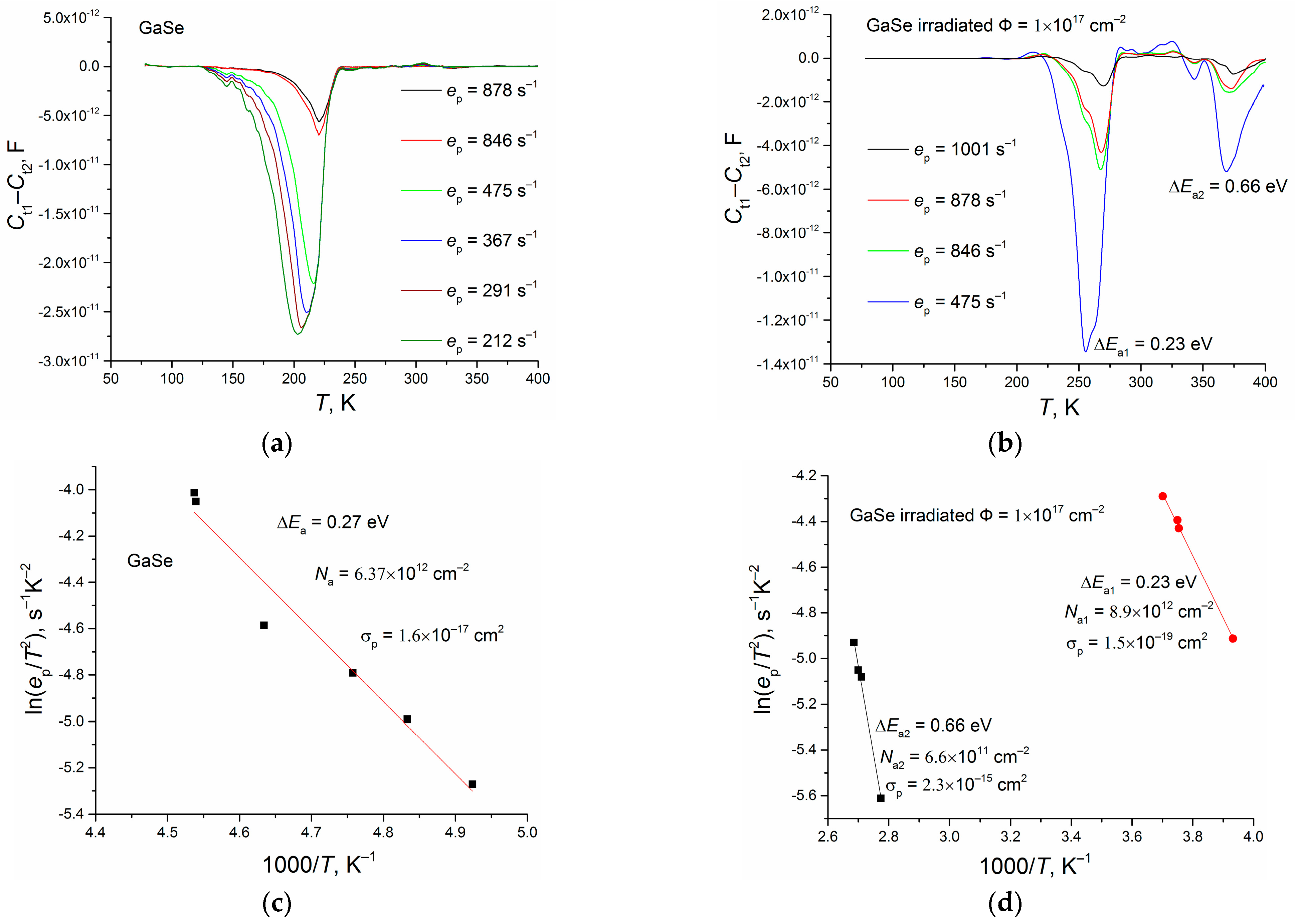
DLTS is a commonly used technique for determining the electrical parameters of defects in semiconductors. Therefore, it is reasonable to compare the results of a study using optical absorption spectroscopy with DLTS data. Standard DLTS analysis is based on registering capacitance transients after the end of the filling voltage pulse, and the emission rate changes with the temperature (determining the emission rates at a number of temperatures allows to obtain an Arrhenius plot like in
Figure 4). This allows determining the defect energy level with respect to the conduction or valence band. It is clear that the Arrhenius plot shows the Δ
Ea position, which is assumed to be temperature-independent [
19,
20]. Like any experimental method, DLTS has its limitations. It is known that it, for example, hardly resolves closely lying energy levels with close emission rates. Laplace DLTS analysis can help in this case [
20]. Maybe a set of capacitance transients measured in a narrow temperature range would allow to relate the corresponding Δ
Ea value to a distinct temperature. More reliable interpretation of DLTS activation energies requires first principles calculations to reveal the possible contribution from lattice reconstruction and surmounting of temperature-dependent capture barriers [
39].
The time constants τ, as is known [
19,
20], are inversely proportional to the emission rate of the charge carriers (holes):
where
t1 and
t2 are time delays from the back edge of the filling pulse (
t1 <
t2).
The obtained DLTS spectra are shown in
Figure 4a,b. It is possible to note the presence of a broad peak in the temperature range of 200–220 K for the unirradiated GaSe. In the DLTS spectra of the GaSe crystal irradiated with high-energy electrons, this peak shifts toward higher temperatures and becomes distorted. At the same time, a peak of lower intensity is observed at a temperature of about 370 K, which is clearly not visible in the spectra of the unirradiated crystal.
When processing the data following the conventional procedure [
19,
20,
37], it was assumed that
where ν
p is the thermal velocity of holes (~
T1/2), σ
p is the hole capture cross-section,
Nv is the effective density of the states for the top of the valence band (~
T3/2), and Δ
E is the activation energy of the trap. The defect concentrations were estimated as [
19,
20,
37]
where Δ
C is the difference in the structure capacitance at the beginning and the end of the capacitance transient, and
C0 is the structure capacitance during the filling pulse. The results of the DLTS data processing are presented in
Figure 4c,d. For the irradiated GaSe sample, the obtained defect activation energies are in good agreement with the energy positions of the levels deduced from the optical transmission measurements at 300 K (
Figure 1b and ref. [
18]). The physical meaning of the determined defect-associated “energy positions” is, in the case of DLTS, closely related to the charge transition levels, while the optical transition energies are more directly related to the energy intervals between the levels in the forbidden gap. Nevertheless, our measurement values are close.
It should be noted that the DLTS spectra obtained differed from those reported earlier in other studies. The most similar results were obtained in ref. [
25] at photoexcitation of the sample. The spectrum registered in ref. [
25] for a specially undoped GaSe sample contained two peaks, corresponding to the defect levels at
Ev + 0.2 eV and
Ev + 0.8 eV. This resembles the spectrum obtained in our work for the electron-irradiated crystal. At the same time, in ref. [
28], using a similar technique, five peaks were found for high-resistivity GaSe samples. The DLTS spectra for GaSe:Cd crystals demonstrated in ref. [
37] contained a single broad peak in the temperature range of 250–270 K, which was similar to the data presented in
Figure 4a. This peak was attributed by the authors to the presence of defects including a Cd impurity, but its origin could also be connected with the formation of intrinsic lattice defects as a result of the introduction of cadmium atoms. Finally, four well-resolved DLTS peaks were observed for a GaSe:In sample in the temperature range from 100 to 350 K in ref. [
27]; the defect level with the energy position
Ev + 0.22 eV was associated with the presence of a Ga vacancy, while the defect level at
Ev + 0.44 eV was attributed to a complex of V
Ga and an indium impurity atom.
A detailed analysis of the possible nature and differences of DLTS peaks in various GaSe samples was provided in ref. [
28], where a peak related to Ga vacancy appeared at 0.17 eV above the VBM. The same peak was observed in ref. [
25]. An additional peak at 100–115 K was recorded at 0.13 eV below the conduction band minimum. The used method (with photoexcitation) did not allow distinguishing between traps for electrons and holes, but the author supposed that this was a trap for minority charge carriers (electrons). Here, it is important to note that a similar peak was seen in our samples when the filling pulse changed the sign of the total applied voltage (its amplitude was higher than that of the reverse bias pulse). On the other hand, the amplitude of this peak was small, and its maximum did not show clear rate window dependence. Therefore, this data were not analyzed in the present paper. In ref. [
28], was is also stated that the defect level at 0.53 eV was related to defect complexes of V
Ga-metal impurity atoms, justifying this by the fact that close values were found in metal-doped GaSe crystals [
27,
37,
40,
41]. It is also mentioned in ref. [
25] that this peak was not detected, which was explained by a higher resistivity of the sample (less amount of uncontrolled impurity elements). In ref. [
28], the defect level at energy of 0.75 eV, which was close to 0.68 eV found in the present study, was associated with extended defects, like dislocations or stacking faults. It was justified by high values of captured cross-sections.
Thus, it can be concluded that the origin of crystals and post-growth treatment have a strong impact on their defect structure (registered DLTS spectra). It can be also pointed out that a similar picture of the DLTS peaks related to the divacancies in two charge states was previously observed in high-energy particle irradiated Si [
42].


 ,
, 