
High-Performance Ferroelectric Capacitors Based on Pt/BaTiO3/SrRuO3/SrTiO3 Heterostructures for Nonvolatile Memory Applications


Abstract

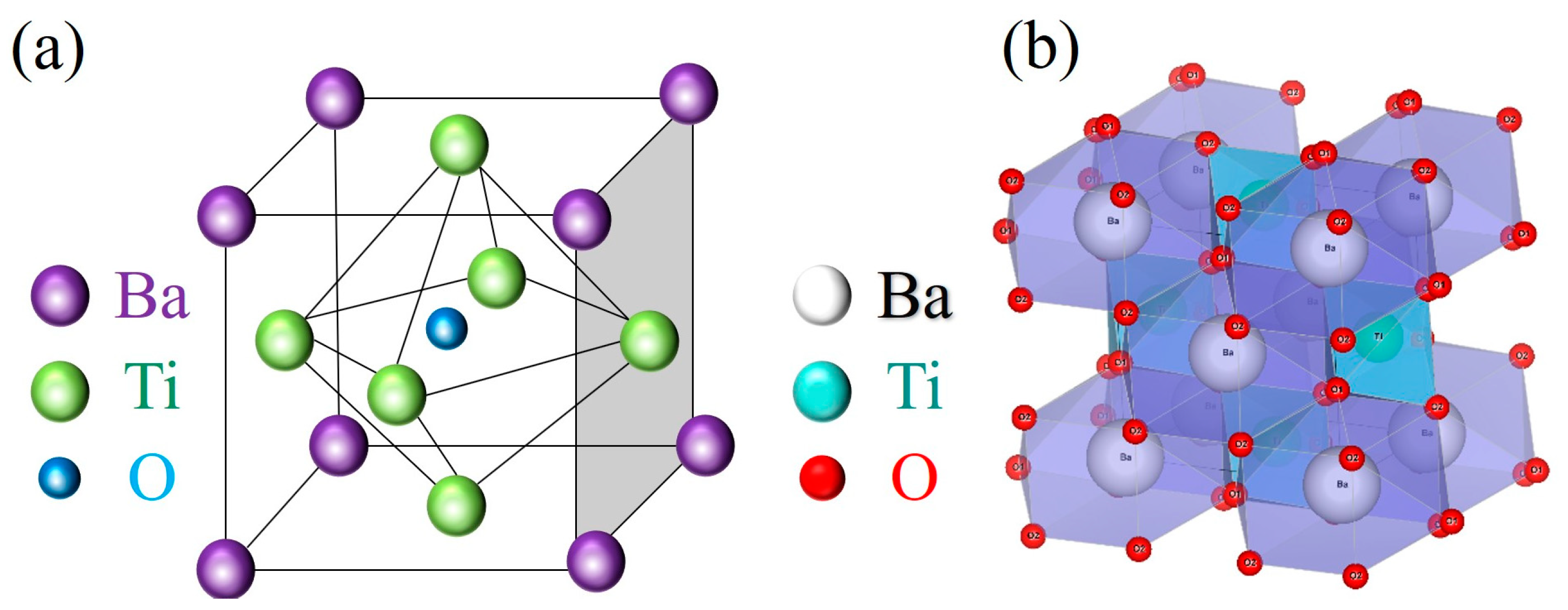
1. Introduction
2. Materials and Methods
2.1. Experimental Section and Materials
2.1.1. Epitaxial Growth
2.1.2. UV Lithography
2.1.3. Magnetron Sputtering
2.1.4. Materials
2.2. Test Methods
3. Results
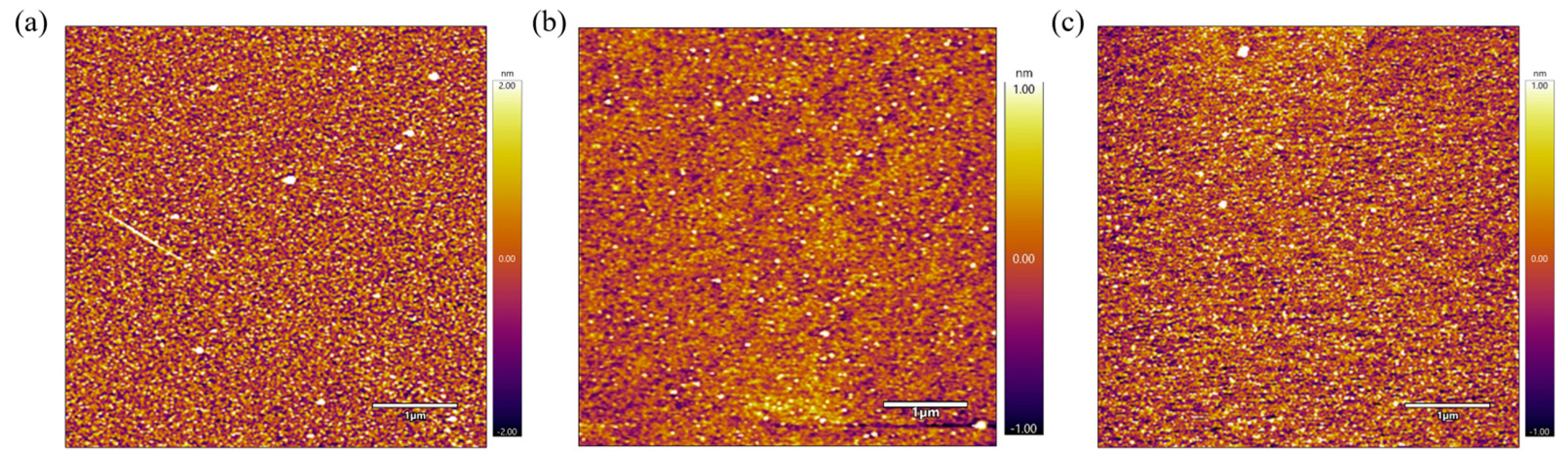
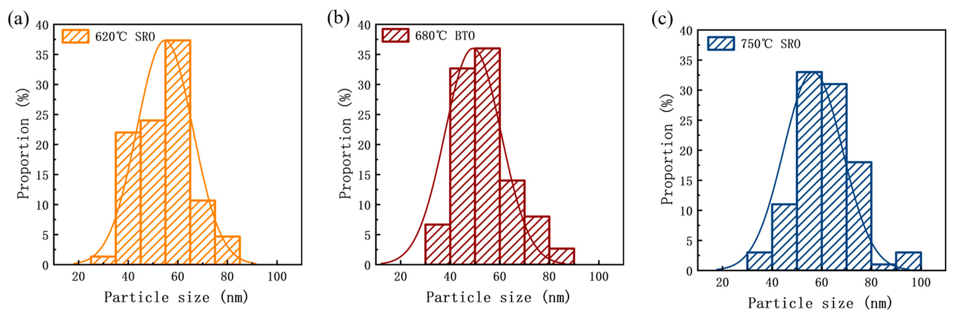
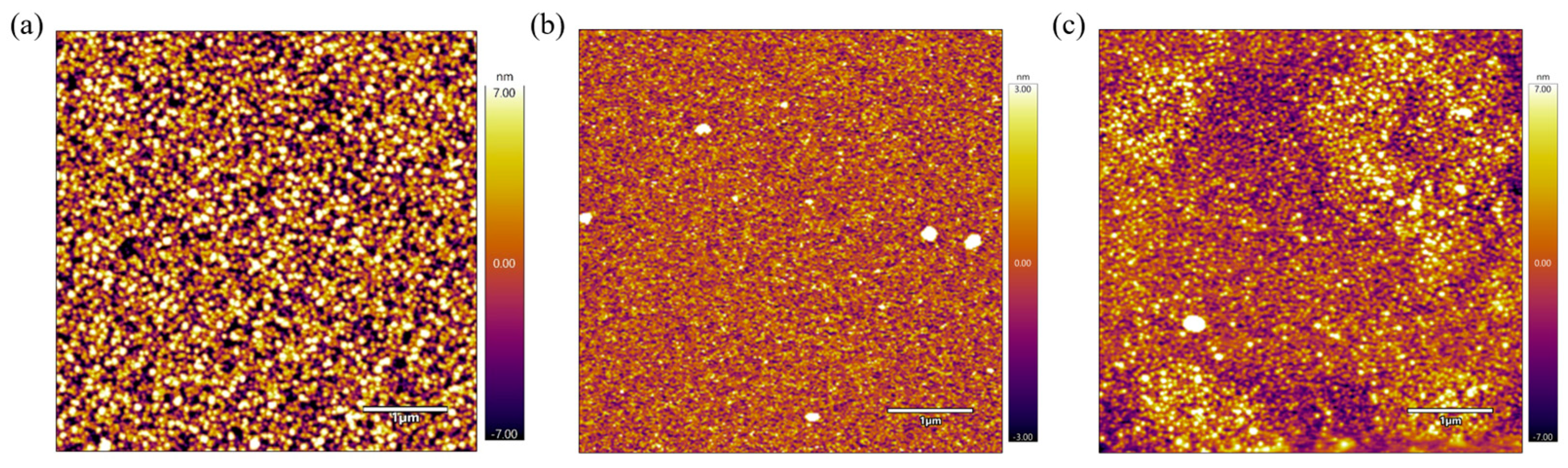
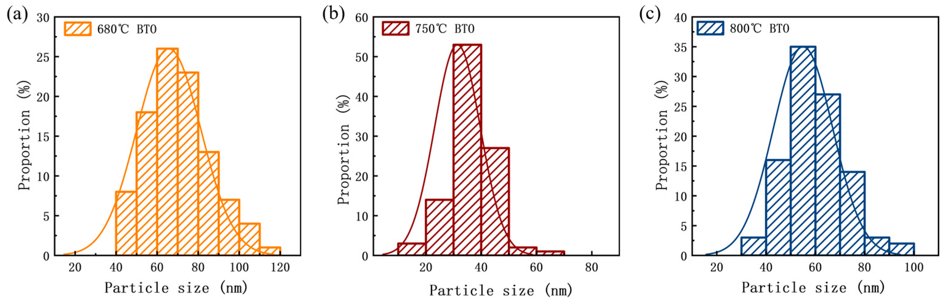
3.1. Scanning Probe Microscopy Analysis
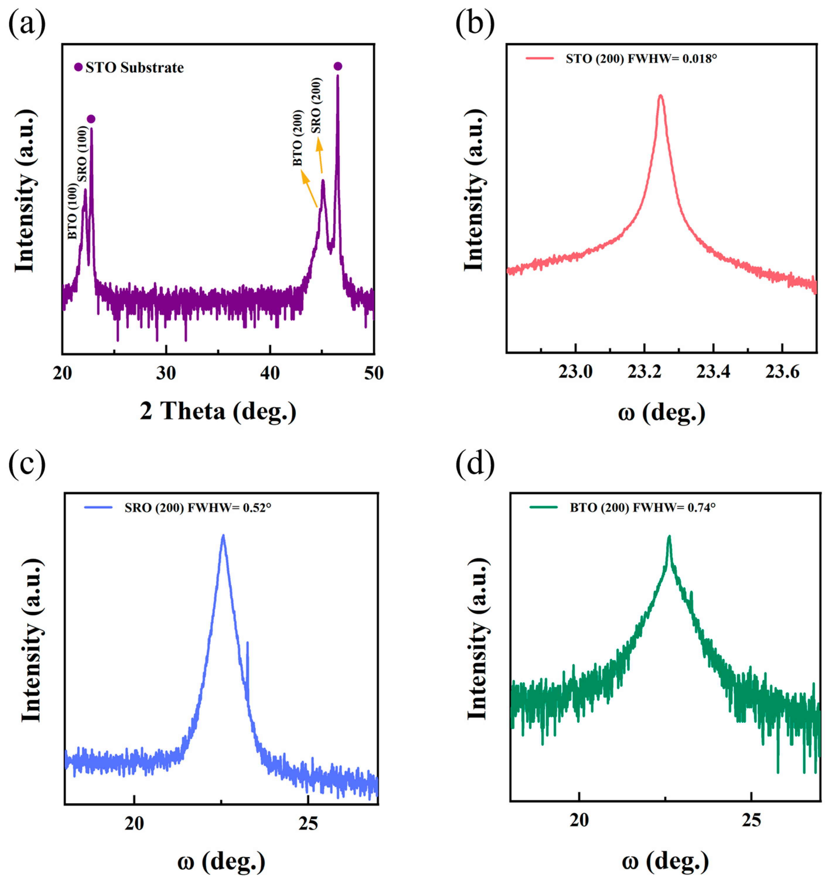
3.2. X-Ray Diffraction Analysis
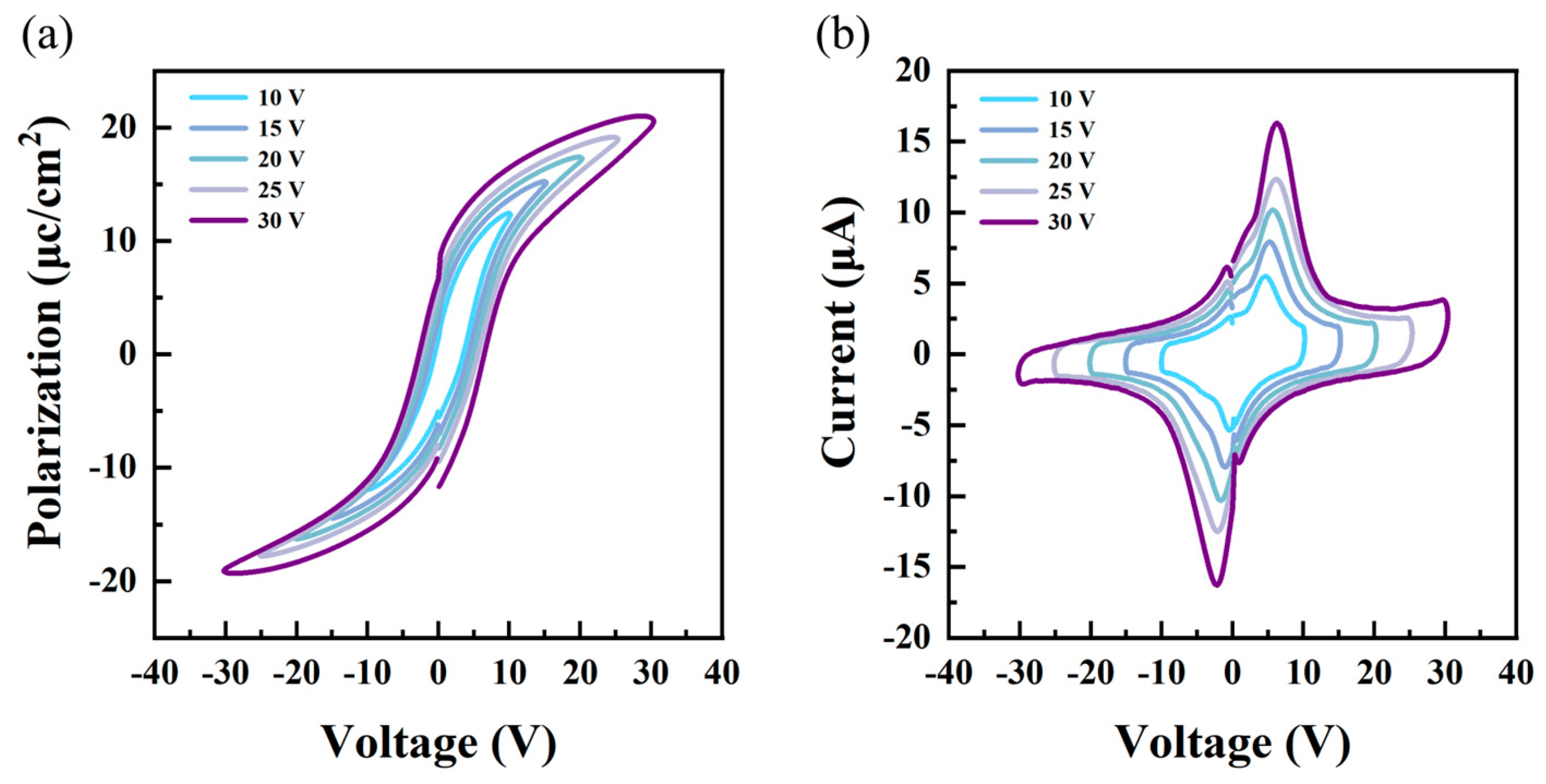
3.3. Study on Electrical Properties
4. Discussion
5. Conclusions
Supplementary Materials
Author Contributions
Funding
Data Availability Statement
Conflicts of Interest
References
- Ielmini, D.; Wong, H.S.P. In-memory computing with resistive switching devices. Nat. Electron. 2018, 1, 333–343. [Google Scholar] [CrossRef]
- Zidan, M.A.; Strachan, J.P.; Lu, W.D. The future of electronics based on memristive systems. Nat. Electron. 2018, 1, 22–29. [Google Scholar] [CrossRef]
- Neisser, M. International roadmap for devices and systems lithography roadmap. J. Micro/Nanopattern. Mater. Metrol. 2021, 20, 044601. [Google Scholar] [CrossRef]
- Jiang, J.; Chai, X.; Wang, C.; Jiang, A. High temperature ferroelectric domain wall memory. J. Alloys Compd. 2021, 856, 158155. [Google Scholar] [CrossRef]
- Choi, H.-Y.; Jeon, J.D.; Kim, S.E.; Jang, S.Y.; Sung, J.Y.; Lee, S.W. Strained BaTiO3 thin films via in-situ crystallization using atomic layer deposition on SrTiO3 substrate. Mater. Sci. Semicond. Process. 2023, 160, 107442. [Google Scholar] [CrossRef]
- Olgun, A.; Bostanci, F.N.; Francisco de Oliveira Junior, G.; Tugrul, Y.C.; Bera, R.; Yaglikci, A.G.; Hassan, H.; Ergin, O.; Mutlu, O. Sectored DRAM: A Practical Energy-Efficient and High-Performance Fine-Grained DRAM Architecture. ACM Trans. Archit. Code Optim. 2024, 21, 1–29. [Google Scholar] [CrossRef]
- Cao, Y.; Liu, Y.; Yang, Y.; Li, Q.; Zhang, T.; Ji, L.; Zhu, H.; Chen, L.; Sun, Q.; Zhang, D.W. Structural Engineering of H0.5Z0.5O2-Based Ferroelectric Tunneling Junction for Fast-Speed and Low-Power Artificial Synapses. Adv. Electron. Mater. 2023, 9, 2201247. [Google Scholar] [CrossRef]
- Wang, W.; Takai, K.; Eshita, T.; Nakabayashi, M.; Nakamura, K.; Oikawa, M.; Sato, N.; Suezawa, K.; Okita, Y.; Ozawa, S.; et al. Development of a High-Endurance Ferroelectric Capacitor for FeRAM in Automotive and Industrial Applications. IEEE Trans. Electron Devices 2025, 72, 629–634. [Google Scholar] [CrossRef]
- Kim, M.-K.; Kim, I.-J.; Lee, J.-S. Defect Engineering of Hafnia-Based Ferroelectric Materials for High-Endurance Memory Applications. ACS Omega 2023, 8, 18180–18185. [Google Scholar] [CrossRef]
- Bez, R.; Pirovano, A. Non-volatile memory technologies: Emerging concepts and new materials. Mater. Sci. Semicond. Process. 2004, 7, 349–355. [Google Scholar] [CrossRef]
- Li, Y.; Yang, Y.; Zhao, H.; Duan, H.; Yang, C.; Min, T.; Li, T. Nonvolatile Memory Device Based on the Ferroelectric Metal/Ferroelectric Semiconductor Junction. Nano Lett. 2025, 25, 1680–1688. [Google Scholar] [CrossRef] [PubMed]
- Jung, S.; Park, J.; Kim, J.; Song, W.; Jo, J.; Park, H.; Kong, M.; Kang, S.; Sheeraz, M.; Kim, I.W.; et al. Self-selective ferroelectric memory realized with semimetalic graphene channel. NPJ 2D Mater. Appl. 2021, 5, 90. [Google Scholar] [CrossRef]
- Li, C.; Huang, L.; Li, T.; Lü, W.; Qiu, X.; Huang, Z.; Liu, Z.; Zeng, S.; Guo, R.; Zhao, Y.; et al. Ultrathin BaTiO3-Based Ferroelectric Tunnel Junctions through Interface Engineering. Nano Lett. 2015, 15, 2568–2573. [Google Scholar] [CrossRef]
- Mikolajick, T.; Schroeder, U.; Slesazeck, S. The Past, the Present, and the Future of Ferroelectric Memories. IEEE Trans. Electron Devices 2020, 67, 1434–1443. [Google Scholar] [CrossRef]
- Ali, Z. FeRAM: A Paradigm of Advanced Data Storage Technology. Int. J. Res. Appl. Sci. Eng. Technol. 2023, 11, 1684–1691. [Google Scholar] [CrossRef]
- Chen, Y.; Wang, S.; Liu, F.; Wu, B.; Deng, Y.; Tao, R.; Wu, Y.; Gao, D. The working principle, structural design and material development of ferroelectric field-effect transistors and random-access memories. J. Alloys Compd. 2025, 1010, 178077. [Google Scholar] [CrossRef]
- Fu, D.; He, F.; Tian, H.; Li, J.; Zhang, J.; Kang, Z.; Wu, Y.; Wang, X. Ni-modified BaTiO3 film prepared by sol-gel with high energy storage performance. Ceram. Int. 2024, 50, 52004–52010. [Google Scholar] [CrossRef]
- Wang, W.; Fan, T.; Hu, S.; Zhang, J.; Zou, X.; Yang, Y.; Dou, Z.; Zhou, L.; Hu, J.; Wang, J.; et al. Defect Control of Donor Doping on Dielectric Ceramics to Improve the Colossal Permittivity and Temperature Stability. Coatings 2024, 14, 1024. [Google Scholar] [CrossRef]
- Chu, J.P.; Mahalingam, T.; Liu, C.F.; Wang, S.F. Preparation and characterization of Mn-doped BaTiO3 thin films by magnetron sputtering. J. Mater. Sci. 2006, 42, 346–351. [Google Scholar] [CrossRef]
- Kushwaha, A.K.; Khadka, R.; Keblinski, P. Surface-Induced effects in ferroelectric BaTiO3 thin films. Surf. Interfaces 2025, 56, 105589. [Google Scholar] [CrossRef]
- Takashima, H.; Katsumata, T.; Takebayashi, Y.; Ono, T.; Sue, K. Preparation of freestanding BaTiO3 nanocrystalline films and investigation of the effect of sintering on their dielectric properties. Ceram. Int. 2024, 50, 53753–53760. [Google Scholar] [CrossRef]
- Hao, Y.-J.; Gao, X.-Q.; Tang, Y.-C.; Xie, L.-T.; Xu, H.-Y.; Zhou, X.-X.; Hu, J.-H.; Liu, H.; Li, H.-Z.; Zhang, B.-P. Enhanced strain of BiFeO3-BaTiO3 relaxor ferroelectrics ceramics: Domain structure evolution induced by electric-fields and temperature. Rare Met. 2025, 44, 1–11. [Google Scholar] [CrossRef]
- Komatsu, K.; Suzuki, I.; Aoki, T.; Hamasaki, Y.; Yasui, S.; Itoh, M.; Taniyama, T. In-plane ferroelectricity and enhanced Curie temperature in perovskite BaTiO3 epitaxial thin films. Appl. Phys. Lett. 2020, 117, 072902. [Google Scholar] [CrossRef]
- Ogugua, S.N.; Ntwaeaborwa, O.M.; Swart, H.C. Latest Development on Pulsed Laser Deposited Thin Films for Advanced Luminescence Applications. Coatings 2020, 10, 1078. [Google Scholar] [CrossRef]
- Instan, A.A.; Pavunny, S.P.; Bhattarai, M.K.; Katiyar, R.S. Ultrahigh capacitive energy storage in highly oriented Ba(ZrxTi1 − x)O3 thin films prepared by pulsed laser deposition. Appl. Phys. Lett. 2017, 111, 142903. [Google Scholar] [CrossRef]
- Beklešovas, B.; Stankus, V.; Iljinas, A.; Balčiūnaitė, U. Enhancement of Ferroelectric Properties of Ni-Substituted Pb2Fe2O5 Thin Films Synthesized by Reactive Magnetron Sputtering Deposition. Coatings 2025, 15, 143. [Google Scholar] [CrossRef]
- Walke, A.M.; Popovici, M.I.; Sharifi, S.H.; Demir, E.C.; Puliyalil, H.; Bizindavyi, J.; Yasin, F.; Clima, S.; Fantini, A.; Belmonte, A.; et al. La Doped HZO-Based 3D-Trench Metal-Ferroelectric-Metal Capacitors With High-Endurance (>1012) for FeRAM Applications. IEEE Electron Device Lett. 2024, 45, 578–581. [Google Scholar] [CrossRef]
- Yaacoub, E.; Filali, F.; Abu-Dayya, A. QoE Enhancement of SVC Video Streaming Over Vehicular Networks Using Cooperative LTE/802.11p Communications. IEEE J. Sel. Top. Signal Process. 2015, 9, 37–49. [Google Scholar] [CrossRef]
- Ramdasi, O.A.; Kadhane, P.S.; Jadhav, T.K.; Dhotre, A.V.; Kolekar, Y.D.; Kambale, R.C. Improved Tc and ferroelectric fatigue characteristics of BaTiO3-rich (1 − x) BaTiO3 − (x) Bi0.5K0.5TiO3 lead-free electroceramics. J. Mater. Sci. Mater. Electron. 2024, 35, 1101. [Google Scholar] [CrossRef]
- Yang, Y.; Yuan, G.; Yan, Z.; Wang, Y.; Lu, X.; Liu, J.-M. Flexible, Semitransparent, and Inorganic Resistive Memory based on BaTi0.95Co0.05O3 Film. Adv. Mater. 2017, 29, 1700425. [Google Scholar] [CrossRef]
- Liu, X.; Wei, C.; Sun, T.; Zhang, F.; Li, H.; Liu, L.; Peng, Y.; Li, H.; Hong, M. A BaTiO3 − based flexible ferroelectric capacitor for non-volatile memories. J. Mater. 2025, 11, 100870. [Google Scholar] [CrossRef]
- Sun, H.; Luo, Z.; Zhao, L.; Liu, C.; Ma, C.; Lin, Y.; Gao, G.; Chen, Z.; Bao, Z.; Jin, X.; et al. BiFeO3-Based Flexible Ferroelectric Memristors for Neuromorphic Pattern Recognition. ACS Appl. Electron. Mater. 2020, 2, 1081–1089. [Google Scholar] [CrossRef]
- Lin, J.L.; He, R.; Lu, Z.; Lu, Y.; Wang, Z.; Zhong, Z.; Zhao, X.; Li, R.-W.; Zhang, Z.D.; Wang, Z.J. Oxygen vacancy enhanced ferroelectricity in BTO: SRO nanocomposite films. Acta Mater. 2020, 199, 9–18. [Google Scholar] [CrossRef]
- Hsu, M.-H.M.; Van Thourhout, D.; Pantouvaki, M.; Meersschaut, J.; Conard, T.; Richard, O.; Bender, H.; Favia, P.; Vila, M.; Cid, R.; et al. Controlled orientation of molecular-beam-epitaxial BaTiO3 on Si (001) using thickness engineering of BaTiO3 and SrTiO3 buffer layers. Appl. Phys. Express 2017, 10, 065501. [Google Scholar] [CrossRef]
- Ma, Q.; Kato, K. Anisotropy in morphology and crystal structure of BaTiO3 nanoblocks. Mater. Des. 2016, 107, 378–385. [Google Scholar] [CrossRef]
- Donohue, J.; Miller, S.J.; Cline, R.F. The effect of various substituents on the lattice constants of tetragonal titanate. Acta Crystallogr. 1958, 11, 693–695. [Google Scholar] [CrossRef]
- Kim, Y.S.; Kim, D.H.; Kim, J.D.; Chang, Y.J.; Noh, T.W.; Kong, J.H.; Char, K.; Park, Y.D.; Bu, S.D.; Yoon, J.G.; et al. Critical thickness of ultrathin ferroelectric BaTiO3 films. Appl. Phys. Lett. 2005, 86, 102907. [Google Scholar] [CrossRef]
- Michel, V.F.; Esswein, T.; Spaldin, N.A. Interplay between ferroelectricity and metallicity in BaTiO3. J. Mater. Chem. C Mater. 2021, 9, 8640–8649. [Google Scholar] [CrossRef]
- Zheng, H.; Wang, J.; Lofland, S.E.; Ma, Z.; Mohaddes-Ardabili, L.; Zhao, T.; Salamanca-Riba, L.; Shinde, S.R.; Ogale, S.B.; Bai, F.; et al. Multiferroic BaTiO3-CoFe2O4 Nanostructures. Science 2004, 303, 661. [Google Scholar] [CrossRef]
- Yang, Y.; Wu, M.; Li, X.; Hu, H.; Jiang, Z.; Li, Z.; Hao, X.; Zheng, C.; Lou, X.; Pennycook, S.J.; et al. The Role of Ferroelectric Polarization in Resistive Memory Properties of Metal/Insulator/Semiconductor Tunnel Junctions: A Comparative Study. ACS Appl. Mater. Interfaces 2020, 12, 32935–32942. [Google Scholar] [CrossRef]
- Botea, M.; Chirila, C.; Boni, G.A.; Pasuk, I.; Trupina, L.; Pintilie, I.; Hrib, L.M.; Nicu, B.; Pintilie, L. Lead-Free BiFeO3 Thin Film: Ferroelectric and Pyroelectric Properties. Electron. Mater. 2022, 3, 173–184. [Google Scholar] [CrossRef]
- Yi, X.; Duan, M.; Li, A.; Yang, G.; Zhang, W.; Jia, C. Synapse with Diverse Plasticity in Ferroelectric BaTiO3 Thin Films for Neuromorphic Computing. J. Phys. Chem. C 2024, 128, 2231–2239. [Google Scholar] [CrossRef]
- Kacem, H.; Sassi, Z.; Essid, M.; Dhahri, J.; Al-Harbi, N.; Alotaibi, B.M.; Alyousef, H.A. Energy storage performance and electrocaloric effect of Zr doped BaTiO3-based lead-free ferroelectric ceramics. Appl. Phys. A 2024, 130, 822. [Google Scholar] [CrossRef]


| Model | Stiffness * | Tip Radius | Manufacturer | Country of Origin |
|---|---|---|---|---|
| Multi75Al-G | 3 N/m | <10 nm | Budget Sensors | Bulgaria |
Disclaimer/Publisher’s Note: The statements, opinions and data contained in all publications are solely those of the individual author(s) and contributor(s) and not of MDPI and/or the editor(s). MDPI and/or the editor(s) disclaim responsibility for any injury to people or property resulting from any ideas, methods, instructions or products referred to in the content. |
© 2025 by the authors. Licensee MDPI, Basel, Switzerland. This article is an open access article distributed under the terms and conditions of the Creative Commons Attribution (CC BY) license (https://creativecommons.org/licenses/by/4.0/).
Share and Cite
Fang, Z.; Peng, Y.; Li, H.; Liu, X.; Zhai, J. High-Performance Ferroelectric Capacitors Based on Pt/BaTiO3/SrRuO3/SrTiO3 Heterostructures for Nonvolatile Memory Applications. Crystals 2025, 15, 337. https://doi.org/10.3390/cryst15040337
Fang Z, Peng Y, Li H, Liu X, Zhai J. High-Performance Ferroelectric Capacitors Based on Pt/BaTiO3/SrRuO3/SrTiO3 Heterostructures for Nonvolatile Memory Applications. Crystals. 2025; 15(4):337. https://doi.org/10.3390/cryst15040337
Chicago/Turabian StyleFang, Zengyuan, Yiming Peng, Haiou Li, Xingpeng Liu, and Jianghui Zhai. 2025. "High-Performance Ferroelectric Capacitors Based on Pt/BaTiO3/SrRuO3/SrTiO3 Heterostructures for Nonvolatile Memory Applications" Crystals 15, no. 4: 337. https://doi.org/10.3390/cryst15040337
APA StyleFang, Z., Peng, Y., Li, H., Liu, X., & Zhai, J. (2025). High-Performance Ferroelectric Capacitors Based on Pt/BaTiO3/SrRuO3/SrTiO3 Heterostructures for Nonvolatile Memory Applications. Crystals, 15(4), 337. https://doi.org/10.3390/cryst15040337