Article

Temperature-Dependent Spectroscopic Ellipsometry and Modeling of the Optical Properties of Vanadium Dioxide Thin Films

1
Department of Optical Science and Engineering, School of Information Science and Technology, State Key Laboratory of Photovoltaic Science and Technology, Fudan University, Shanghai 200433, China
2
Shanghai Key Laboratory of Optical Coatings and Spectral Modulation, Shanghai Institute of Technical Physics, Chinese Academy of Sciences, Shanghai 200083, China
3
High Tech Center for New Materials, Novel Devices and Cutting-Edge Manufacturing, Yiwu Research Institute, Fudan University, Yiwu 322000, China
4
Department of Physics, Quantum Photonic Science Research Center and RINS, Hanyang University, Seoul 04763, Republic of Korea
*
Authors to whom correspondence should be addressed.
Crystals 2025, 15(4), 325; https://doi.org/10.3390/cryst15040325
Submission received: 15 February 2025 / Revised: 19 March 2025 / Accepted: 25 March 2025 / Published: 28 March 2025
(This article belongs to the Section Inorganic Crystalline Materials)

Abstract

:
The metal–insulator transition of vanadium dioxide (VO2), a phase change material, has been utilized for various applications. The characterization of the VO2 thin film structure, in both its optical properties and thickness, remains a critical problem. In this paper, VO2 thin films were fabricated on silicon substrates by magnetron sputtering. By using temperature-varying spectroscopic ellipsometry, VO2 thin films of different thicknesses were characterized in an energy range of 0.5–3.0 eV, and the phase change temperature was determined using ellipsometry data. The optical properties of these samples were determined from temperature-dependent ellipsometry measurements by using the Drude and multiple Tauc–Lorentz model. Broadband temperature-dependent reflectivity spectra were obtained. An analysis of the samples revealed that their bandgaps, plasma frequencies, and other modeling parameters demonstrated a pattern of change with increasing temperature, which could be explained by the underlying physics. This study will help with the design of VO2-based structures for a broad range of applications.

1. Introduction

Vanadium dioxide (VO2), since being discovered in 1959 [1], has been one of the most favored phase change materials (PCMs) in the research community. As a PCM, VO2 exhibits a well-known metal–insulator transition (MIT), as well as a structural phase transition (SPT), which can be triggered by heating or cooling, as well as other stimuli such as strain, pressure, chemical doping and intense optical or electrostatic fields [2,3,4,5]. The MIT of VO2 occurs around a phase change temperature (PCT) of 68   ° C , which is easily accessible compared to many other PCMs. Furthermore, compared to PCMs which exhibit either MIT or SPT, vanadium dioxide can demonstrate these two mechanisms together. As such, researchers have been debating for a long time over the physical origin of this co-occurrence [6]. Despite the intrinsic physics, the separate properties of MIT and SPT have been well investigated [7,8,9,10,11,12,13]. To be more specific, below PCT and without strain, VO2 adopts a monoclinic structure, which can be denoted as the M1 phase (space group P21/c). While above 68   ° C , however, it exhibits a tetragonal rutile structure (R phase) with a different space group (P42/mnm). At the M1 phase, VO2 behaves like a typical semiconductor with relatively low reflection and absorption. When heated to the R phase, both reflection and absorption will increase, and it behaves like a typical metal. This drastic contrast of reflection and absorption is due to the changed electron behaviors at MIT and SPT, which also produce different physical properties at different phases, for example, electrical conductivity and optical constants.
These phase change properties of VO2 have attracted wide interest from researchers. Owing to its capability of exhibiting multi-stimuli responses and relatively low PCT, VO2 has found itself useful in many applications [14]. For example, VO2 demonstrates a good tradeoff between a high temperature coefficient of resistance (TCR) and a low resistivity, which correspond to high sensitivity and low thermal noise, respectively, and thus can be utilized as a detecting material in a bolometer [15]. It can also be useful as an optical switch [16,17], owing to its “quasi-instantaneous” response to optical pulses, which is promising in the application of high-power laser protection. Because of its Mott transition, stimulated by electrical pulses, VO2 can be used to construct memory devices [18,19], transistors [20] and memristors [21], as an essential material in next-generation neuromorphic nanoelectronics [22,23,24]. Last, but not least, VO2 has been identified as a thermochromic material for its temperature-varying response [25,26,27]. With an appropriate doping of high-valence metal ions (W6+, Mo6+ and Nb5+) to lower its PCT to near ambient temperature, VO2-based smart windows can self-modulate both solar heating and near-infrared radiation, and create a comfortable environment for human beings. As a thermochromic material, VO2 has also been intensively studied for smart radiative cooling recently [28]. By incorporating it into various structures, smart radiative coolers can turn their cooling capability on and off in response to surrounding environments. These applications show that VO2 possesses enormous potential as an intelligent matter and a high value in both research communities and industries.
Both complicated properties and broad applications call for precise and efficient characterization techniques for vanadium dioxide. Ellipsometry had its roots in the late 1800s, when Drude used the phase shift induced between mutually perpendicular components of polarized light to measure film thicknesses down to a few tens and ones of angstroms [29]. Thanks to the rise of integrated circuits and digital computers, various ellipsometer instruments have been designed and commercialized since the mid-1900s. Spectroscopic ellipsometry (SE) has become a well-recognized characterization technique, especially in the semiconductor manufacturing industry [30,31]. Ellipsometric investigations of VO2 can be dated back to 1985 [32]. However, owing to the famous “sample effects”, as denoted by Aspnes [33], optical constants obtained from ellipsometry measurements have varied from study to study. This is especially true for vanadium dioxide [34,35,36,37,38]. Many factors may lead to this variation, such as different substrates, synthesis methods, and fabrication constraints. Here, we prepared, by magnetron sputtering, three samples of VO2 thin films with different thicknesses, and performed temperature-dependent spectroscopic ellipsometry characterizations to determine their optical and surface properties. Temperature-dependent ellipsometry was also used as a novel method to determine the PCT of VO2, which is more reliable than resistivity measurements owing to its high accuracy and repeatability. Ultrabroadband temperature-dependent reflectivity characterizations at UV-vis-IR wavelengths were also conducted. We used auxiliary characterization techniques to verify the ellipsometric results, and further interpretation on the obtained optical constants was carried out to reveal the underlying physics.

2. Materials and Methods

Vanadium dioxide thin films of different thicknesses and crystallite sizes were prepared by magnetron sputtering. A high-purity (99.9%) vanadium target was purchased from ZhongNuo Advanced Material. Silicon wafer (crystal orientation 100, n-type) was used as the substrate. A gas mixture of argon (Ar) and O2 at a ratio of 50:1 was used. The sputtering pressure was maintained at 0.5   P a , and the substrate temperature was kept at 475   ° C . After the sputtering deposition, annealing was conducted in a vacuum furnace at 525   ° C to crystallize the film. Three different samples were made, with thicknesses of approximately 30, 50, and 80 nm (denoted as S1, S2, and S3, respectively). Accurate measurement of the thickness was made by ellipsometry and cross-sectional scanning electron microscopy (SEM).
Temperature-dependent spectroscopic ellipsometry was conducted on a V-VASE instrument (J. A. Woollam Co., Lincoln, NE, USA). All three samples were measured in the temperature range of 20 ~ 100   ° C . The photon energy range was 0.5–3.0 eV, with a step of 0.05   e V . To obtain more information from the measurements, we chose three incident angles ( 65 ° ,   70 ° ,   75 ° ). The redundancy of data may help with future fitting for the thickness and optical properties [29]. Temperature-dependent reflectivity spectra were measured with two sets of instruments, as follows: the shorter wavelengths (0.5–3.0 eV, corresponding to 400–2500 nm) on the ellipsometer itself, and the longer wavelengths (2.5–25 μm) on an FT-IR spectrometer (Vertex 70, Bruker, San Jose, CA, USA). A self-built thermal heating system was connected to the ellipsometer sample stage for temperature control. The crystalline phases of VO2 were determined by X-ray diffraction (XRD) (Ultima IV, Rigaku, Tokyo, Japan). We also performed auxiliary characterizations by SEM (Mira, Tescan, Brno, Czech Republic) and atomic force microscopy (AFM) (MultiMode 8, Bruker, USA) for straightforward inspection and surface mapping of the samples.

3. Results and Discussion

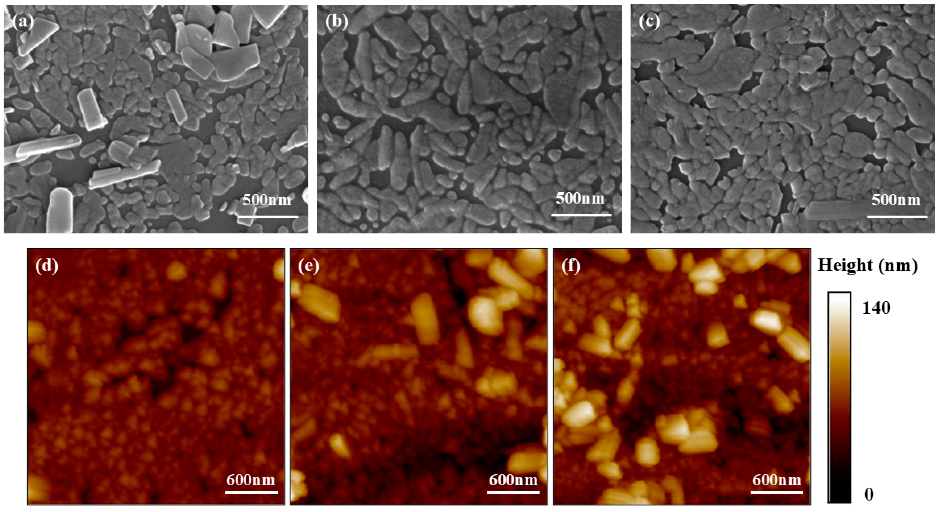
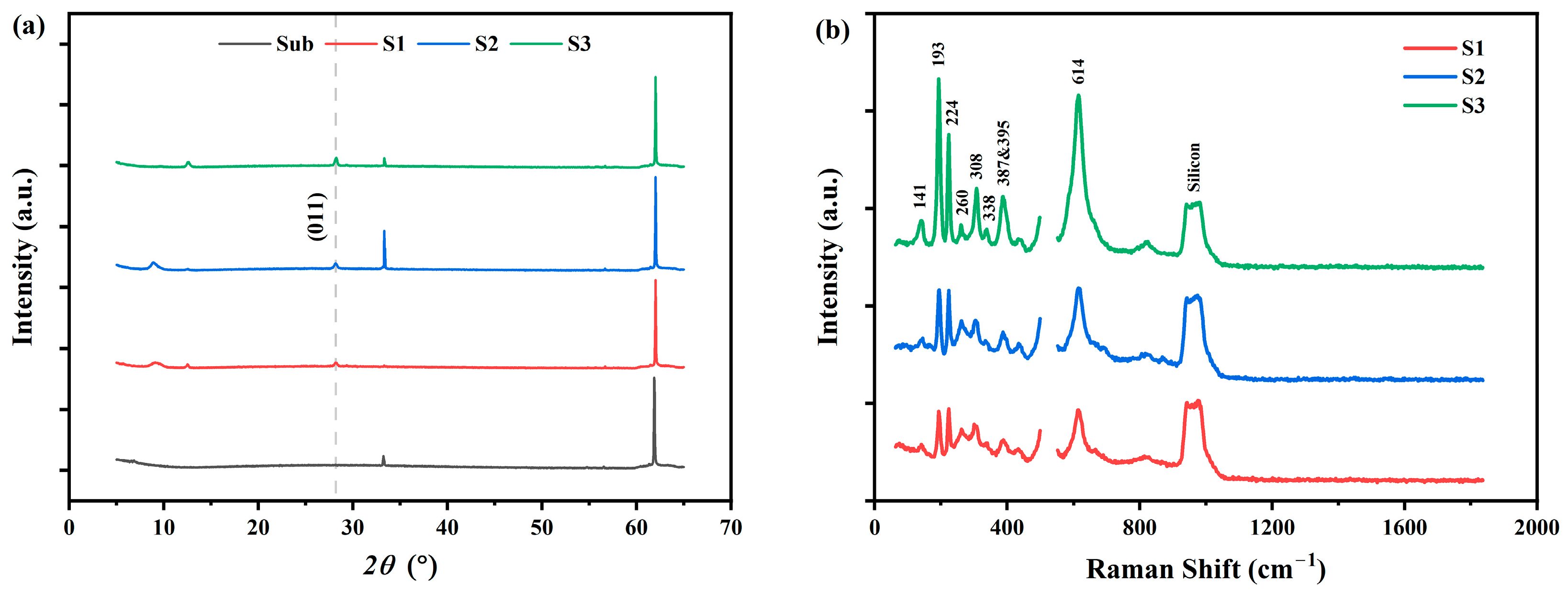
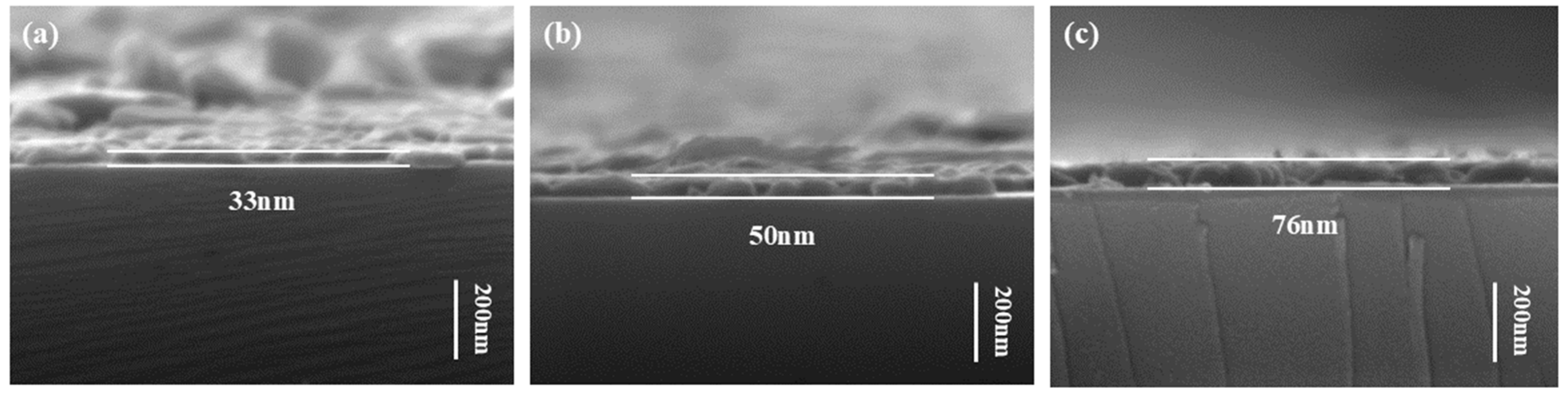
3.1. Surface Morphology

The surface SEM and AFM images of S1–S3 are shown in Figure 1. We can notice, from the SEM images, that the growth of VO2 film follows the Volmer–Weber mode [39]. Because of the film-substrate lattice mismatch, discrete islands form and grow until they impinge and coalesce with each other. According to the AFM images, the surface roughness increases with increasing thickness. Detailed mean surface roughness data of S1–S3 are listed in Table 1. XRD results of the silicon substrate (denoted as “Sub”) and samples S1–S3 are shown in Figure 2a. The diffraction peak at 27.8° was determined to be the (0, 1, 1) orientation of monoclinic VO2 with reference to PDF no. 44-0252. According to the Scherrer equation [40], the crystallite size D can be estimated from the full width of half maxima (FWHM) of the diffraction peak. The calculated mean average grain sizes D of S1–S3 are shown in Table 1, too. We can notice an increase in D from S1 to S3, which indicates an increase in grain size. This is in accordance with the aforementioned SEM and AFM results. Figure 2b shows the Raman scattering spectra of the three samples. Typical Raman peaks of VO2 (M1) are all detected and annotated in the graph [41]. Notice that for the sake of clarity, the strong Raman scattering peak of Si at around 520   c m 1 [34] is excluded.

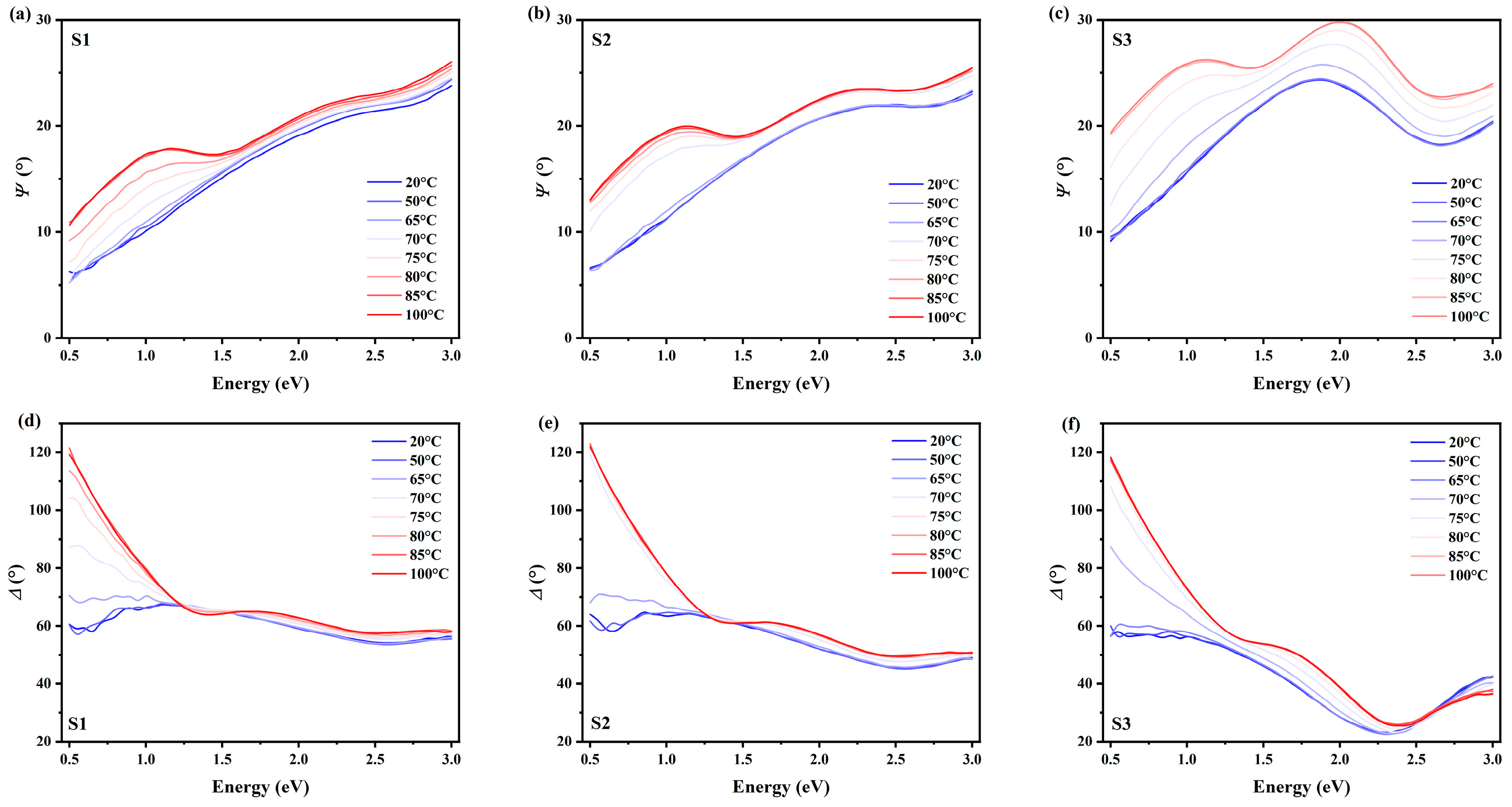
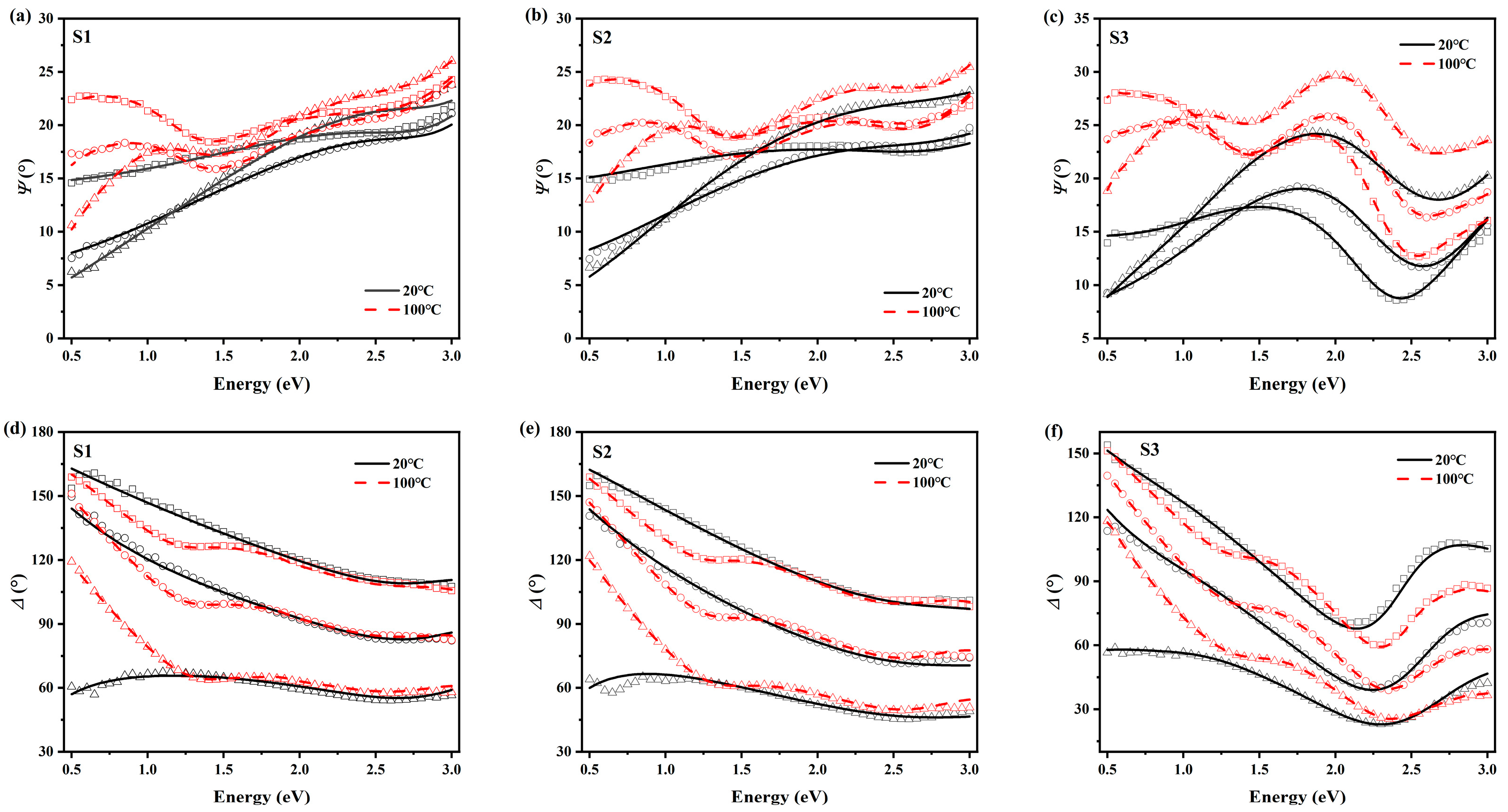
3.2. Temperature-Dependent Spectroscopic Ellipsometry

Spectroscopic ellipsometry is a characterization technique for determining the thickness and optical properties of thin films [29], and characterizing the critical dimensions (CD) of 3D microstructures [31,42]. The name “ellipsometry” comes from the fact that it utilizes elliptically polarized light as the detecting probe [43]. The change in polarization states during the reflection on the sample “reflects” sample properties. Two quantities are most frequently used in ellipsometry measurements: Ψ (psi) and Δ (delta). The tangent of Ψ is the ratio of the magnitudes of p-wave and s-wave reflection coefficients, and Δ is the phase shift induced by the reflection of the phase difference between the p-wave and s-wave:
tan Ψ = R p R s
Δ = δ 1 δ 2
where δ 1 and δ 2 are the phase difference before and after the reflection, respectively.
The temperature-varying ellipsometry results are depicted in Figure 3. For the sake of clarity, data of only one incident angle ( 75 ° ) is shown in the graph. The top and bottom panels show Ψ and Δ , respectively. From left to right, the three columns correspond to three samples, S1, S2, and S3. Colored lines in each graph indicate the continuous variations in the samples’ temperatures using the temperature-control system. We can notice that a similar trend of temperature-dependent phase change occurs for all three samples.
According to the temperature-dependent ellipsometric data, we can determine the phase transition temperature of VO2. Taking sample S2 as an example, the ellipsometric Ψ data at 1   e V is plotted against temperature, as shown in Figure 4a. As the temperature increases from 20 to 100   ° C , Ψ experiences an increase, and this change is the most abrupt around the phase transition temperature. Its first-order derivative is shown in Figure 4b, with a Gaussian fit (red line) for the center location at 68   ° C , which corresponds to the phase change temperature (PCT) of VO2 [7,34,44]. The determination of PCT using the temperature-dependent ellipsometry data is more reliable than the temperature-varying resistivity measurement, as ellipsometry is famous for its high accuracy and repeatability. Resistivity measurements, on the contrary, often suffer from irregular fluctuations and low generalizability [45,46]. As an auxiliary characterization, reflectivity spectra of vis-near-infrared (NIR) (400–2500 nm) and long-wave-infrared (LWIR) (2.5–25 μm) ranges are also measured, as plotted in Figure 4c,d. We can notice a strong temperature dependence across the infrared (IR) band (approximately 1–20 μm), which explains the wide application of VO2 at the infrared wavelengths. Here, the VO2 films were deposited on a silicon substrate, the bandgap of which is around 1.12   e V . The temperature-dependent reflection spectrum varies with the crystal phase of VO2. When VO2 is at the M1 phase, the film is almost transparent, leading to a low reflection. When it is heated and turns to the R phase, the reflection increases because of a drastic refractive index mismatch.
By combining Fresnel equations and Equations (1) and (2), we obtained thickness and optical property information of the sample from the ellipsometric data. Firstly, a model needs to be built for the unknown material layer (here, the VO2 layer), for both its dielectric constants and thickness. The average surface roughness layer is also considered with a thickness reference according to previous AFM measurements. The ellipsometric parameters ( Ψ and Δ ) can be calculated in a fully analytical way based on this model. Then, an optimization can be performed to reduce the root mean square error (RMSE) between the calculated and experimental Ψ and Δ . Here, the model we choose for the M1-phase VO2 (that is, below PCT) is the multiple Tauc–Lorentz oscillator model, as spikes occur occasionally in the dispersion curve of the imaginary part of the dielectric constants. Furthermore, compared to the classical Lorentz oscillator model, the Tauc–Lorentz model is capable of determining the bandgap of the material [47,48,49,50]. For the R-phase VO2 (above PCT), a Drude part is added to the multiple Tauc–Lorentz model to account for the free electron contribution after the MIT. Specifically, the Drude and multiple Tauc–Lorentz oscillator can be formulated as
ε ω = ε + ε D ω + k = 1 n ε T L , k ω
In Equation (3), the first term ε is a constant that denotes the contribution of the high-frequency electronic transition. ε D ω and ε T L , k ω refer to the Drude part and the k th Tauc–Lorentz oscillator, which can be further written as
ε D ω = ω p 2 ω 2 + i ω γ p
ε T L , k i m ω = 1 ω A k E 0 ,   k C k ω E g 2 ω 2 E 0 ,   k 2 2 + C k 2 ω 2 , E > E g 0 , E E g
ε T L , k r e ω = 2 π P E g ξ ε T L , k i m ξ ξ 2 ω 2 d ξ
In Equation (4), ω p = N e 2 / ε 0 m * 1 / 2 is the plasma frequency of R-phase VO2 ( N is the carrier density, and m * is the effective mass of electrons), and γ p is the broadening parameter which defines the scattering rate of free electrons. Equations (5) and (6) describe the imaginary and real part of the k th Tauc–Lorentz oscillator, where A k , E 0 ,   k , and C k are the amplitude, center energy, and broadening parameters, respectively, and E g is the bandgap energy. With ε T L , k i m ω , the real part ε T L , k r e ω can be calculated by the Kramers–Kronig integration, as detailed in Equation (6), where P is the representation of the Cauchy principal value integral.
The fitting results are shown in Figure 5. Only two temperatures are selectively shown (black solid lines for 20   ° C , and red dashed ones for 100   ° C ), and three lines in one set represent three incident angles. The experimental data and model fitting coincide well, except for some differences at the ends of the spectra, where the lack of redundant data affects the fitting accuracy. To testify the thickness accuracy, cross-sectional SEM is performed as an auxiliary characterization, as shown in Figure 6. We can notice that the actual thicknesses of the samples are in accordance with our expectations and fitting results.

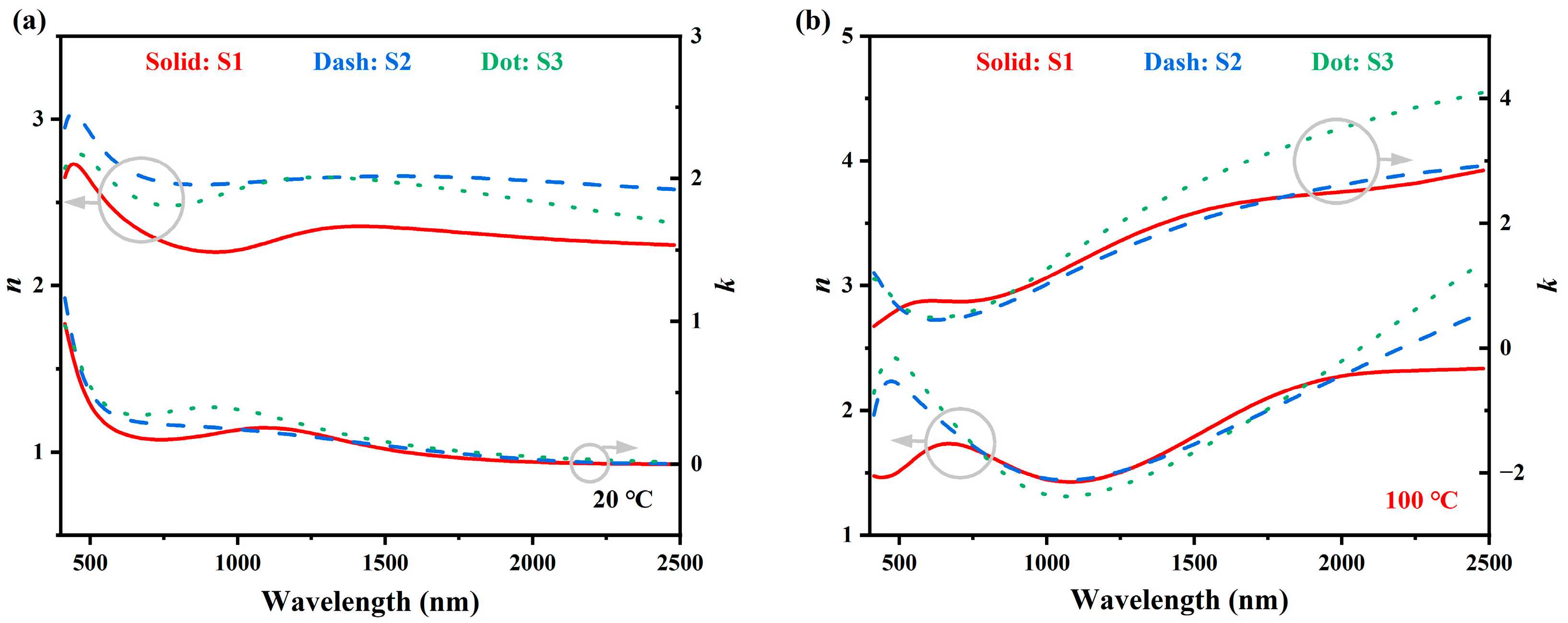
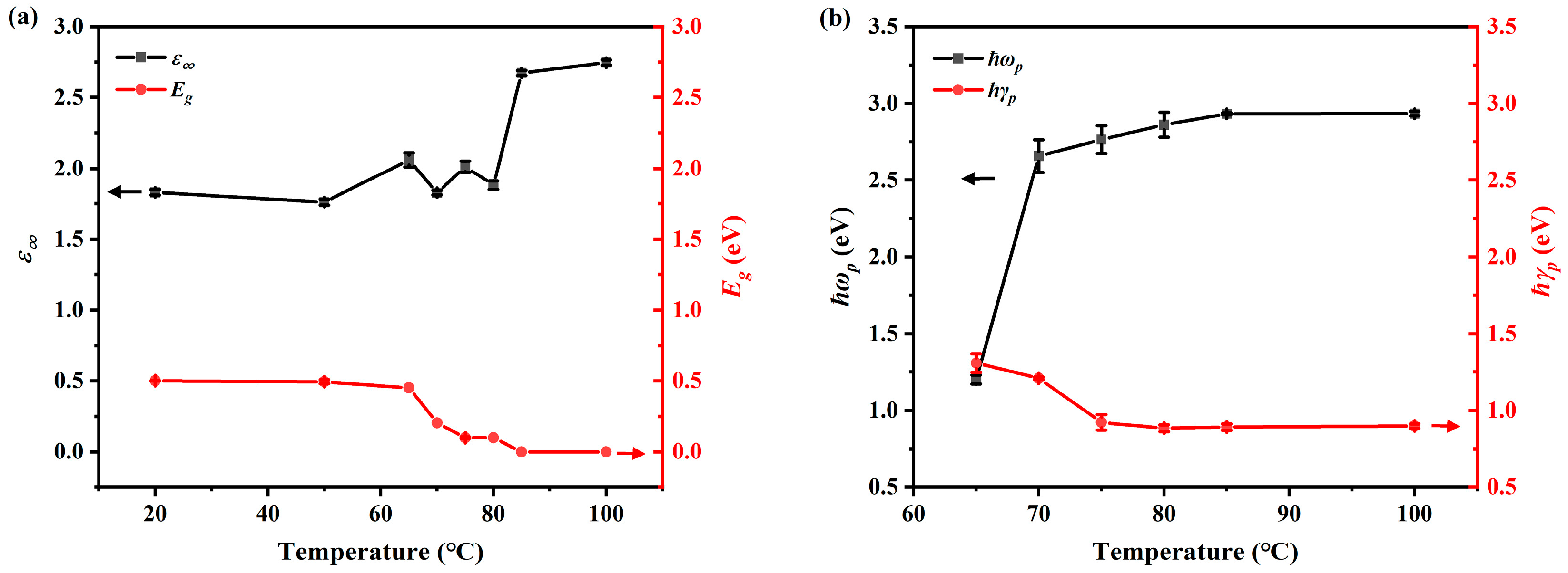
3.3. Optical Properties of Vanadium Dioxide

The optical properties of the M1 and R phase VO2 are extracted from the above-mentioned fitting models. Figure 7 shows the dielectric constants ( ε ) versus photon energy, and the left and right panels are the M1 phase ( 20   ° C ) and R phase ( 100   ° C ), respectively. In each graph, two sets of vertical axes are used to show the real part ( ε 1 ) and imaginary part ( ε 2 ), respectively. Solid red, dashed blue, and dotted green lines represent samples S1, S2, and S3, respectively. Similarly, in Figure 8, the optical constants ( n and k ) versus wavelengths are plotted. From these dispersion curves, some meaningful information can be extracted. Firstly, the bandgap E g , as determined by the Tauc–Lorentz model is approximately 0.5 eV, which is in accordance with previous publications [51]. When the temperature rises above 68   ° C , VO2 turns into R phase and responds like a semi-metal. The Drude part was used to describe this metal-like response.
The detailed fitting parameters of the Drude and Tauc–Lorentz model used for sample S2 are listed in Table 2. The RMSE of each optimization at different temperatures is also tabulated. Four model fitting parameters, the high-frequency term ε , the bandgap E g , the plasma frequency ω p , and the broadening parameter γ p , are plotted against temperature in Figure 9a,b. We can notice that ε and E g demonstrate a clear contrast before and after the phase transition. For the bandgap E g , the value of VO2 (M1) is around 0.5 eV, while for VO2 (R) it reduces to 0, which is in accordance with the phase change physics. In Figure 9b, plasma frequency ω p increases around the PCT, while the broadening parameter γ p decreases. This is because the free electron behaviors intensify with temperature increases and VO2 changes from M1 to R phase. However, a plateau begins to appear for both of them as the temperature reaches 85   ° C , indicating that the number of free electrons is beginning to saturate. This is because the phase transition is about to become complete at 85   ° C , which can also be noticed in direct experimental results, as is shown in Figure 3 and Figure 4c,d.

4. Conclusions

In this work, a series of vanadium dioxide (VO2) thin films were characterized by spectroscopic ellipsometry for a broad range of temperatures. The optical properties of M1 and R phase VO2 in a wavelength range from 0.5 to 3.0   e V and the film thicknesses were extracted through a multiple Tauc–Lorentz model and a Drude and multiple Tauc–Lorentz model, respectively. The phase change temperature was also obtained by calculating the first-order derivative of the ellipsometry data, which is a more reliable method owing to the high accuracy of the ellipsometry technic. Auxiliary measurements, such as XRD, Raman spectroscopy, SEM, AFM, and broadband temperature-dependent reflection spectroscopy, were carried out to ensure a self-consistent and comprehensive study. The bandgap of M1 phase VO2 was determined to be around 0.5 eV. We noticed an enhancement of free electron behavior with increasing temperature for R phase VO2, resulting in an increase in the plasma frequency and a decrease in the energy gap, which was explained by the underlying physics of the metal–insulator transition (MIT) of VO2. This study is promising for the potential application of VO2-based photonic and optoelectronic devices.

Supplementary Materials

The following supporting information can be downloaded at: https://www.mdpi.com/article/10.3390/cryst15040325/s1, Figure S1: Schematic of the temperature-dependent spectroscopic ellipsometry setup. Samples are mounted onto the ellipsometer stage with a hot plate, where the samples are heated by the inside copper heater, and the temperature is controlled by a thermocouple connected to the temperature monitor.; Figure S2: Surface and cross-sectional SEM images of samples S4 and S5, with a thickness of around 100 and 150 nm, respectively. Figure S3: Low and High temperature spectroscopic ellipsometry measured on S4 and S5. Figure S4: Optical properties of sample S4 and S5 extracted from the ellipsometric data. (a) and (b) show the real and imaginary part of the dielectric constant, (c) and (d) show the refractive index and extinction coefficient, respectively. Figure S5: The full Mueller matrix of sample S2. All off-diagonal entries are zero, which testify the isotropy of the samples.

Author Contributions

Conceptualization, X.S., Q.C. and Y.Z.; Data curation, X.S. and Q.C.; Formal analysis, X.S. and Y.Z.; Funding acquisition, Q.C., Y.Z., Y.L., J.L. and S.W.; Investigation, X.S., J.Q. and B.L.; Methodology, X.S., Q.C. and Y.Z.; Project administration, Q.C., R.Z., Y.Z., L.C., Y.L., J.L. and S.W.; Resources, Q.C., R.Z., Y.Z., L.C., Y.L., J.L. and S.W.; Software, X.S.; Supervision, Q.C., R.Z., Y.Z., L.C. and Y.L.; Validation, X.S.; Visualization, X.S.; Writing—original draft, X.S.; Writing—review and editing, Q.C., Y.Z. and Y.L. All authors have read and agreed to the published version of the manuscript.

Funding

This work was funded by the National Natural Science Foundation of China (62275053, 62275256, U2230108, 61427815, 11674062), the Eastern Talent Plan Youth Project 2022, the Open Fund of Shanghai Key Laboratory of Optical Coatings and Spectral Modulation and the Science and Technology Commission of Shanghai Municipality (STCSM-22142200200).

Data Availability Statement

Data are contained within the article or supplementary material.

Conflicts of Interest

The authors declare no conflicts of interest.

Abbreviations

The following abbreviations are used in this manuscript:
PCMPhase change material
MITMetal–insulator transition
PCTPhase change temperature
SEMScanning electron microscopy
AFMAtomic force microscopy
FWHMFull width of half maxima
RMSERoot mean square error

References

  1. Morin, F.J. Oxides Which Show a Metal-to-Insulator Transition at the Neel Temperature. Phys. Rev. Lett. 1959, 3, 34–36. [Google Scholar] [CrossRef]
  2. Gong, Z.; Yang, F.; Wang, L.; Chen, R.; Wu, J.; Grigoropoulos, C.P.; Yao, J. Phase change materials in photonic devices. J. Appl. Phys. 2021, 129, 030902. [Google Scholar] [CrossRef]
  3. Ke, Y.; Wang, S.; Liu, G.; Li, M.; White, T.J.; Long, Y. Vanadium Dioxide: The Multistimuli Responsive Material and Its Applications. Small 2018, 14, 1802025. [Google Scholar] [CrossRef]
  4. Liu, K.; Lee, S.; Yang, S.; Delaire, O.; Wu, J. Recent progresses on physics and applications of vanadium dioxide. Mater. Today 2018, 21, 875–896. [Google Scholar] [CrossRef]
  5. Bhupathi, S.; Wang, S.; Ke, Y.; Long, Y. Recent progress in vanadium dioxide: The multi-stimuli responsive material and its applications. Mater. Sci. Eng. R Rep. 2023, 155, 100747. [Google Scholar] [CrossRef]
  6. Weber, C.; O’Regan, D.D.; Hine, N.D.M.; Payne, M.C.; Kotliar, G.; Littlewood, P.B. Vanadium Dioxide: A Peierls-Mott Insulator Stable against Disorder. Phys. Rev. Lett. 2012, 108, 256402. [Google Scholar] [CrossRef] [PubMed]
  7. Barker, A.S.; Verleur, H.W.; Guggenheim, H.J. Infrared Optical Properties of Vanadium Dioxide Above and Below the Transition Temperature. Phys. Rev. Lett. 1966, 17, 1286–1289. [Google Scholar] [CrossRef]
  8. Whittaker, L.; Patridge, C.J.; Banerjee, S. Microscopic and Nanoscale Perspective of the Metal−Insulator Phase Transitions of VO2: Some New Twists to an Old Tale. J. Phys. Chem. Lett. 2011, 2, 745–758. [Google Scholar] [CrossRef]
  9. Kats, M.A.; Blanchard, R.; Zhang, S.; Genevet, P.; Ko, C.; Ramanathan, S.; Capasso, F. Vanadium Dioxide as a Natural Disordered Metamaterial: Perfect Thermal Emission and Large Broadband Negative Differential Thermal Emittance. Phys. Rev. X 2013, 3, 041004. [Google Scholar] [CrossRef]
  10. Kana Kana, J.B.; Vignaud, G.; Gibaud, A.; Maaza, M. Thermally driven sign switch of static dielectric constant of VO2 thin film. Opt. Mater. 2016, 54, 165–169. [Google Scholar] [CrossRef]
  11. Shao, Z.; Cao, X.; Luo, H.; Jin, P. Recent progress in the phase-transition mechanism and modulation of vanadium dioxide materials. NPG Asia Mater. 2018, 10, 581–605. [Google Scholar] [CrossRef]
  12. Wang, P.-F.; Hu, Q.; Zheng, T.; Liu, Y.; Xu, X.; Sun, J.-L. Optically Monitored Electric-Field-Induced Phase Transition in Vanadium Dioxide Crystal Film. Crystals 2020, 10, 764. [Google Scholar] [CrossRef]
  13. Polak, P.; Jamroz, J.; Pietrzak, T.K. Observation of Metal–Insulator Transition (MIT) in Vanadium Oxides V2O3 and VO2 in XRD, DSC and DC Experiments. Crystals 2023, 13, 1299. [Google Scholar] [CrossRef]
  14. Haddad, E.; Kruzelecky, R.V.; Murzionak, P.; Jamroz, W.; Tagziria, K.; Chaker, M.; Ledrogoff, B. Review of the VO2 smart material applications with emphasis on its use for spacecraft thermal control. Front. Mater. 2022, 9, 1013848. [Google Scholar] [CrossRef]
  15. Jiang, W.; Zheng, T.; Wu, B.; Jiao, H.; Wang, X.; Chen, Y.; Zhang, X.; Peng, M.; Wang, H.; Lin, T.; et al. A versatile photodetector assisted by photovoltaic and bolometric effects. Light Sci. Appl. 2020, 9, 160. [Google Scholar] [CrossRef]
  16. Zhou, Y.; Chen, X.; Ko, C.; Yang, Z.; Mouli, C.; Ramanathan, S. Voltage-Triggered Ultrafast Phase Transition in Vanadium Dioxide Switches. IEEE Electron Device Lett. 2013, 34, 220–222. [Google Scholar] [CrossRef]
  17. Wang, H.; Yi, X.; Li, Y. Fabrication of VO2 films with low transition temperature for optical switching applications. Opt. Commun. 2005, 256, 305–309. [Google Scholar] [CrossRef]
  18. Lee, M.-J.; Park, Y.; Suh, D.-S.; Lee, E.-H.; Seo, S.; Kim, D.-C.; Jung, R.; Kang, B.-S.; Ahn, S.-E.; Lee, C.B.; et al. Two Series Oxide Resistors Applicable to High Speed and High Density Nonvolatile Memory. Adv. Mater. 2007, 19, 3919–3923. [Google Scholar] [CrossRef]
  19. Pellegrino, L.; Manca, N.; Kanki, T.; Tanaka, H.; Biasotti, M.; Bellingeri, E.; Siri, A.S.; Marré, D. Multistate Memory Devices Based on Free-standing VO2/TiO2 Microstructures Driven by Joule Self-Heating. Adv. Mater. 2012, 24, 2929–2934. [Google Scholar] [CrossRef]
  20. Shukla, N.; Thathachary, A.V.; Agrawal, A.; Paik, H.; Aziz, A.; Schlom, D.G.; Gupta, S.K.; Engel-Herbert, R.; Datta, S. A steep-slope transistor based on abrupt electronic phase transition. Nat. Commun. 2015, 6, 7812. [Google Scholar] [CrossRef]
  21. Yi, W.; Tsang, K.K.; Lam, S.K.; Bai, X.; Crowell, J.A.; Flores, E.A. Biological plausibility and stochasticity in scalable VO2 active memristor neurons. Nat. Commun. 2018, 9, 4661. [Google Scholar] [CrossRef]
  22. Andrews, J.L.; Santos, D.A.; Meyyappan, M.; Williams, R.S.; Banerjee, S. Building Brain-Inspired Logic Circuits from Dynamically Switchable Transition-Metal Oxides. Trends Chem. 2019, 1, 711–726. [Google Scholar] [CrossRef]
  23. Sangwan, V.K.; Hersam, M.C. Neuromorphic nanoelectronic materials. Nat. Nanotechnol. 2020, 15, 517–528. [Google Scholar] [CrossRef]
  24. Kumar, S.; Wang, X.; Strachan, J.P.; Yang, Y.; Lu, W.D. Dynamical memristors for higher-complexity neuromorphic computing. Nat. Rev. Mater. 2022, 7, 575–591. [Google Scholar] [CrossRef]
  25. Cui, Y.; Ke, Y.; Liu, C.; Chen, Z.; Wang, N.; Zhang, L.; Zhou, Y.; Wang, S.; Gao, Y.; Long, Y. Thermochromic VO2 for Energy-Efficient Smart Windows. Joule 2018, 2, 1707–1746. [Google Scholar] [CrossRef]
  26. Xu, F.; Cao, X.; Luo, H.; Jin, P. Recent advances in VO2-based thermochromic composites for smart windows. J. Mater. Chem. C 2018, 6, 1903–1919. [Google Scholar] [CrossRef]
  27. Kamalisarvestani, M.; Saidur, R.; Mekhilef, S.; Javadi, F.S. Performance, materials and coating technologies of thermochromic thin films on smart windows. Renew. Sustain. Energy Rev. 2013, 26, 353–364. [Google Scholar] [CrossRef]
  28. An, Y.; Fu, Y.; Dai, J.-G.; Yin, X.; Lei, D. Switchable radiative cooling technologies for smart thermal management. Cell Rep. Phys. Sci. 2022, 3, 101098. [Google Scholar] [CrossRef]
  29. Hilfiker, J.; Tompkins, H. Spectroscopic Ellipsometry: Practical Application to Thin Film Characterization; Momentum Press: New York, NY, USA, 2016. [Google Scholar]
  30. Orji, N.G.; Badaroglu, M.; Barnes, B.M.; Beitia, C.; Bunday, B.D.; Celano, U.; Kline, R.J.; Neisser, M.; Obeng, Y.; Vladar, A.E. Metrology for the next generation of semiconductor devices. Nat. Electron. 2018, 1, 532–547. [Google Scholar] [CrossRef]
  31. Chen, X.; Liu, S. Optical Scatterometry for Nanostructure Metrology. In Metrology; Gao, W., Ed.; Springer: Singapore, 2019; pp. 1–37. [Google Scholar]
  32. Swann, J.T.; De Smet, D.J. Ellipsometric investigation of vanadium dioxide films. J. Appl. Phys. 1985, 58, 1335–1338. [Google Scholar] [CrossRef]
  33. Aspnes, D.E.; Kinsbron, E.; Bacon, D.D. Optical properties of Au: Sample effects. Phys. Rev. B 1980, 21, 3290–3299. [Google Scholar] [CrossRef]
  34. Wan, C.; Zhang, Z.; Woolf, D.; Hessel, C.M.; Rensberg, J.; Hensley, J.M.; Xiao, Y.; Shahsafi, A.; Salman, J.; Richter, S.; et al. On the Optical Properties of Thin-Film Vanadium Dioxide from the Visible to the Far Infrared. Ann. Der Phys. 2019, 531, 1900188. [Google Scholar] [CrossRef]
  35. Huang, Y.; Zhang, D.; Liu, Y.; Jin, J.; Yang, Y.; Chen, T.; Guan, H.; Fan, P.; Lv, W. Phase transition analysis of thermochromic VO2 thin films by temperature-dependent Raman scattering and ellipsometry. Appl. Surf. Sci. 2018, 456, 545–551. [Google Scholar] [CrossRef]
  36. Houska, J.; Kolenaty, D.; Rezek, J.; Vlcek, J. Characterization of thermochromic VO2 (prepared at 250 °C) in a wide temperature range by spectroscopic ellipsometry. Appl. Surf. Sci. 2017, 421, 529–534. [Google Scholar] [CrossRef]
  37. Kakiuchida, H.; Jin, P.; Nakao, S.; Tazawa, M. Optical Properties of Vanadium Dioxide Film during Semiconductive–Metallic Phase Transition. Jpn. J. Appl. Phys. 2007, 46, L113. [Google Scholar] [CrossRef]
  38. Petit, C.; Frigerio, J. Optical properties of VO2 thin films in their dielectric and metallic states. In Proceedings of the Optical Systems Design and Production, Berlin, Germany, 26–29 May 1999; Volume 3738. [Google Scholar]
  39. Floro, J.A.; Hearne, S.J.; Hunter, J.A.; Kotula, P.; Chason, E.; Seel, S.C.; Thompson, C.V. The dynamic competition between stress generation and relaxation mechanisms during coalescence of Volmer–Weber thin films. J. Appl. Phys. 2001, 89, 4886–4897. [Google Scholar] [CrossRef]
  40. Holzwarth, U.; Gibson, N. The Scherrer equation versus the ‘Debye-Scherrer equation’. Nat. Nanotechnol. 2011, 6, 534. [Google Scholar] [CrossRef]
  41. Schilbe, P. Raman scattering in VO2. Phys. B Condens. Matter 2002, 316–317, 600–602. [Google Scholar] [CrossRef]
  42. Huang, H.-T.; Kong, W.; Terry, F.L., Jr. Normal-incidence spectroscopic ellipsometry for critical dimension monitoring. Appl. Phys. Lett. 2001, 78, 3983–3985. [Google Scholar] [CrossRef]
  43. Vedam, K. Spectroscopic ellipsometry: A historical overview. Thin Solid Films 1998, 313–314, 1–9. [Google Scholar] [CrossRef]
  44. Nag, J.; Haglund, R.F. Synthesis of vanadium dioxide thin films and nanoparticles. J. Phys. Condens. Matter 2008, 20, 264016. [Google Scholar] [CrossRef]
  45. Valdes, L.B. Resistivity Measurements on Germanium for Transistors. Proc. IRE 1954, 42, 420–427. [Google Scholar] [CrossRef]
  46. Chelly, A.; Glass, S.; Belhassen, J.; Karsenty, A. Broad review of four-point probe correction factors: Enhanced analytical model using advanced numerical and experimental cross-examination. Results Phys. 2023, 48, 106445. [Google Scholar] [CrossRef]
  47. Tauc, J.; Grigorovici, R.; Vancu, A. Optical Properties and Electronic Structure of Amorphous Germanium. Phys. Status Solidi (B) 1966, 15, 627–637. [Google Scholar] [CrossRef]
  48. Likhachev, D.V.; Malkova, N.; Poslavsky, L. Modified Tauc–Lorentz dispersion model leading to a more accurate representation of absorption features below the bandgap. Thin Solid Films 2015, 589, 844–851. [Google Scholar] [CrossRef]
  49. Fujiwara, H. Appendix 2: Definitions of Optical Constants. In Spectroscopic Ellipsometry; John Wiley & Sons: Hoboken, NJ, USA, 2007; pp. 347–348. [Google Scholar]
  50. Collins, R.W.; Ferlauto, A.S. 2—Optical Physics of Materials. In Handbook of Ellipsometry; Tompkins, H.G., Irene, E.A., Eds.; William Andrew Publishing: Norwich, NY, USA, 2005; pp. 93–235. [Google Scholar]
  51. Abdelkadir, A.A.; Victor, J.-L.; Vignaud, G.; Marcel, C.; Sahal, M.; Maaza, M.; Chaker, M.; Gibaud, A. Analysis of the temperature dependent optical properties of V1−xWxO2 thin films. Thin Solid Films 2023, 772, 139805. [Google Scholar] [CrossRef]
Figure 1. (ac) Surface SEM and (df) AFM images of the three samples. (a,d) are for S1; (b,e) for S2; and (c,f) for S3. Color bar at the right of the AFM images shows the surface height.
Crystals 15 00325 g001
Figure 2. XRD and Raman spectroscopy results. (a) XRD of the silicon substrate (“Sub” in black line) and S1–S3 (red, blue, and green lines, respectively). The dashed line denotes the (0, 1, 1) plane of the M1 phase VO2 at 27.8°. (b) Raman spectra of the three samples (red, blue, and green lines for S1, S2, and S3, respectively). A strong peak of Si at 520   c m 1 was excluded for the sake of clarity. The characteristic Raman peaks of VO2 are annotated in the figure.
Crystals 15 00325 g002
Figure 3. Temperature-varying ellipsometry measurement results. The measurement was conducted at an incident angle of 75 ° . Top and bottom panels show Ψ and Δ , respectively. (a,d) are for sample S1; (b,e) for S2; and (c,f) for S3.
Crystals 15 00325 g003
Figure 4. Phase change temperature (PCT) and reflectivity spectra of sample S2. (a) shows the Ψ curve at 1 eV of S2 versus the temperature. (b) shows the first-order derivative of (a). The red line is the Gaussian fit curve, and the dashed line denotes the PCT at 68   ° C . (c,d) depict the reflectivity spectra in the vis-NIR and LWIR, respectively.
Crystals 15 00325 g004
Figure 5. Ellipsometric fitting results. (ac) are the ellipsometry angle Ψ of S1, S2, and S3, respectively. (df) are the ellipsometry angle Δ of S1, S2, and S3, respectively. Lines denote the fitting curves; symbols are for experimental data. The black solid and red dashed lines are for the temperatures of 20   ° C and 100   ° C , respectively. The square, circle, and triangle symbols represent incident angles of 65 ° ,   70 ° ,   a n d   75 ° respectively.
Crystals 15 00325 g005
Figure 6. Cross-sectional SEM images of the samples. (ac) represent S1, S2, and S3, respectively. The film thickness with respect to the scale bar is denoted in the image.
Crystals 15 00325 g006
Figure 7. Dielectric constants ( ε ) of the three samples. (a) M1-phase VO2 at 20   ° C ; (b) R-phase VO2 at 100   ° C . The left and right axes are for the real and imaginary part of ε , respectively. Solid red, dashed blue, and dotted green lines represent samples S1, S2, and S3, respectively.
Crystals 15 00325 g007
Figure 8. Optical constants ( n and k ) of the three samples. (a) M1-phase VO2 at 20   ° C . (b) R-phase VO2 at 100   ° C . The left and right axes are for the refractive index n and extinction coefficient k , respectively. Solid red, dash blue and dot green lines represent sample S1, S2 and S3, respectively.
Crystals 15 00325 g008
Figure 9. Evolution of the fitted model parameters of S2 VO2 with temperature. Error bars were calculated according to small variations in the surface roughness and layer thickness. (a) High-frequency term, ε , and the bandgap, E g , for sample S2 at different temperatures. (b) Plasma frequency, ω p , and broadening parameter, γ p , of sample S2 at different temperatures.
Crystals 15 00325 g009
Table 1. Parameters of the three samples. R a represents the average surface roughness measured by AFM. (h, k, l) is the preferred orientation of the sample. D is the crystallite size calculated by the Scherrer equation.
Sample R a (nm)(h, k, l)FWHM (°)D (nm)
S16.19(0, 1, 1)0.3821
S212.0(0, 1, 1)0.3622
S315.3(0, 1, 1)0.2927
Table 2. Detailed fitted model parameters of sample S2 at different temperatures. RMSE is the root mean square error during the fitting optimization procedure.
T (°C)20506570758085100
ε 1.831.762.061.832.011.882.672.75
ω p /eV//1.202.662.762.862.932.93
γ p /eV//1.311.210.920.880.890.90
E g /eV0.500.490.450.200.100.1000
RMSE0.6670.6690.7191.0721.2431.1051.0591.056
Disclaimer/Publisher’s Note: The statements, opinions and data contained in all publications are solely those of the individual author(s) and contributor(s) and not of MDPI and/or the editor(s). MDPI and/or the editor(s) disclaim responsibility for any injury to people or property resulting from any ideas, methods, instructions or products referred to in the content.

