Review

Electrically Active Defects in 3C, 4H, and 6H Silicon Carbide Polytypes: A Review

Ruđer Bošković Institute, Bijenička 54, 10 000 Zagreb, Croatia
Crystals 2025, 15(3), 255; https://doi.org/10.3390/cryst15030255
Submission received: 20 February 2025 / Revised: 6 March 2025 / Accepted: 8 March 2025 / Published: 10 March 2025

Abstract

:
This paper aims to critically review electrically active defects studied by junction spectroscopy techniques (deep-level transient spectroscopy and minority carrier transient spectroscopy) in the three most commonly used silicon carbide (SiC) polytypes: 3C-SiC, 4H-SiC, and 6H-SiC. Given the dominant role of SiC in power electronic devices, the focus is strictly on electrically active defects that influence material performance and device reliability. The most prevalent defects in each polytype and their effects on electrical properties will be examined. Additionally, recent advancements in defect characterization and defect engineering will be highlighted, emphasizing their impact on improving SiC-based device performance. The paper will also address the main challenges that continue to hinder the broader adoption of SiC, such as defect-related limitations in carrier lifetime and doping efficiency. Furthermore, beyond the well-established applications of SiC in power electronics and high-temperature environments, lesser-known niche applications will be explored, showcasing the material’s versatility in emerging fields.

1. Introduction

Semiconductors are the pillars of modern electronics, a driving force bringing innovations in different industries, from consumer electronics to renewable energy systems. As global demand for energy-efficient and high-performance devices continuously grows, traditional silicon-based devices face limitations in handling the increasingly stringent requirements of high-power, high-temperature, and high-frequency applications. These challenges have spurred widespread interest in alternative semiconductor materials, among which silicon carbide (SiC) has emerged as a game-changer. Silicon carbide is a wide bandgap semiconductor with unique material properties, such as a large critical electric field, high thermal conductivity, high electron saturation velocity, chemical inertness, and radiation hardness [1]. These properties make SiC-based devices far superior to their silicon counterparts for demanding applications. Furthermore, SiC has already established itself as a critical enabler of advancements in power electronics, where its capabilities have driven breakthroughs in efficiency and performance [2,3,4]. Recent progress in producing high-quality SiC wafers has opened the door to additional applications, including quantum technologies [5,6,7] and radiation detection [8,9,10,11,12,13], further solidifying SiC’s pivotal role in next-generation semiconductor technology.
The most commonly used SiC polytypes are 3C-, 4H-, and 6H-SiC. Accordingly, this literature review focuses on these three polytypes. Table 1 summarizes the fundamental material properties of 3C, 4H, and 6H-SiC [14,15].
The crystal structures for 3C-SiC (cubic), 6H-SiC (hexagonal), and 4H-SiC (hexagonal) with the associated staking sequences are shown in Figure 1. More details on SiC crystal structures can be found in Ref. [15] and the references therein.
Despite the abundance of original research papers and numerous SiC-related literature reviews, focused review articles that provide a comparative overview of the 3C, 4H-, and 6H-SiC polytypes remain surprisingly scarce. Among the limited number of such reviews, a few stand out and are highly recommended:
(i)
“Deep Defect Centers in Silicon Carbide Monitored with Deep Level Transient Spectroscopy“ by Dalibor et al. [17]. This comprehensive review examined electrical data obtained from DLTS investigations on deep defect centers in various SiC polytypes. The study provided a comparative analysis of deep-level defects across different SiC polytypes, aiding in the broader understanding of defect physics in SiC materials.
(ii)
“Comparative Study on Silicon Carbide (SiC) Polytypes in High Voltage Devices” by W. Taha [18]. This paper reviews the crystallography of major SiC polytypes and their electrical properties, presenting a material physical model and discussing their applications in high-voltage devices.
(iii)
“Electron Mobility in Bulk n-Doped SiC-Polytypes 3C-SiC, 4H-SiC, and 6H-SiC: A Comparison” by C.G. Rodriguez [19]. This study presents a comparative analysis of charge transport in bulk n-type doped SiC polytypes, focusing on electron drift velocity and mobility under varying electric field intensities and orientations.
(iv)
“A Comparative Study of Schottky Barrier Heights and Charge Transport in SiC Polytypes” by Mekaret et al. [20]. This paper presents a comparative analysis of Schottky diodes using three SiC polytypes (3C, 4H, and 6H), focusing on Schottky barrier heights and charge transport mechanisms.
(v)
”Comparison of 6H-SiC, 3C-SiC, and Si for power devices” by Bhatagar et al. [21]. The authors compared the performance of power rectifiers and power metal-oxide-semiconductor field-effect transistors (MOSFETs) made from 3C- and 6H-SiC with those made of silicon. This study suggested that SiC power rectifiers and MOSFET’s could be a superior alternative for all Si power devices with breakdown voltage as high as 5000 V.
A logical question arises: why is this review paper necessary? Unlike the aforementioned review articles, this paper focuses exclusively on recent advancements in understanding the electrically active defects in SiC obtained by junction spectroscopy techniques, making it an invaluable resource for the SiC research community for several key reasons. The first reason is to gather a significant amount of information, therefore making it more accessible for young researchers in particular. Research on different SiC polytypes and their electrically active defects is scattered across numerous studies. The second reason is to identify the differences between the electrically active defects in three polytypes and their implications for device applications. Hopefully, this will help researchers choose the most suitable polytype for specific applications. Finally, the third reason is to recognize and highlight problems that are still unresolved, steering future research efforts.
As this paper aims to provide a review of the main achievements, the Web of Science Core Collection was utilized to extract relevant data on SiC research publications up to the present day. Figure 2 illustrates the total number of publications associated with the keywords “3C-SiC”, “4H-SiC”, and “6H-SiC”. Unsurprisingly, 4H-SiC-related papers dominate the dataset, as 4H-SiC has emerged as the preferred polytype for power electronics applications [2,3,4].
Given the predominant use of SiC in various electronic applications, it is essential to delve deeper into how these applications are distributed across the different polytypes. This analysis will provide valuable insights into the specific roles and advantages of each polytype in meeting the demands of modern electronic systems.
Using the Web of Science Core Collection and the three main SiC polytypes as primary keywords, additional keywords such as “diode” and “solar cell” were incorporated to refine the analysis. Interestingly, 3C-SiC emerges as the most represented polytype for solar cell applications, accounting for 64.8% of all related publications. In contrast, for a fundamental electronic device like a diode, the 4H-SiC polytype dominates, comprising 74.53% of the total publications. This distinction highlights the differing suitability and specialization of SiC polytypes for specific applications driven by their unique material properties.
Electrically active defects play a critical role in all electronic device applications, as they act as traps for charge carriers and significantly influence the electrical properties of the material. These defects can lead to considerable deterioration in device performance and reliability. Electrically active defects may be introduced into the material at various stages, including during semiconductor growth, processing (e.g., ion implantation), or exposure to irradiation [14]. Deep-level transient spectroscopy (DLTS) has become indispensable for studying electrically active defects. DLTS is highly sensitive and capable of detecting electrically active defects at concentrations as low as 109 cm⁻³. Additionally, it provides critical information for determining a defect’s “fingerprint”, including activation energy for electron or hole emission, capture cross-section, and defect concentration [22]. The primary limitation of conventional deep-level transient spectroscopy (DLTS) lies in its insufficient energy resolution, making it nearly impossible to distinguish between closely spaced deep energy levels. This issue was significantly addressed by the development of Laplace DLTS (L-DLTS), an advanced variant of DLTS that offers an order of magnitude improvement in energy resolution, achieving precision in the millielectronvolt (meV) range [23]. While DLTS has been predominantly employed to study electrically active defects related to majority charge carrier traps, much less attention has been given to minority charge carrier traps. The foundational principles of minority carrier transient spectroscopy (MCTS) techniques were initially introduced by Hamilton et al. [24] and subsequently expanded upon by Brunwin et al. [25]. More details on transient spectroscopy techniques (DLTS, L-DLTS, and MCTS) can be found in Ref. [22] and references therein.
This paper is organized as follows: Section 2 serves as a foundation by providing a comprehensive overview of electrically active defects in 4H-SiC, the most extensively studied SiC polytype due to its superior electronic properties and widespread use in power electronics. The section will cover key defects and their impact on device performance. Section 3 explores 6H-SiC, another important polytype, discussing its specific defect landscape and the implications for various applications. Section 4 shifts the focus to 3C-SiC, highlighting its unique advantages, such as its compatibility with silicon substrates and the most common electrically active defects that influence its performance. Section 5 presents a summary of the key findings. This section will also include a discussion on future research directions and emerging applications that could benefit from advancements in SiC defect engineering. By structuring the paper this way, the main aim is to provide a clear and detailed comparison of the three most widely used SiC polytypes, focusing on their electrically active defects and their influence on material performance and device applications.

2. 4H-SiC

This section provides an overview of the electrically active defects 4H-SiC. The focus is on intrinsic defects in n-type material introduced during the crystal growth and defects introduced during the irradiation. Due to the favorable material properties, n-type 4H-SiC is the preferred choice for most electronic applications. This has been reflected in the number of available studies in the literature, as the vast majority are devoted to n-type material. The p-type 4H-SiC is by far less studied compared to n-type 4H-SiC for several reasons, rooted in both material properties and application-driven priorities:
(i)
Challenges in achieving high-quality p-type doping.
Aluminum (Al) and boron (B) are commonly used dopants for creating p-type 4H-SiC. However, achieving high doping efficiency is difficult due to the high ionization energies of these acceptor impurities (~0.2 eV for Al and ~0.37 eV for B). These high activation energies result in a low fraction of active holes at room temperature, limiting the effectiveness of p-type doping. Huang et al. [26] have shown that positively charged carbon vacancies are the dominant compensating centers in Al-doped 4H-SiC. When the Al concentration is in the range of 1016–1019 cm−3, the concentration of holes is lower by one order of magnitude than the Al concentration because of the compensation of carbon vacancies.
(ii)
Power device applications are dominated by n-type 4H-SiC.
In 4H-SiC-based power devices, such as Schottky diodes and MOSFETs, n-type 4H-SiC is primarily used because it serves as the main active region or drift layer. The superior electron mobility in n-type 4H-SiC compared to hole mobility in p-type 4H-SiC makes n-type material more suitable for high-power, high-frequency applications [1,2,3,4].
(iii)
Radiation detection applications prioritize n-type 4H-SiC.
Research into radiation-induced defects has predominantly focused on n-type 4H-SiC [8,9,10,11,12,13,14]. Radiation detectors for alpha particles or neutrons are produced using the n-type material.
In summary, the less frequent study of p-type 4H-SiC is driven by the combination of its material challenges, inferior electrical properties, and its limited role in the primary applications of SiC-based devices. However, as new applications and technologies emerge, research on p-type 4H-SiC may gain more attention. p-type 4H-SiC has the potential for applications in ultra-high-power electronics for high-voltage grids and high-speed trains [27].
We shall now focus on the most dominant and important electrically active defects in n-type 4H-SiC.

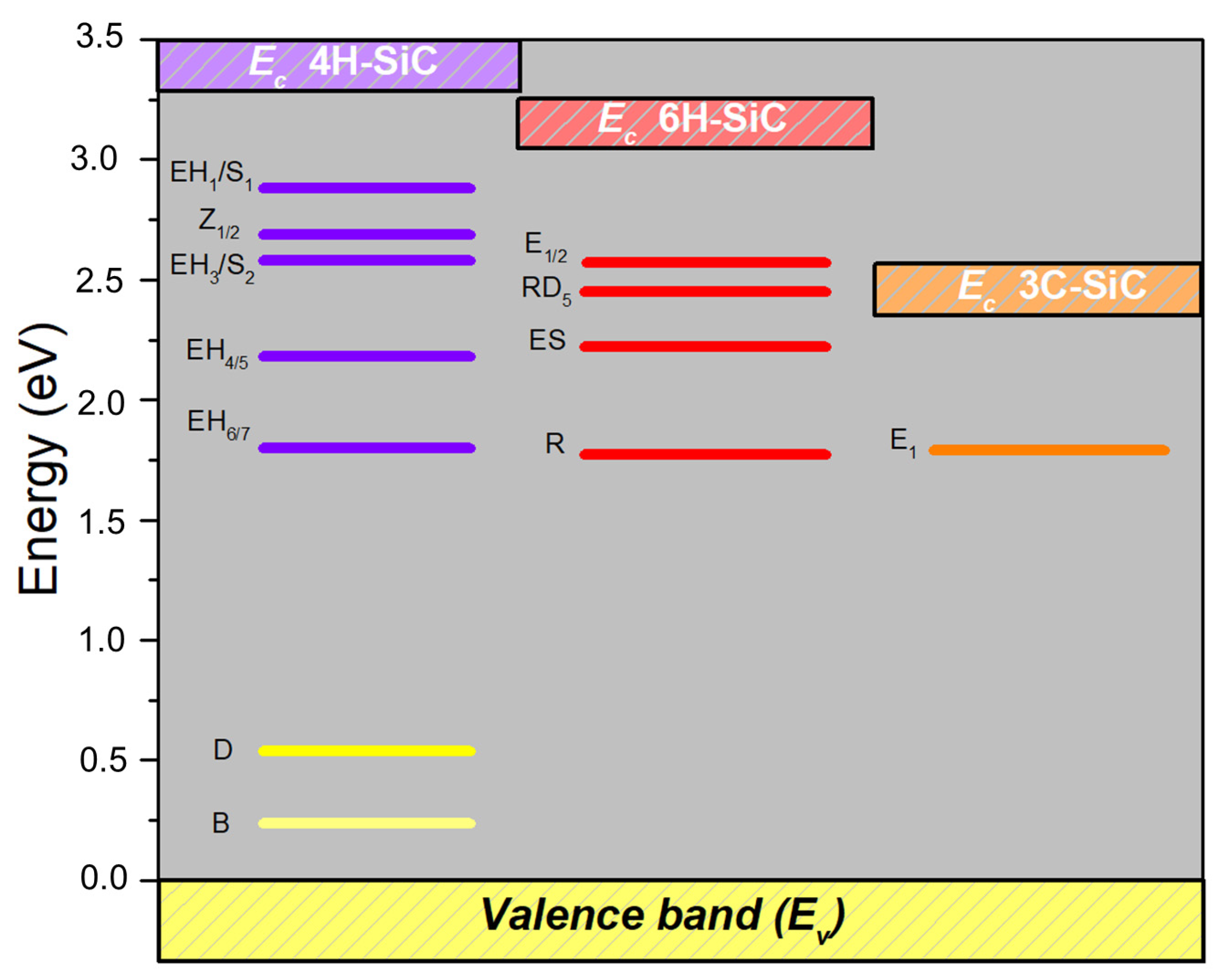
2.1. Carbon Interstitials (Ci)

The study of electrically active radiation-induced defects in 4H-SiC has been an area of significant research for many years. A wide range of such defects, introduced by various radiation sources, including protons, electrons, and neutrons, has been reported [28,29,30,31,32,33,34]. Among these, two electrically active defects with deep levels at 0.40 eV and 0.70 eV below the conduction band have garnered particular attention within the SiC research community. What makes these two defects especially intriguing is their consistent appearance together, regardless of the type of radiation source. For a long time, they remained enigmatic, and it was only recently that they were conclusively assigned to the same defect. The mystery surrounding their origin has finally been resolved. Storasta et al. [35] have used low-energy electrons to introduce only carbon displacements in the 4H-SiC lattice (C displacement threshold 20 eV, Si displacement threshold 35 eV). They observed two energy levels at EC − 0.4 eV and EC − 0.7 eV and labeled them as EH1 and EH3. These levels were assigned to a highly mobile defect, such as carbon interstitial. Alfieri et al. [36] provided compelling evidence that, under low-energy electron irradiation (E < 200 keV), only carbon interstitial-related defects are introduced, shedding light on the underlying mechanisms responsible for these two deep-level defects.
Figure 3 shows DLTS spectra for the low-energy electron (E = 150 keV) and fast neutron irradiated n-type 4H-SiC samples. In addition to Z1/2 (which will be discussed in detail later), two deep-level defects at Ec − 0.4 eV (EH1/S1) and Ec − 0.7 eV (EH3/S2) are detected in irradiated 4H-SiC samples.

2.2. Silicon Vacancy (VSi)

The S1 and S2 traps are introduced by high-energy particles such as ions, protons, and neutrons [30,33,34,37]. As seen in Figure 3, these traps exhibit the same energy levels as those of EH1 and EH3, located at EC − 0.40 eV and EC − 0.70 eV, respectively. This has caused significant confusion in distinguishing and identifying these defects over the years. Even today, when studying radiation-induced defects in SiC, it remains common practice within the research community to use the label “EH” to refer to a wide range of radiation-induced defects, further contributing to the ambiguity.
Bathen et al. [38] investigated the effects of MeV proton irradiation on 4H-SiC and observed, as expected, the two deep levels at EC − 0.40 eV and EC − 0.70 eV, designated as S1 and S2. These levels were attributed to the charge state transitions of silicon vacancies, specifically VSi(−3/=) for S1 and VSi(=/−) for S2. Using L-DLTS measurements, it was further revealed that the S1 level has two distinct emission lines corresponding to silicon vacancies located at the −k and −h lattice sites. These findings were later corroborated by Brodar et al. [39], who observed identical results when studying 4H-SiC materials irradiated with fast neutrons.
Moreover, Knežević et al. [37] have provided an additional approach to convincingly yet easily distinguish Ci and VSi. L-DLTS provides direct evidence that EH1 consists of a single emission line arising from the Ci at the −h lattice site (Figure 4a), in contrast to S1, which has two emission lines arising from the VSi at the −h and −k lattice sites (Figure 4b).
Recently, VSi defects in 4H-SiC have gained significant attention within the SiC and quantum technology communities due to their unique properties, including half-integer spin, photostability, and long spin coherence times at room temperature [5,6,7,38]. The ability to efficiently introduce and control individual VSi defects in 4H-SiC is crucial for advancing quantum technologies. Several methods have been proposed, such as irradiation, ion implantation, and laser processing [40].

2.3. Carbon Vacancy (VC)

Figure 5 shows a typical DLTS spectrum for an as-grown n-type 4H-SiC sample. Two prominent traps, Z1/2 and EH6/7, are observed. The estimated activation energies for electron emissions are 0.67 eV and 1.64 eV, respectively.
Z1/2 and EH6/7 are the most common traps in 4H-SiC, introduced either during the crystal growth or upon irradiation. The Z1/2 concentration can be further increased by irradiation or high-temperature annealing, which reduces carrier lifetime. This is the reason why Z1/2 is often called a “lifetime killer” within the SiC community [42,43,44]. However, numerous studies have shown that thermal oxidation [45] or carbon implantation followed by subsequent annealing [46,47,48] could reduce the concentration of Z1/2 and EH6/7 traps in 4H-SiC.
As shown in Figure 5, the Z1/2 introduces an asymmetric peak in the DLTS spectrum. In their pioneering work on Z1/2 using DLTS, Hemmingsson et al. [49] showed that Z1/2 is the superposition of two nearly identical Z1 and Z2 negative-U defect transitions, each located on a different sub-lattice site. Later on, by connecting electron paramagnetic resonance (EPR) and photo-EPR data with the DLTS results, it was possible to ascribe Z1/2 to transitions involving the carbon vacancy (VC) in 4H-SiC on distinct sub-lattice sites and to assign Z1/2 to a transition between double negative and neutral charge state of carbon vacancy VC (=/0) [50]. Additionally, studies using the L-DLTS technique have provided direct evidence that the Z1/2 comprises two distinct components, namely Z1 and Z2. These components were identified with activation energies for electron emission of 0.59 eV and 0.67 eV, respectively, and were attributed to the (=/0) charge transitions of VC located at −h and −k lattice sites in the 4H-SiC crystal [51,52]. Figure 6 shows L-DLTS spectra for Z1(=/0) and Z2(=/0).
Moreover, significant efforts were also undertaken to resolve the broad EH6/7 peak (Figure 4). Danno et al. [53] have successfully distinguished EH6 and EH7 through simulations of the Fourier-transform DLTS spectrum of the EH6/7 peak. Later, direct evidence that EH6/7 comprises two distinct components was provided by Alfieri et al. [54]. They have identified two separate energy levels, 1.30 eV and 1.49 eV, corresponding to EH6 and EH7, respectively.

2.4. Carbon Antisite–Carbon Vacancy (CSi-VC) Pair

The traps labeled as EH4 and EH5 are commonly observed in DLTS spectra of ion-implanted or irradiated n-type 4H-SiC samples [55,56,57]. The EH4 peak reaches its maximum at approximately 400 K (as shown in Figure 7), while the EH5 peak appears at slightly higher temperatures (not shown here). The reported activation energies for these defects are approximately 1.0–1.1 eV below the conduction band. Also, it is a practice to refer to these traps as EH4/5.
Karsthof et al. [56] have investigated the EH4 and EH5 traps using DLTS and photoluminescence (PL) in proton-irradiated and subsequently annealed n-type 4H-SiC samples. In their study, they have proposed that EH4 (EC − 1.0 eV) and EH5 (EC − 1.1 eV) arise from the (+/0) charge transition level associated with different configurations of the carbon antisite-carbon vacancy (CSi-VC) pair.
This conclusion was further validated by Nakane et al. [57], who utilized 2 MeV electron irradiation followed by annealing to introduce deep-level defects, which were analyzed using photo-induced current transient spectroscopy (PICTS) and EPR. Their study identified several deep-level defects, including two with energies of approximately 0.72 eV and 1.07 eV, which were attributed to the (0/−) and (+/0) charge transitions of the CSi-VC pair, respectively.

2.5. Boron-Related Defects

Alongside aluminum, boron is among the most widely used p-type dopants in SiC. However, its unintentional incorporation during crystal growth has been frequently reported. This phenomenon is attributed to the presence of boron impurities in the graphite susceptor used during the chemical vapor deposition (CVD) process [58,59,60,61].
Storasta et al. [62] investigated this issue by employing MCTS to examine the effects of unintentional boron incorporation in low-doped n-type 4H-SiC. The SiC samples were grown using a hot-wall CVD process. Their findings confirmed earlier reports that boron introduces two distinct deep levels, referred to as shallow boron (B) and deep boron (D-center). Figure 8 shows MCTS spectra for as-grown and neutron irradiated n-type 4H-SiC samples: (a) shallow boron, B and (b) deep boron, D-center. The activation energies for hole emissions for B and D-center are estimated as EV + 0.28 eV and EV + 0.61 eV, respectively [34,62,63,64,65].
Bockstedte et al. [65] further identified the origin of these boron-related levels. The shallow boron level (B) was attributed to boron atoms substituting silicon atoms (BSi) in an off-center configuration. The D-center, associated with deep boron, was assigned to boron atoms substituting carbon atoms (BC) in a perfect substitutional configuration. This defect was initially observed to create a deep level at ~0.60 eV above the valence band based on DLTS measurements. However, recent L-DLTS studies revealed that the D-center consists of two emission lines with activation energies of EV + 0.49 eV and EV + 0.57 eV [34]. These levels are associated with boron atoms occupying −h and −k lattice sites, respectively. Although VC has been identified as the dominant carrier lifetime limiting defect in 4H-SiC, Ghezellou et al. [64] have reported an extensive study on boron-related defects being another dominant source of recombination and acting as lifetime limiting defects in 4H–SiC material. They have reported a minority carrier lifetime of up to 2.5 µs. The improvement of minority carrier lifetime in 4H-SiC is crucial for bipolar devices.
In this section, we have provided an overview of the most significant electrically active defects in 4H-SiC. These defects can either be intrinsic, present in as-grown material, or induced by various radiation sources, such as electrons, protons, ions, and neutrons. Table 2 summarizes the information on the most important defects in 4H-SiC.
It is important to note that the electrically active defects discussed here do not represent an exhaustive list. Other defects, including those associated with impurities such as nitrogen [66] and vanadium [67], have also been observed in 4H-SiC. However, we have deliberately chosen not to include them in this discussion. The primary objective of this review is to maintain a focused and structured approach, making it easier to follow, rather than attempting to provide an exhaustive survey of all reported defects in the literature.
By narrowing our focus, we aim to highlight the most relevant defects in the context of their impact on the electrical properties of 4H-SiC, particularly those that are crucial for its applications in power electronics, quantum technologies, and radiation detection. Future studies may expand upon this foundation by incorporating a broader range of defect types, including impurity-related and process-induced defects.

3. 6H-SiC

6H-SiC is distinguished by its wide bandgap (3.02 eV), high thermal conductivity, and exceptional robustness under extreme conditions, making it a highly versatile material for applications in high-temperature electronics, radiation-hardened devices, and optoelectronics. However, despite these advantages, its lower electron mobility compared to 4H-SiC (as shown in Table 1) limits its suitability for power electronic applications, where high carrier mobility is essential for achieving efficient performance. This limitation has resulted in a significantly lower number of published studies on intrinsic or radiation-induced defects in 6H-SiC compared to 4H-SiC, which remains the preferred polytype for most power and high-frequency applications. In this section, we provide an overview of the most significant achievements in the study of electrically active defects in 6H-SiC.

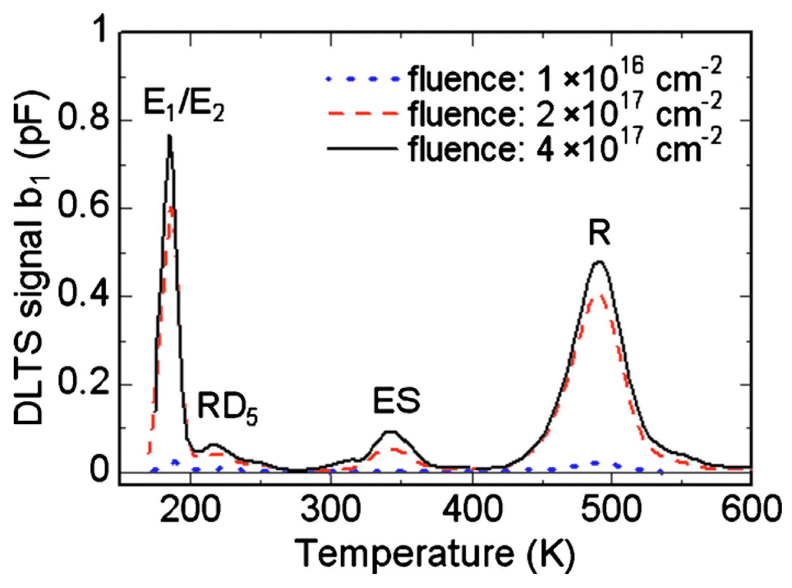
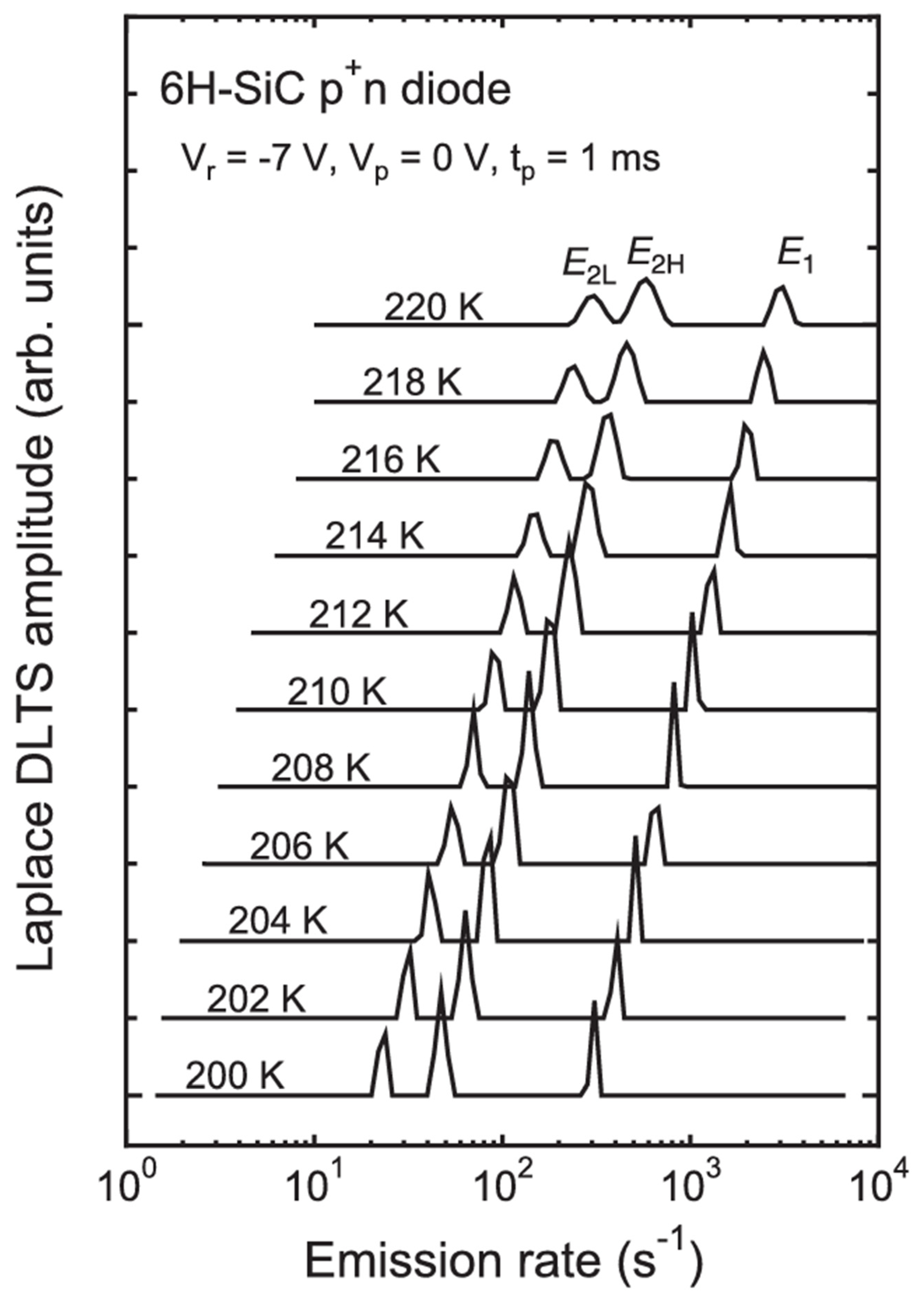
3.1. Carbon Vacancy (VC)

Figure 9 shows DLTS spectra of as-irradiated n-type 6H-SiC. The low-energy electron irradiation (E = 150 keV) with fluencies 1 × 10¹⁶, 2 × 10¹⁶, and 4 × 1017 cm−2 was used [68]. It should be noted that E1/2 (0.45 eV) and R (1.25 eV) traps were already present in the DLTS spectrum for as-grown 6H-SiC materials, while RD5 (0.57 eV) and ES (0.80 eV) traps are observed only after low-energy electron irradiation.
Based on defect generation rates and annealing behavior, Sasaki et al. [68] proposed that E1/2 and R in n-type 6H-SiC correspond to Z1/2 and EH6/7 in n-type 4H-SiC (Section 2) and are attributed to the carbon vacancy (VC). Similar to the Z1/2 in 4H-SiC, the E1/2 trap in 6H-SiC has attracted significant research attention. Initially, the E1/2 DLTS peak was separated into two components, leading to the interpretation that E1 and E2 correspond to VC at two distinct lattice sites, −h and −k. However, this interpretation was challenged by Pensl et al. [69], who correctly pointed out that 6H-SiC has three non-equivalent lattice sites for vacancies: one hexagonal (−h) and two cubic (−k1 and −k2). Their analysis suggested that a three-component structure was more likely, rather than just two. Building upon this hypothesis, Koizumi et al. [70] successfully resolved the E1/2 into three distinct emission components using L-DLTS. As illustrated in Figure 10, their results confirm that E1/2 consists of three individual peaks (labeled as E2L, E2H, and E1), corresponding to the acceptor levels of carbon vacancies at the three non-equivalent lattice sites in 6H-SiC. This finding represents a major advancement in the understanding of VC defects in 6H-SiC, offering greater insight into their electronic properties.

3.2. Carbon Interstitials (Ci)

As already mentioned, RD5 and ES traps (shown in Figure 9) are not observed in as-grown 6H-SiC material, but they only appear upon irradiation. Sasaki et al. [68] investigated the annealing behavior of these defects, and their findings indicate that both RD5 and ES are thermally unstable. Interestingly, the similarities between the RD5 and ES traps in n-type 6H-SiC and the EH1 and EH3 traps in n-type 4H-SiC are striking, naturally leading to the assumption that they originate from the same underlying defects. These similarities include (i) the fact that all these traps are induced by low-energy electron irradiation (E < 200 keV) and (ii) they anneal out at relatively low temperatures. Based on experimental and theoretical evidence, Sasaki et al. [68] have proposed that RD5 and ES are associated with carbon interstitials (Ci).
Additionally, a broad peak appearing at a similar temperature position as ES has been observed and labeled as Z1/2 [71]. This designation can be misleading, as Z1/2 in 6H-SiC has no connection whatsoever with Z1/2 in 4H-SiC. The Z1/2 trap is observed in n-type 6H-SiC upon 2.5 MeV He+ ion implantation [71]. The activation energy for electron emission of Z1/2 (0.71 eV) is close to the activation energy of ES (0.80 eV), but there is no conclusive evidence proving that these traps originate from the same defect. Ruggiero et al. [71] attributed the Z1/2 trap to the divacancy (VC-VSi) based on DLTS and photoluminescence (PL) measurements. Applying a comparative approach with 4H-SiC, where traps (S1/2) are introduced by high-energy particles such as protons or ions have been identified as silicon vacancy (VSi), it is reasonable to assume that the Z1/2 trap is indeed related to divacancies rather than carbon interstitials. Table 3 provides a summary of the most common defects in 6H-SiC.

3.3. Applications

As discussed in Section 2, point defects such as the silicon vacancy (VSi) have shown great promise for quantum technology applications and have been extensively studied in 4H-SiC [5,6,7,38,40]. These defects exhibit long spin coherence times and optically addressable spin states, making them highly relevant for quantum computing, sensing, and communication.
However, the physics of similar defects in other SiC polytypes remains significantly less explored. Understanding their properties across different polytypes is crucial, as variations in stacking order and crystal symmetry can strongly influence defect formation, charge states, and optical transitions.
Recently, Ousdai et al. [72] investigated the formation and thermal stability of point defects in 6H-SiC using PL spectroscopy. Their findings are promising, revealing defect-related emissions that suggest 6H-SiC could also be a viable platform for quantum applications. These results open up a new research direction, highlighting the potential of 6H-SiC for quantum technologies and warranting further studies to explore its suitability in areas such as spin qubits and single-photon emission.
Future investigations will be essential to fully characterize the quantum coherence properties of defects in 6H-SiC and compare their performance with those in 4H-SiC. If successful, this could broaden the scope of SiC-based quantum devices and expand the material choices available for next-generation quantum technologies.
It is worth mentioning that 6H-SiC has already found its place in several niche applications. Thanks to its high crystalline quality, 6H-SiC is used as a substrate for growing epitaxial layers of 4H-SiC or GaN [73,74]. Additionally, 6H-SiC polytype has been proposed for UV and visible light devices [75].

4. 3C-SiC

For many years, the 3C-SiC polytype has been proposed as the most promising SiC polytype for electronic device applications due to its unique advantages. These advantages include lower production costs than 4H-SiC and, most importantly, its ability to be grown epitaxially on large-area, cost-effective silicon (Si) wafers. This compatibility with existing Si-based semiconductor technology facilitates easier integration into established manufacturing processes [76]. However, this compatibility did not come without the price. The mismatch in the lattice constant and thermal expansion coefficient between 3C-SiC and Si can introduce electrically active defects [77]. Moreover, 3C-SiC possesses a lower bandgap of 2.36 eV compared to 4H-SiC (3.26 eV) and 6H-SiC (3.02 eV). This fact limits its performance in high-power and high-temperature devices where wider bandgaps are advantageous.

4.1. Electrically Active Defects

The number of available studies on 3C-SiC is significantly lower compared to its 4H- and 6H-SiC counterparts (Figure 2). In the early investigations of defects in 3C-SiC, a variety of deep-level defects were reported. However, it was initially unclear whether these defects originated from the growth process, were related to the Si/3C-SiC interface, or were intrinsic to 3C-SiC itself. A pioneering effort in this field was led by M. Kato [77,78,79], who systematically examined defects in 3C-SiC and identified several traps arising from the 3C-SiC/Si interface. This work provided crucial insights into distinguishing interface-related states from bulk defects in 3C-SiC. Later studies expanded on this foundation by investigating both as-grown and radiation-induced defects in 3C-SiC.
Nagesh et al. [76] investigated neutron-irradiated n-type and p-type 3C-SiC. In n-type material, they observed an electron trap located at EC − 0.49 eV, while in p-type material, they identified three hole traps at EV + 0.18 eV, EV + 0.24 eV, and EV + 0.51 eV. These findings highlight the impact of neutron irradiation on carrier trapping and recombination processes in 3C-SiC. Weidner et al. [80] investigated intrinsic defects introduced in n-type 3C-SiC by H+ and He implantation, as well as high-energy electron irradiation. They reported the presence of nine distinct deep-level defects labeled W1-W9. Among these, the W6 trap, with an activation energy for electron emission of 0.58 eV, was the most dominant. Remarkably, W6 showed strong similarities to the Z1/2 trap in 4H-SiC, which has been attributed to the carbon vacancy (VC). Further investigations by Beyer et al. [81] provided additional confirmation that the E1 trap (0.57 eV) observed in their study of n-type 3C-SiC corresponds to the W6 trap described by Weidner et al. [82], and they assigned it to the carbon vacancy in 3C-SiC. This identification is a crucial step toward understanding the role of vacancy-related defects in 3C-SiC, as VC plays a pivotal role in carrier recombination. The carbon vacancy’s significance extends across all SiC polytypes, and it is the only defect that has been extensively studied and convincingly confirmed in 3C, 4H, and 6H-SiC polytypes.

4.2. Applications

With its cubic structure and inherent compatibility with existing silicon technology, 3C-SiC presents unique opportunities for niche applications that leverage its exceptional material properties. While it has not yet reached the same level of industrial maturity as 4H-SiC, ongoing research continues to highlight its potential in several key areas. These applications include, but are not limited to:
(i)
Solar Cells:
3C-SiC’s excellent thermal stability and a bandgap wider than Si (1.12eV) make it a strong candidate for next-generation solar cells. Unlike traditional silicon-based solar cells, 3C-SiC can operate efficiently in extreme environments, including high radiation and high temperatures [82,83,84].
(ii)
Quantum applications:
Similar to its 4H and 6H counterparts, the potential of 3C-SiC for quantum qubits and quantum sensing has gained attention [85,86,87]. However, as is the case with other SiC polytypes, the primary challenge remains defect engineering. This involves the precise introduction and control of individual defect centers, which is crucial for harnessing the material’s full capabilities in quantum applications.
(iii)
Biomedical Devices and Bioelectronics:
One of the most promising application areas for 3C-SiC is for biomedical devices and bioelectronics [88]. 3C-SiC is recognized as a bio- and hemo-compatible material, meaning it does not induce immune responses or blood clotting upon contact with biological tissues [89]. These properties make it highly suitable for implantable medical devices and biosensors [90,91].
In summary, the characterization of electrically active defects in 3C-SiC remains an open field of research. Compared to 4H-SiC, where defect identification has reached a mature stage (at least for n-type material), many questions regarding the nature, stability, and impact of electrically active defects in 3C-SiC are still open. Further investigations combining DLTS with complementary spectroscopic techniques such as EPR and PL are necessary to provide a more comprehensive understanding of defect physics in 3C-SiC and its impact on electronic and optoelectronic device applications.

5. Conclusions

Figure 11 shows a diagram with the most common electrically active defects in 3C-SiC, 4H-SiC, and 6H-SiC. As highlighted from the outset and further emphasized in Figure 1, there is a significant discrepancy in the number of published studies focusing on these polytypes. Specifically, while defect-related research on 4H-SiC has been extensive and comprehensive over the years, studies on 3C-SiC and 6H-SiC remain relatively limited.
Due to the sheer volume of research, we can confidently state that most aspects of the defect landscape in 4H-SiC have been well-characterized, with many pieces of the puzzle now fitting into place. Ghezellou et al. [92] have recently made additional progress in understanding the influence of 4H-SiC epitaxial growth conditions with defect concentration and minority carrier lifetime. They have observed that the choice of hydrocarbon plays a crucial role in nitrogen doping incorporation, particularly at lower N/C ratios. This variation is likely due to differences in the surface diffusivity of species from each hydrocarbon, affecting the site-competition mechanism during nitrogen incorporation at lower doping levels. Additionally, this study indicates a significant difference in minority carrier lifetime between the different hydrocarbons (minority carrier lifetime up to 1.1 µs). Also, different hydrocarbons affect the carbon vacancy concentration.
Moreover, it is evident that 4H-SiC has become the dominant polytype in power electronics, where it serves as the key material driving advancements in high-performance semiconductor devices. Additionally, 4H-SiC is steadily gaining recognition as a promising candidate for emerging applications in quantum technologies and radiation detection. In recent years, significant progress in that direction has been achieved by deep-learning methods. Kobayashi et al. [93] have used a physics-regularized neural network as a computational approach to predict silicon carbide’s swelling under high-irradiation conditions, which are essential for nuclear and aerospace applications. Liao et al. [94] have applied deep-learning-enhanced methods to extract parameters of single-spin readout in SiC, which is crucial for quantum application.
In contrast to 4H, the understanding of defects in 3C-SiC and 6H-SiC is still evolving, with significant gaps that require further investigation. 3C-SiC and 6H-SiC have not yet reached the same level of technological maturity, limiting the full exploration of their potential applications. In this review paper, we have addressed specific aspects of defect-related challenges in 3C-SiC and 6H-SiC, shedding light on niche areas that warrant further attention. However, as research efforts on these polytypes continue to expand in the future, the scope of the investigation will undoubtedly broaden, revealing new applications.

Funding

This research received no external funding.

Data Availability Statement

Data are contained within the article.

Acknowledgments

The author would like to thank Ivana Panžić and Ivan Capan for their useful comments on the manuscript.

Conflicts of Interest

The author declares no conflicts of interest.

Abbreviations

DLTSdeep-level transient spectroscopy
L-DLTSLaplace deep-level transient spectroscopy
MCTSminority carrier transient spectroscopy
PLphotoluminescence
EPRelectron paramagnetic resonance
MOSFETmetal-oxide-semiconductor field-effect transistor
CVDchemical vapor deposition

References

  1. Kimoto, T.; Cooper, J.A. Fundamentals of Silicon Carbide Technology: Growth, Characterization, Devices, and Applications; John Wiley & Sons Singapore Pte. Ltd.: Hoboken, NJ, USA, 2014. [Google Scholar]
  2. Matsunami, H. Fundamental research on semiconductor SiC and its applications to power electronics. Proc. Jpn. Acad. Ser. B Phys. Biol. Sci. 2020, 96, 235–254. [Google Scholar] [CrossRef] [PubMed]
  3. Hedayati, R.; Lanni, L.; Rodriguez, S.; Malm, B.G.; Rusu, A.; Zetterling, C.M. A monolithic, 500 °C operational amplifier in 4H-SiC bipolar technology. IEEE Electron. Device Lett. 2014, 35, 693–695. [Google Scholar] [CrossRef]
  4. Ryu, S.-H.; Krishnaswami, S.; Hull, B.; Heath, B.; Das, M.; Richmond, J.; Fatima, H.; Zhang, J.; Agarwal, A.; Palmour, J.; et al. High Speed Switching Devices in 4H-SiC—Performance and Reliability. In Proceedings of the 2005 IEEE International Semiconductor Device Research Symposium, Bethesda, MD, USA, 7–9 December 2005; pp. 162–163. [Google Scholar]
  5. Wang, J.; Zhou, Y.; Zhang, X.; Liu, F.; Li, Y.; Li, K.; Liu, Z.; Wang, G.; Gao, W. Efficient Generation of an Array of Single Silicon-Vacancy Defects in Silicon Carbide. Phys. Rev. Appl. 2017, 7, 064021. [Google Scholar] [CrossRef]
  6. Widmann, M.; Lee, S.Y.; Rendler, T.; Son, N.T.; Fedder, H.; Paik, S.; Yang, L.P.; Zhao, N.; Yang, S.; Booker, I.; et al. Coherent control of single spins in silicon carbide at room temperature. Nat. Mater. 2015, 14, 164–168. [Google Scholar] [CrossRef] [PubMed]
  7. Fuchs, F.; Stender, B.; Trupke, M.; Simin, D.; Pflaum, J.; Dyakonov, V.; Astakhov, G.V. Engineering near-infrared single-photon emitters with optically active spins in ultrapure silicon carbide. Nat. Commun. 2015, 6, 7578. [Google Scholar] [CrossRef]
  8. Radulović, V.; Yamazaki, Y.; Pastuović, Ž.; Sarbutt, A.; Ambrožič, K.; Bernat, R.; Ereš, Z.; Coutinho, J.; Ohshima, T.; Capan, I.; et al. Silicon carbide neutron detector testing at the JSI TRIGA reactor for enhanced border and port security. Nucl. Instrum. Methods Phys. Res. Sect. A Accel. Spectrometers Detect. Assoc. Equip. 2020, 972, 164122. [Google Scholar] [CrossRef]
  9. Ruddy, F.H.; Seidel, J.G.; Chen, H.; Dulloo, A.R.; Ryu, S.H. High-resolution alpha-particle spectrometry using silicon carbide semiconductor detectors. IEEE Nucl. Sci. Symp. Conf. Rec. 2005, 3, 1231–1235. [Google Scholar]
  10. Zaťko, B.; Hrubčín, L.; Šagátová, A.; Osvald, J.; Boháček, P.; Kováčová, E.; Halahovets, Y.; Rozov, S.V.; Sandukovskij, V.G. Study of Schottky barrier detectors based on a high quality 4H-SiC epitaxial layer with different thickness. Appl. Surf. Sci. 2021, 536, 147801. [Google Scholar] [CrossRef]
  11. Kleppinger, J.W.; Chaudhuri, S.K.; Karadavut, O.F.; Mandal, K. C Defect characterization and charge transport measurements in high-resolution Ni/n-4H-SiC Schottky barrier radiation detectors fabricated on 250 μm epitaxial layers. J. Appl. Phys. 2021, 129, 244501. [Google Scholar] [CrossRef]
  12. Bernat, R.; Capan, I.; Bakrač, L.; Brodar, T.; Makino, T.; Ohshima, T.; Pastuović, Ž.; Sarbutt, A. Response of 4h-sic detectors to ionizing particles. Crystals 2021, 11, 10. [Google Scholar] [CrossRef]
  13. Flammang, R.W.; Seidel, J.G.; Ruddy, F.H. Fast neutron detection with silicon carbide semiconductor radiation detectors. Nucl. Instrum. Methods Phys. Res. Sect. A Accel. Spectrometers Detect. Assoc. Equip. 2007, 579, 177–179. [Google Scholar] [CrossRef]
  14. Capan, I. 4H-SiC Schottky Barrier Diodes as Radiation Detectors: A Review. Electronics 2022, 11, 532. [Google Scholar] [CrossRef]
  15. Coutinho, J.; Torres, V.J.B.; Capan, I.; Brodar, T.; Ereš, Z.; Bernat, R.; Radulović, V. Silicon carbide diodes for neutron detection. Nucl. Inst. Methods Phys. Res. A 2020, 986, 164793. [Google Scholar] [CrossRef]
  16. Langpoklakpam, C.; Liu, A.-C.; Chu, K.-H.; Hsu, L.-H.; Lee, W.-C.; Chen, S.-C.; Sun, C.-W.; Shih, M.-H.; Lee, K.-Y.; Kuo, H.-C. Review of Silicon Carbide Processing for Power MOSFET. Crystals 2022, 12, 245. [Google Scholar] [CrossRef]
  17. Dalibor, T.; Pensl, G.; Matsunami, H.; Kimoto, T.; Choyke, W.J.; Schöner, A.; Nordell, N. Deep Defect Centers in Silicon Carbide Monitored with Deep Level Transient Spectroscopy. Phys. Status Solidi A 1997, 162, 199–225. [Google Scholar] [CrossRef]
  18. Taha, W. Comparative Study on Silicon Carbide (SiC) Polytypes in High Voltage Devices. In Proceedings of the 2021 International Conference on Sustainable Energy and Future Electric Transportation (SEFET), Hyderabad, India, 21–23 January 2021; pp. 1–6. [Google Scholar]
  19. Rodrigues, C.G. Electron Mobility in Bulk n-Doped SiC-Polytypes 3C-SiC, 4H-SiC, and 6H-SiC: A Comparison. Semiconductors 2021, 55, 625–632. [Google Scholar] [CrossRef]
  20. Mekaret, F.; Rabehi, A.; Zebentout, B.; Tizi, S.; Douara, A.; Bellucci, S.; Guermoui, M.; Benamara, Z.; El-Kenawy, E.-S.M.; Eid, M.M.; et al. A Comparative Study of Schottky Barrier Heights and Charge Transport Mechanisms in 3C, 4H, and 6H Silicon Carbide Polytypes. AIP Adv. 2024, 14, 115302. [Google Scholar] [CrossRef]
  21. Bhatnagar, M.; Baliga, B.J. Comparison of 6H-SiC, 3C-SiC, and Si for Power Devices. IEEE Trans. Electron Devices 1993, 40, 645–655. [Google Scholar] [CrossRef]
  22. Capan, I.; Brodar, T. Majority and Minority Charge Carrier Traps in n-Type 4H-SiC Studied by Junction Spectroscopy Techniques. Electron. Mater. 2022, 3, 115–123. [Google Scholar] [CrossRef]
  23. Peaker, A.R.; Dobachewski, L. Laplace-transform deep-level spectroscopy: The technique and its applications to the study of point defects in semiconductors. J. Appl. Phys. 2004, 96, 4689. [Google Scholar]
  24. Hamilton, B.; Peaker, A.R.; Wight, D.R. Deep-state-controlled minority-carrier lifetime in n-type gallium phosphide. J. Appl. Phys. 1979, 50, 6373–6385. [Google Scholar] [CrossRef]
  25. Brunwin, R.; Hamilton, B.; Jordan, P.; Peaker, A.R. Detection of minority-carrier traps using transient spectroscopy. Electron. Lett. 1979, 15, 349–350. [Google Scholar] [CrossRef]
  26. Huang, Y.; Wang, R.; Zhang, Y.; Yang, D.; Pi, X. Compensation of p-Type Doping in Al-Doped 4H-SiC. J. Appl. Phys. 2022, 131, 185703. [Google Scholar] [CrossRef]
  27. Nguyen, T.-K.; Phan, H.-P.; Dinh, T.; Toriyama, T.; Nakamura, K.; Foisal, A.R.M.; Nguyen, N.-T.; Dao, D.V. Isotropic Piezoresistance of p-Type 4H-SiC in (0001) Plane. Appl. Phys. Lett. 2018, 113, 012104. [Google Scholar] [CrossRef]
  28. Paradzah, A.T.; Auret, F.D.; Legodi, M.J.; Omotoso, E.; Diale, M. Electrical characterization of 5.4 MeV alpha-particle irradiated 4H-SiC with low doping density. Nucl. Instrum. Methods Phys. Res. Sect. B Beam Interact. Mater. Atoms. 2015, 358, 112–116. [Google Scholar] [CrossRef]
  29. Omotoso, E.; Meyer, W.E.; Auret, F.D.; Paradzah, A.T.; Legodi, M.J. Electrical characterization of deep levels created by bombarding nitrogen-doped 4H-SiC with alpha-particle irradiation. Nucl. Instrum. Methods Phys. Res. Sect. B Beam Interact. Mater. Atoms. 2016, 371, 312–316. [Google Scholar] [CrossRef]
  30. David, M.L.; Alfieri, G.; Monakhov, E.M.; Hallén, A.; Blanchard, C.; Svensson, B.G.; Barbot, J.F. Electrically active defects in irradiated 4H-SiC. J. Appl. Phys. 2004, 95, 4728–4733. [Google Scholar] [CrossRef]
  31. Alfieri, G.; Monakhov, E.V.; Svensson, B.G.; Linnarsson, M.K. Annealing behavior between room temperature and 2000 °C of deep level defects in electron-irradiated n-type 4H silicon carbide. J. Appl. Phys. 2005, 98, 043518. [Google Scholar] [CrossRef]
  32. Iwamoto, N.; Johnson, B.C.; Hoshino, N.; Ito, M.; Tsuchida, H.; Kojima, K.; Ohshima, T. Defect-induced performance degradation of 4H-SiC Schottky barrier diode particle detectors. J. Appl. Phys. 2013, 113, 143714. [Google Scholar] [CrossRef]
  33. Pastuović, Z.; Siegele, R.; Capan, I.; Brodar, I.; Sato, S.; Ohshima, T. Deep level defects in 4H-SiC introduced by ion implantation: The role of single ion regime. J. Phys. Condens. Matter 2017, 29, 475701. [Google Scholar] [CrossRef]
  34. Capan, I.; Brodar, T.; Yamazaki, Y.; Oki, Y.; Ohshima, T.; Chiba, Y.; Hijikata, Y.; Snoj, L.; Radulović, V. Influence of neutron radiation on majority and minority carrier traps in n-type 4H-SiC. Nucl. Instrum. Methods Phys. Res. Sect. B Beam Interact. Mater. Atoms. 2020, 478, 224–228. [Google Scholar] [CrossRef]
  35. Storasta, L.; Bergman, J.P.; Janzén, E.; Henry, A.; Lu, J. Deep levels created by low energy electron irradiation in 4H-SiC. J. Appl. Phys. 2004, 96, 4909–4915. [Google Scholar] [CrossRef]
  36. Alfieri, G.; Mihaila, A. Isothermal annealing study of the EH1 and EH3 levels in n-type 4H-SiC. J. Phys. Condens. Matter 2020, 32, 46. [Google Scholar] [CrossRef] [PubMed]
  37. Knežević, T.; Brodar, T.; Radulović, V.; Snoj, L.; Makino, T.; Capan, I. Distinguishing the EH1 and S1 defects in n-type 4H-SiC by Laplace DLTS. Appl. Phys. Express 2022, 15, 101002. [Google Scholar] [CrossRef]
  38. Bathen, M.E.; Galeckas, A.; Müting, J.; Ayedh, H.M.; Grossner, U.; Coutinho, J.; Frodason, Y.K.; Vines, L. Electrical charge state identification and control for the silicon vacancy in 4H-SiC. NPJ Quantum Inf. 2019, 5, 111. [Google Scholar] [CrossRef]
  39. Brodar, T.; Capan, I.; Radulović, V.; Snoj, L.; Pastuović, Z.; Coutinho, J.; Ohshima, T. Laplace DLTS study of deep defects created in neutron-irradiated n-type 4H-SiC. Nucl. Instrum. Methods Phys. Res. Sect. B Beam Interact. Mater. Atoms. 2018, 437, 27–31. [Google Scholar] [CrossRef]
  40. Nagy, R.; Widmann, M.; Niethammer, M.; Dasari, D.B.R.; Gerhardt, I.; Soykal, Ö.O.; Radulaski, M.; Ohshima, T.; Vučić, J.; Son, N.T.; et al. Quantum Properties of Dichroic Silicon Vacancies in Silicon Carbide. Phys. Rev. Appl. 2018, 9, 034022. [Google Scholar] [CrossRef]
  41. Capan, I. An Overview of Radiation Induced Deep Level Defects in n-type 4H-SiC Studied by Junction Spectroscopy Techniques. Preprints 2022, 2022010360. [Google Scholar] [CrossRef]
  42. Kimoto, T.; Danno, K.; Suda, J. Lifetime-killing defects in 4H-SiC epilayers and lifetime control by low-energy electron irradiation. Phys. Status Solidi 2008, 245, 1327–1336. [Google Scholar] [CrossRef]
  43. Hazdra, P.; Popelka, S.; Schöner, A. Local Lifetime Control in 4H-SiC by Proton Irradiation. Mater. Sci. Forum 2018, 924, 436–439. [Google Scholar] [CrossRef]
  44. Galeckas, A.; Ayedh, H.M.; Bergman, J.P.; Svensson, B.G. Depth-Resolved Carrier Lifetime Measurements in 4H-SiC Epilayers Monitoring Carbon Vacancy Elimination. Mater. Sci. Forum 2017, 897, 258–261. [Google Scholar] [CrossRef]
  45. Saito, E.; Suda, J.; Kimoto, T. Control of carrier lifetime of thick n-type 4H-SiC epilayers by high-temperature Ar annealing. Appl. Phys. Express 2016, 9, 061303. [Google Scholar] [CrossRef]
  46. Miyazawa, T.; Tsuchida, H. Point defect reduction and carrier lifetime improvement of Si- and C-face 4H-SiC epilayers. J. Appl. Phys. 2013, 113, 083714. [Google Scholar] [CrossRef]
  47. Storasta, L.; Tsuchida, H. Reduction of Traps and Improvement of Carrier Lifetime in SiC Epilayer by Ion Implantation. Mater. Sci. Forum 2007, 556–557, 603–606. [Google Scholar] [CrossRef]
  48. Kushibe, M.; Nishio, J.; Iijima, R.; Miyasaka, A.; Asamizu, H.; Kitai, H.; Kosugi, R.; Harada, S.; Kojima, K. Carrier Lifetimes in 4H-SiC Epitaxial Layers on the C-Face Enhanced by Carbon Implantation. Mater. Sci. Forum 2018, 924, 432–435. [Google Scholar] [CrossRef]
  49. Hemmingsson, C.G.; Son, N.T.; Ellison, A.; Zhang, J.; Janzén, E. Negative- U centers in 4 H silicon carbide. Phys. Rev. B 1998, 58, R10119–R10122. [Google Scholar] [CrossRef]
  50. Son, N.T.; Trinh, X.T.; Løvlie, L.S.; Svensson, B.G.; Kawahara, K.; Suda, J.; Kimoto, T.; Umeda, T.; Isoya, J.; Makino, T.; et al. Negative-U System of Carbon Vacancy in 4H-SiC. Phys. Rev. Lett. 2012, 109, 187603. [Google Scholar] [CrossRef]
  51. Capan, I.; Brodar, T.; Pastuović, Z.; Siegele, R.; Ohshima, T.; Sato, S.I.; Makino, T.; Snoj, L.; Radulović, V.; Coutinho, J.; et al. Double negatively charged carbon vacancy at the h- and k-sites in 4H-SiC: Combined Laplace-DLTS and DFT study. J. Appl. Phys. 2018, 123, 161597. [Google Scholar] [CrossRef]
  52. Capan, I.; Brodar, T.; Coutinho, J.; Ohshima, T.; Markevich, V.P.; Peaker, A.R. Acceptor levels of the carbon vacancy in 4 H-SiC: Combining Laplace deep level transient spectroscopy with density functional modeling. J. Appl. Phys. 2018, 124, 245701. [Google Scholar] [CrossRef]
  53. Danno, K.; Kimoto, T. Investigation of Deep Levels in n-Type 4H-SiC Epilayers Irradiated with Low-Energy Electrons. J. Appl. Phys. 2006, 100, 113728. [Google Scholar] [CrossRef]
  54. Alfieri, G.; Kimoto, T. Resolving the EH6/7 level in 4H-SiC by Laplace-transform deep level transient spectroscopy. Appl. Phys. Lett. 2013, 102, 152108. [Google Scholar] [CrossRef]
  55. Capan, I.; Brodar, T.; Makino, T.; Radulovic, V.; Snoj, L. M-Center in Neutron-Irradiated 4H-SiC. Crystals 2021, 11, 1404. [Google Scholar] [CrossRef]
  56. Karsthof, R.; Bathen, M.E.; Galeckas, A.; Vines, L. Conversion pathways of primary defects by annealing in proton-irradiated n-type 4H-SiC. Phys. Rev. B 2020, 102, 184111. [Google Scholar] [CrossRef]
  57. Nakane, H.; Kato, M.; Ohkouchi, Y.; Trinh, X.T.; Ivanov, I.G.; Ohshima, T.; Son, N.T. Deep levels related to the carbon antisite–vacancy pair in 4H-SiC. J. Appl. Phys. 2021, 130, 065703. [Google Scholar] [CrossRef]
  58. Beyer, F.C.; Hemmingsson, C.G.; Leone, S.; Lin, Y.-C.; Gällström, A.; Henry, A.; Janzén, E. Deep levels in iron doped n- and p-type 4H-SiC. J. Appl. Phys. 2011, 110, 123701. [Google Scholar] [CrossRef]
  59. Zhang, J.; Storasta, L.; Bergman, J.P.; Son, N.T.; Janzén, E. Electrically active defects in n-type 4H-silicon carbide grown in a vertical hot-wall reactor. J. Appl. Phys. 2003, 93, 4708–4714. [Google Scholar] [CrossRef]
  60. Yang, A.; Murata, K.; Miyazawa, T.; Tawara, T.; Tsuchida, H. Analysis of carrier lifetimes in N + B-doped n-type 4H-SiC epilayers. J. Appl. Phys. 2019, 126, 055103. [Google Scholar] [CrossRef]
  61. Knezevic, T.; Jelavić, E.; Yamazaki, Y.; Ohshima, T.; Makino, T.; Capan, I. Boron-Related Defects in N-Type 4H-SiC Schottky Barrier Diodes. Materials 2023, 16, 3347. [Google Scholar] [CrossRef]
  62. Storasta, L.; Bergman, J.P.; Hallin, C.; Janzen, E. Electrical Activity of Residual Boron in Silicon Carbide. Mater. Sci. Forum 2002, 389–393, 549–552. [Google Scholar] [CrossRef]
  63. Für, N.; Belanche, M.; Martinella, C.; Kumar, P.; Bathen, M.E.; Grossner, U. Investigation of electrically active defects in SiC power diodes caused by heavy ion irradiation. IEEE Trans. Nucl. Sci. 2023, 70, 1892–1899. [Google Scholar] [CrossRef]
  64. Ghezellou, M.; Kumar, P.; Bathen, M.E.; Karsthof, R.; Sveinbjörnsson, E.Ö.; Grossner, U.; Bergman, J.P.; Vines, L.; Ul-Hassan, J. The role of boron related defects in limiting charge carrier lifetime in 4H-SiC epitaxial layers. APL Mater. 2023, 11, 031107. [Google Scholar] [CrossRef]
  65. Bockstedte, M.; Mattausch, A.; Pankratov, O. Boron in SiC: Structure and kinetics. Mater. Sci. Forum 2001, 353–356, 447. [Google Scholar] [CrossRef]
  66. Gelczuk, Ł.; Dąbrowska-Szata, M.; Kolkovsky, V.; Sochacki, M.; Szmidt, J.; Gotszalk, T. Origin and Anomalous Behavior of Dominant Defects in 4H-SiC Studied by Conventional and Laplace Deep Level Transient Spectroscopy. J. Appl. Phys. 2020, 127, 064503. [Google Scholar] [CrossRef]
  67. Lauer, V.; Brémond, G.; Souifi, A.; Guillot, G.; Chourou, K.; Anikin, M.; Madar, R.; Clerjaud, B.; Naud, C. Electrical and Optical Characterisation of Vanadium in 4H- and 6H-SiC. Mater. Sci. Eng. B 1999, 61–62, 339–343. [Google Scholar]
  68. Sasaki, S.; Kawahara, K.; Feng, G.; Alfieri, G.; Kimoto, T. Major Deep Levels with the Same Microstructures Observed in n-Type 4H-SiC and 6H-SiC. J. Appl. Phys. 2011, 109, 013705. [Google Scholar] [CrossRef]
  69. Pensl, G.; Frank, T.; Krieger, M.; Laube, M.; Reshanov, S.; Schmid, F.; Weidner, M. Implantation-Induced Defects in Silicon Carbide. Physica B 2003, 340–342, 121–127. [Google Scholar] [CrossRef]
  70. Koizumi, A.; Markevich, V.P.; Iwamoto, N.; Sasaki, S.; Ohshima, T.; Kojima, K.; Kimoto, T.; Uchida, K.; Nozaki, S.; Hamilton, B.; et al. E1/E2 Traps in 6H-SiC Studied with Laplace Deep Level Transient Spectroscopy. Appl. Phys. Lett. 2013, 102, 032104. [Google Scholar] [CrossRef]
  71. Ruggiero, A.; Libertino, S.; Mauceri, M.; Reitano, R.; Musumeci, P.; Roccaforte, F.; La Via, F.; Calcagno, L. Defects in He⁺ Irradiated 6H-SiC Probed by DLTS and LTPL Measurements. Mater. Sci. Forum 2004, 457, 493–496. [Google Scholar] [CrossRef]
  72. Ousdal, E.L.; Bathen, M.E.; Galeckas, A.; Kuznetsov, A.; Vines, L. Formation and Stability of Point Defect Color Centers in 6H Silicon Carbide. J. Appl. Phys. 2024, 135, 225701. [Google Scholar] [CrossRef]
  73. Shao, Y.; Hu, H.; Zhang, B.; Hao, X.; Wu, Y. Crystallographic Orientation and Strain in GaN Crystals Grown on 6H-SiC and Sapphire Substrates. Crystals 2023, 13, 1694. [Google Scholar] [CrossRef]
  74. Tian, Y.; Shao, Y.; Wu, Y.; Hao, X.; Zhang, L.; Dai, Y.; Huo, Q. Direct Growth of Freestanding GaN on C-Face SiC by HVPE. Sci. Rep. 2015, 5, 10748. [Google Scholar] [CrossRef] [PubMed]
  75. Sciuto, A.; Cataldo Mazzillo, M.; Di Franco, S.; Mannino, G.; Badalà, P.; Renna, L. UV-A Sensor Based on 6H-SiC Schottky Photodiode. IEEE Photonics J. 2017, 9, 6801110. [Google Scholar] [CrossRef]
  76. Nagesh, V.; Farmer, J.W.; Davis, R.F.; Kong, H.S. Defects in Cubic SiC on Si. Radiat. Eff. Defects Solids 1990, 112, 77–84. [Google Scholar] [CrossRef]
  77. Kato, M.; Ichimura, M.; Arai, E.; Masuda, Y.; Chen, Y.; Nishino, S.; Tokuda, Y. DLTS Study of 3C-SiC Grown on Si Using Hexamethyldisilane. Mater. Res. Soc. Symp. Proc. 2000, 622, 1–6. [Google Scholar] [CrossRef]
  78. Kato, M.; Ichimura, M.; Arai, E.; Masuda, Y.; Chen, Y.; Nishino, S.; Tokuda, Y. Deep Level Study in Heteroepitaxial 3C-SiC Grown on Si by Hexamethyldisilane. Jpn. J. Appl. Phys. 2001, 40, 4943–4947. [Google Scholar] [CrossRef]
  79. Kato, M.; Sobue, F.; Ichimura, M.; Arai, E.; Yamada, N.; Tokuda, Y.; Okumura, T. Deep Center Passivation in 3C-SiC by Hydrogen Plasma with a Grid for Damage Suppression. Solid State Electron. 2002, 46, 2099–2104. [Google Scholar] [CrossRef]
  80. Weidner, M.; Trapaidze, L.; Pensl, G.; Reshanov, S.A.; Schöner, A.; Itoh, H.; Ohshima, T.; Kimoto, T. Deep Defects in 3C-SiC Generated by H⁺- and He⁺-Implantation or by Irradiation with High-Energy Electrons. Mater. Sci. Forum 2010, 645–648, 439–442. [Google Scholar] [CrossRef]
  81. Beyer, F.C.; Hemmingsson, C.G.; Gällström, A.; Leone, S.; Pedersen, H.; Henry, A.; Janzén, E. Deep Levels in Tungsten Doped n-Type 3C–SiC. Appl. Phys. Lett. 2011, 98, 152104. [Google Scholar] [CrossRef]
  82. Sameera, J.N.; Islam, M.A.; Islam, S.; Hossain, T.; Sobayel, M.K.; Akhtaruzzaman, M.; Amin, N.; Rashid, M.J. Cubic Silicon Carbide (3C–SiC) as a Buffer Layer for High Efficiency and Highly Stable CdTe Solar Cell. Opt. Mater. 2022, 123, 111911. [Google Scholar] [CrossRef]
  83. Syväjärvi, M.; Ma, Q.; Jokubavicius, V.; Galeckas, A.; Sun, J.; Liu, X.; Jansson, M.; Wellmann, P.; Linnarsson, M.; Runde, P.; et al. Cubic Silicon Carbide as a Potential Photovoltaic Material. Sol. Energy Mater. Sol. Cells 2016, 145, 104–108. [Google Scholar] [CrossRef]
  84. Heidarzadeh, H. Transition metal-doped 3C-SiC as a promising material for intermediate band solar cells. Opt. Quant. Electron. 2019, 51, 32. [Google Scholar] [CrossRef]
  85. Calusine, G.; Politi, A.; Awschalom, D.D. Silicon Carbide Photonic Crystal Cavities with Integrated Color Centers. Appl. Phys. Lett. 2014, 105, 011123. [Google Scholar] [CrossRef]
  86. Gordon, L.; Janotti, A.; Van de Walle, C.G. Defects as qubits in 3C- and 4H-SiC. Phys. Rev. B 2015, 92, 045208. [Google Scholar] [CrossRef]
  87. Guidi, M.C.; Son, N.T.; Tidemand-Lichtenberg, P.; Hansen, A.D.; Stepniewski, R.; Giacomini, M.; Puglisi, R.A.; Capellini, G.; Ferrari, C.; Wagner, J. Single-Crystal 3C-SiC-on-Insulator Platform for Integrated Quantum Photonics. Opt. Express 2021, 29, 1011–1022. [Google Scholar]
  88. Yang, N.; Zhuang, H.; Hoffmann, R.; Smirnov, W.; Hees, J.; Jiang, X.; Nebel, C.E. Nanocrystalline 3C-SiC Electrode for Biosensing Applications. Anal. Chem. 2011, 83, 5827–5830. [Google Scholar] [CrossRef]
  89. Saddow, S.E. Silicon Carbide Technology for Advanced Human Healthcare Applications. Micromachines 2022, 13, 346. [Google Scholar] [CrossRef]
  90. Frewin, C.; Reyes, M.; Register, J.; Saddow, S.E. 3C-SiC on Si: A Versatile Material for Electronic, Biomedical, and Clean Energy Applications. MRS Online Proc. Libr. 2014, 1693, 61–74. [Google Scholar] [CrossRef]
  91. Saddow, S.E.; Frewin, C.; Reyes, M.; Register, J.; Nezafati, M.; Thomas, S. 3C-SiC on Si: A Biocompatible Material for Advanced Bioelectronic Devices. ECS Trans. 2014, 61, 101. [Google Scholar] [CrossRef]
  92. Ghezellou, M.; Ousdal, E.L.; Bathen, M.E.; Vines, L.; Ul-Hassan, J. Influence of Different Hydrocarbons on Impurities and Minority Carrier Lifetime in 4H-SiC Epitaxial Layers. J. Phys. Mater. 2025, 8, 025008. [Google Scholar] [CrossRef]
  93. Kobayashi, K.; Alam, S.B. Physics-Regularized Neural Networks for Predictive Modeling of Silicon Carbide Swelling with Limited Experimental Data. Sci. Rep. 2024, 14, 30666. [Google Scholar] [CrossRef]
  94. Liao, Y.-W.; Li, Q.; Yang, M.; Liu, Z.-H.; Yan, F.-F.; Wang, J.-F.; Zhou, J.-Y.; Lin, W.-X.; Tang, Y.-D.; Xu, J.-S.; et al. Deep-Learning-Enhanced Single-Spin Readout in Silicon Carbide at Room Temperature. Phys. Rev. Appl. 2022, 17, 034046. [Google Scholar] [CrossRef]
Figure 1. The crystal structures for 3C-SiC, 6H-SiC, and 4H-SiC. Data are modified from Ref. [16].
Crystals 15 00255 g001
Figure 2. Total number of SiC publications. Data are extracted from the Web of Science Core Collection with keywords “3C-SiC”, “4H-SiC”, and “6H-SiC”.
Crystals 15 00255 g002
Figure 3. DLTS spectra for low-energy electron irradiated (blue) and neutron irradiated (red) n-type 4H-SiC samples. Data taken from Ref. [37].
Crystals 15 00255 g003
Figure 4. L-DLTS spectra for (a) EH1 and (b) S1 traps in low-energy electron and neutron irradiated n-type 4H-SiC, respectively. Data taken from Ref. [37].
Crystals 15 00255 g004
Figure 5. DLTS spectrum for as-grown n-type 4H-SiC. Data taken from Ref. [41].
Crystals 15 00255 g005
Figure 6. L-DLTS spectra for Z1 and Z2 observed in as-frown n-type 4H-SiC sample. Reprinted from Ref. [52], with the permission of AIP Publishing.
Crystals 15 00255 g006
Figure 7. DLTS spectrum of neutron-irradiated n-type 4H-SiC sample. Data modified from Ref. [55].
Crystals 15 00255 g007
Figure 8. MCTS spectra for as-grown and neutron-irradiated n-type 4H-SiC samples. (a) Shallow boron, B, and (b) deep boron, D-centre. Reprinted from Ref. [34] with permission from Elsevier.
Crystals 15 00255 g008
Figure 9. DLTS spectra of low-energy electron irradiated n-type 6H-SiC samples for several fluencies. Reprinted from Ref. [68], with the permission of AIP Publishing.
Crystals 15 00255 g009
Figure 10. L-DLTS spectra for 6H-SiC p+n diode. Measurements are carried out at different temperatures, from 200 up to 220 K. Reprinted from Ref. [70], with the permission of AIP Publishing.
Crystals 15 00255 g010
Figure 11. Graphical representation of the most common energy levels in the band gaps of 3C, 4H, and 6H-SiC based on DLTS measurements.
Crystals 15 00255 g011
Table 1. Material properties of SiC polytypes. Data are adapted from [1,14,15].
SiC Polytype Crystal StructureEnergy Band Gap (eV)Electron Mobility||/⟂ to c-Axis
(cm2V−1s−1)
Hole Mobility (cm2V−1s−1)Thermal Conductivity
(Wcm−1K−1)
Electric Field||to c-Axis
(MV/cm)
4HHexagonal3.261200/1020120~4.92.8
6HHexagonal3.02100/450100~4.53.0
3CCubic2.36~1000/1000100~3–41.4
Table 2. Details on the most common defects in 4H-SiC. Activation energies are estimated from DLTS, L-DLTS, MCTS, and L-MCTS measurements.
Trap
Label
IdentificationActivation
Energy (eV)
References
EH1CiEc − 0.40[35,36,37]
EH3CiEc − 0.70[35,36,37]
S1VSi (-3/-)Ec − 0.40[37,38,39]
S2VSi (=/-)Ec − 0.70[37,38,39]
Z1Vc (=/0)Ec − 0.59[49,50,51,52]
Z2Vc(=/0)Ec − 0.67[49,50,51,52]
EH4CSi-VCEc − 1.00[56,57]
EH5CSi-VCEc − 1.10[56,57]
EH6Vc (0/++)Ec − 1.30[53,54]
EH7VC(0/++)Ec − 1.40[53,54]
BBSiEv + 0.28[34,62,63,64]
D-centerBCEv + 0.61[34,62,63,64]
Table 3. Electrically active defects in 6H-SiC. Activation energies are estimated from DLTS measurements.
Trap
Label
IdentificationActivation
Energy (eV)
References
E1/2VCEc − 0.45[68,69,70]
RD5CiEc − 0.57[68,70]
Z1/2VC-VSiEc − 0.71[70]
ESCiEc − 0.80[68]
RVc Ec − 1.25[68,70]
Disclaimer/Publisher’s Note: The statements, opinions and data contained in all publications are solely those of the individual author(s) and contributor(s) and not of MDPI and/or the editor(s). MDPI and/or the editor(s) disclaim responsibility for any injury to people or property resulting from any ideas, methods, instructions or products referred to in the content.

