Abstract
Including an n-doped layer in asymmetric double quantum wells restricts confined carriers into V-shaped potential profiles, forming discrete conduction subbands and enabling intersubband transitions. Most studies on doped semiconductor heterostructures focus on how external fields and structural parameters dictate optical absorption. However, electromagnetically induced transparency remains largely unexplored. Here, we show that the effect of an n-doped layer GaAs/AlxGa1−xAs in an asymmetric double quantum well system is quite sensitive to the width and position of the doped layer. By self-consistently solving the Poisson and Schrödinger’s equations, we determine the electronic structure using the finite element method within the effective mass approximation. We found that the characteristics of the n-doped layer can modulate the resonance frequencies involved in the electromagnetically induced transparency phenomenon. Our results demonstrate that an n-doped layer can control the electromagnetically induced transparency effect, potentially enhancing its applications in optoelectronic devices.
1. Introduction
Highly localized confinement regions in quantum wells (QWs) are possible by introducing an ultrathin semiconductor layer, which confines the charge carriers in a very narrow area of the semiconductor lattice. Advances in experimental techniques such as molecular beam epitaxy (MBE) and metal-organic chemical vapor deposition (MOCVD) allow the precise control of the growth of individual doped layers by adjusting both their thickness and molecular composition [1,2,3,4,5,6,7]. These techniques provide delta-doped regions with high electronic densities with pronounced quantum confinement effects, where the carriers are confined in wells with V-type potential profiles. Delta doping alters the effective potential and the formation of discrete subbands, leading to transitions in the conduction band, an essential behavior in the design of optoelectronic devices, such as ultrafast quantum-well photodetectors [8], mid-IR quantum cascade lasers [9], mid-IR amplitude modulators [10,11], and high-frequency field-effect transistors [12,13].
Quantum wells are low-dimensional semiconductor heterostructures that confine electrons in planar geometries, leveraging the quantum confinement effect to tailor electronic properties [14]. Recent advances have explored the engineering of nanostructure geometries with cylindrical symmetry, such as quantum well tubes, where confinement in the radial direction introduces a new degree of freedom, giving rise to a variety of discrete states that can be controlled through geometrical variations along this coordinate [15,16]. Controlling carrier confinement in QWs through the characteristics of the doping layer, such as its width, position across the heterostructure, and electron density, is crucial for applications that require specific electron distributions. For example, Denagi [17] investigated the changes in electron energy states in a single delta-doped layer in GaAs regarding the donor distribution, donor concentration, and temperature. His findings revealed that the electron subbands are highly sensitive to the donor distribution, while the energy levels are strongly affected by variations in the donor concentration, acceptor concentration, and temperature. In the same sense, Calcagnile et al. [18] reported the strong influence of the free-carrier concentration over the optical-absorption spectra in n-type doped Zn1−xCdxSe/ZnSe multiple quantum wells. Their findings show a correlation between the carrier concentration and the heavy-hole exciton oscillator strength and binding energy. Tulupenko et al. [19] demonstrated that the intersubband absorption coefficients in a Si0.8Ge0.2/Si/Si0.8Ge0.2 well delta-doped with a phosphorus quantum well structure differ substantially from uniformly doped structures. The delta-doping induces a more pronounced blueshift of the optical transitions, changes the quantum well symmetry, and gives rise to forbidden transitions.
On the other hand, Wang et al. [20] experimentally investigated the influence of the Si delta-doping density on InAs quantum dots (QDs). They found that the Si delta-doping density affects the morphology of QDs and their surface conductivity. In addition, they showed that with appropriate doping densities, doped Si atoms can significantly enhance the photoluminescence (PL) intensity and their thermal stability at intermediate temperatures. These results confirm that the Si delta-doping density significantly influences the optical and electrical properties of InAs QDs. In addition, Bendayan et al. [21] modulated photoluminescence at low temperatures, controlling the dopant concentration in the asymmetric GaAs/GaAlAs/GaAs quantum wells structure. Their results demonstrate that, using an external CO2 laser, the electron concentration-dependent photoluminescence can be measured as a function of the absorption and relaxation processes and their intensities. Other works have explored controlling the modulation of a self-induced electric field via doping concentration in asymmetric quantum wells [22]. Furthermore, experiments with doping modulation include electronic transport [23,24] and electrical and optical properties [25]. In a similar context, Yang et al. [26] reported a significant enhancement in the efficiency of InAs/GaAs QD-based solar cells, which increased from 11.3% to 17% through direct Si doping. They demonstrated that proper Si doping optimizes both the absorption and the open-circuit voltage, highlighting the importance of introducing doping layers to improve the performance of InAs/GaAs QD-based photovoltaic devices.
As mentioned above, it is possible to alter the electronic properties of QWs through the characteristics of the doping layer. In addition, numerous studies involving external fields [27] and structural parameters have focused on the optical and quantum interference properties in various configurations of delta-doped QWs due to their immense potential for applications in optoelectronic devices [28,29,30,31,32]. For example, Jaouane et al. [33] investigated the effect of delta-doped layer modulation and the influence of an electric field on a nanostructure consisting of three GaAs QWs separated by AlGaAs barriers. Their results indicated that an increase in the electric field modifies the Fermi energy level. In contrast, the delta-doped layer’s position and the electric field magnitude significantly affect the self-consistent potential and the electron density distribution. These factors allow the tuning of optical properties, such as the linear absorption coefficient and PL, by modifications in the geometrical and non-geometrical parameters of the system. The combined effect of an electric field, an intense laser, and a magnetic field is reported by Sari et al. [34], showing that these external fields markedly alter the optical properties, e.g., the refractive index and the optical absorption coefficient. Further theoretical work by Saidi et al. [35] investigated second harmonic generation (SHG) susceptibility in a delta-doped asymmetric Gaussian potential quantum well under the effect of an electric field, magnetic field, intense laser, and structural parameters, such as its width and depth. Their results show that the resonant peak intensities and their positions can be optimized under these effects. In addition, delta-doping plays a significant role in modifying the location and magnitude of resonant peaks for SHG generation.
In this context, exploring phenomena associated with quantum interference effects is pertinent. Among them, electromagnetically induced transparency (EIT) is discussed, which corresponds to a quantum interference effect between three confined states and manifests itself as a minimum absorption of the energy at which a maximum absorption would be expected. This can be achieved by simultaneously applying two external laser fields—a control field and a probe field—to a three-level system. The control field continuously depletes the population of the intermediate state, which acts as a dark state, while the probe field monitors the resulting photoluminescence or absorption dynamics. EIT enables the propagation of light through an opaque atomic medium and the control of diverse optical properties, such as the absorption coefficient and the refractive index [36,37,38], making it highly relevant for applications in high-speed optical modulators and slow-light devices [39,40,41]. In addition, EIT offers significant potential for advancements in photonic and quantum technologies [42,43,44,45,46]. Many of the previously published works on the EIT phenomenon in low-dimensional semiconductor systems were devoted to discussing the cases of quasi-zero-dimensional structures, such as quantum dots and quantum rings [47,48,49,50,51]. Far fewer examples have dealt with quantum well heterostructures, as is the case of the work by Jayarubi et al., who investigated the influence of a non-resonant laser field on the EIT response in GaAs/InAs/GaAs structures [52]. Recently, Gil-Corrales et al. [53] explored the EIT and linear optical absorption coefficient (LOAC) in a GaAs quantum well with a doped AlGaAs barrier. Through a self-consistent study of the probability density, energy spectrum, and electron density, their results demonstrate that it is possible to tune the LOAC and EIT by modifying the system’s geometry and the characteristics of the doped layer. However, to the authors’s knowledge, the asymmetric double quantum well configuration has not been considered as a source of EIT, despite the well-known advantages of asymmetric systems for enhancing nonlinear optical responses in nanostructures [54].
In this work, we report a fine-tuning of the resonance frequencies involved in the EIT phenomenon in an asymmetric double quantum well (ADQW) system of GaAs/AlGaAs by using a modulated n-doped layer, structural variations, and an externally applied electric field. While numerous studies on delta-doping modulation assume high ionization of donor atoms at low temperatures, we implement a self-consistent solution at room temperature, where variations in the Fermi level are accurately shown. Furthermore, we present a novel study of the EIT effect in ADQWs with experimental parameters and provide evidence of a double-well structure as a function of the delta-doped layer position. This type of heterostructure could be used to study direct and indirect excitonic systems through applied electric fields along the growth direction of the heterostructure. Our findings demonstrate that variations in the quantum confinement and electron distribution effectively control the EIT effect.
For this study, we use GaAs/AlGaAs quantum wells, which provide a tunable bandgap [55,56], high-quality quantum wells due to nearly lattice-matching properties [57], well-defined energy levels in the quantum wells, low scattering rates [58], control over well width and composition through advanced fabrication techniques [59], which allow engineering of quantum states, and doping profiles enabling manipulating light propagation and coherences critical in the EIT process. Additionally, this study can be readily extended to other material systems for the well and barrier regions, such as GaN, AlGaN, ZnO, and MgZnO. In these cases, new effects become relevant—for example, built-in electric fields arising from strain and image charge effects due to differences in dielectric constants—along with other material-specific phenomena. These factors can further modify the potential profile and lead to novel electronic and optical properties. We self-consistently solved the Schrödinger equation, together with the Poisson equation and the charge neutrality condition. In our calculations, the EIT is obtained as a solution of the von Neumann equation for the density matrix. We focus on the analysis of the so-called ladder configuration for EIT. Nevertheless, the absence of symmetry in our system brings about the possibility of implementing the other two primary configurations, i.e., the lambda () and Vee (V) configurations.
This paper is organized as follows: In Section 2, we schematize the system and derive the self-consistent method from the basis of the time-independent Schrödinger equation within Hartree’s and effective-mass approximation. Subsequently, we show the expressions for the study of the EIT phenomena. In Section 3, our main results are presented and discussed. In Section 4, we present our concluding remarks.
2. Theoretical Framework
We present a sequential description of the self-consistent method within the density matrix formalism. We obtain the expressions for the linear susceptibility, considering the interaction between a three-level system and two external electromagnetic fields.
2.1. The Model
We consider an ADQW system with a -width, n-doped layer localized at (dashed red line) [Figure 1a]. The system is composed of GaAs (AlxGa1−xAs) regions for the wells (barriers) with Al concentration of , and left (right) well width () and for the barrier width, respectively. The distribution of the total band offset between the conduction band (CB) and valence band (VB) at GaAs/AlxGa1−xAs interfaces correspond to the empirical band offset ratios [60]. In our case, meV aligns with the 60% rule CB offset (), where Q = 0.60 is the CB offset contribution), and the remaining 40% is attributed to the VB. An external electric field F, polarized along the heterostructure growth direction, is applied to the system. We assume that the total length of the system is nm, and the confinement potential of the structure is given by
We will self-consistently determine the energy levels of the first three subbands and the confined wave functions. Figure 1b illustrates a three-level ladder configuration within the conduction band. In this system, both the energy level variations and the wavefunction overlap are influenced by the applied electric field strength as well as by the width and spatial position of the delta-doping layer. These parameters enable precise modulation of the coupling between the quantum transitions driven by the probe and control fields. As a result, quantum interference effects—such as EIT—can coherently suppress absorption in one of the fields. For practical applications in electronic devices, we consider room temperature, which allows us to assume relatively high ionization for one-dimensional confinement in GaAs wells.
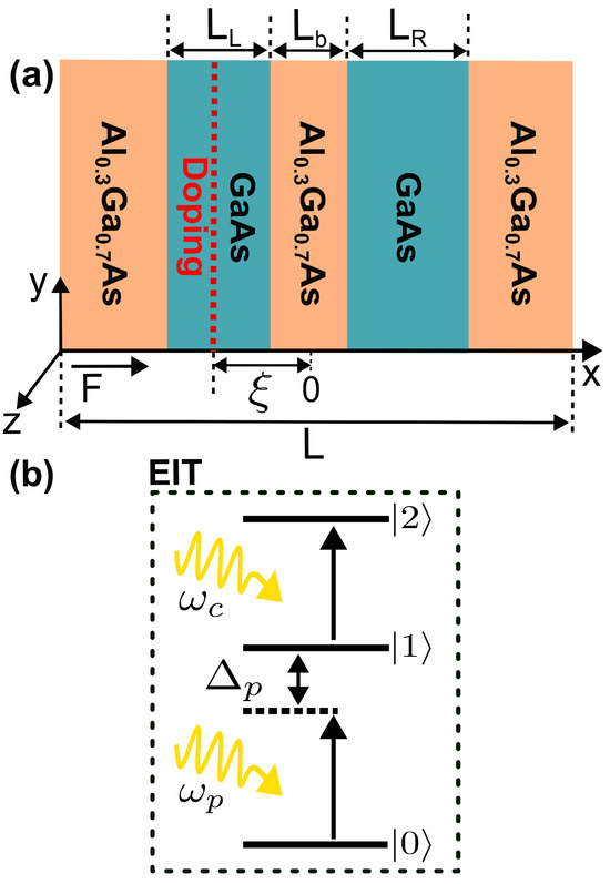
Figure 1.
(a) Schematic diagram of a GaAs/Al0.3Ga0.7
As double quantum well system centered at the origin of the x-axis subject to an external electric field F polarized along the heterostructure growth direction, with () denoting the left (right) well and the barrier width, respectively. The doping layer (dashed red line) of -width is inside the well (GaAs) at a separation from the origin. (b) Three-level ladder system configuration to study the electromagnetically induced transparency process.
2.2. The Self-Consistent Method
We first focus on determining the perturbation produced in the system by the electrostatic potential generated by the charge carriers and the ionized donor density within Hartree’s and effective-mass approximation. For this purpose, we begin with the time-independent Schrödinger equation
where ℏ is the reduced Planck constant, stands for the electron effective mass, assumed to be the same in both the well and the barrier regions, as well as the dielectric constant. Note that due to the low (30%) Al concentration in the GaAs/Al0.3Ga0.7As heterostructure, the discrepancy in the effective mass and dielectric constants does not significantly alter the energies of the system. The assumption is reasonably valid because the small difference between masses introduces only minor quantitative deviations in energy levels or wavefunction while simplifying calculations, as shown in Appendix A. is the j-th eigenfunction state with associated eigenvalue , and k indicates the k-th step in the self-consistent method. When , the self-consistent method only considers the electron confinement potential to solve the time-independent Schrödinger equation. For , we have the self-consistent potential , with 5% contribution of the Hartree perturbation potential , which allows us to achieve good numerical convergence in the electronic confinement potential. Following a similar procedure to that shown in Ref. [53], we solve Equation (2) via the finite difference method (FDM), obtaining a set of eigenfunctions and their associated eigenvalues .
Now, the charge neutrality condition (total number of electrons equal to the number of ionized donors per unit area) can be rewritten as [61]
where denotes a constant that involves the Boltzmann constant and the temperature of the system T, stands for the doped layer width, represents the Fermi energy, and are the k-th subband eigenvalue solutions from Equation (2). The presence of a delta-doped layer introduces a volumetric donor density (electrons per cubic meter), which will be equal to where the doped layer is located and is zero elsewhere. Note that in Equation (3) and the parameter table (Table 1), the term appears, which is a volumetric density of donors. However, the effective density that enters the procedure is a two-dimensional donor density (as can be evidenced in the left term of Equation (3) ()). Although it has been possible to start from a density per unit area, the three-dimensional expression has been chosen since, at an experimental level, volumetric densities are normally used. The above expressions allow us to obtain the corresponding eigenvalues and Fermi energy. Therefore, we can write the charge density related to the occupancy of the k-th iteraction as follows:

Table 1.
List of physical parameter values as implemented in the calculations [53].
The final step in our self-consistent approach is to calculate the electrostatic potential. For this purpose, we solve the equation defined by Poisson assuming a relatively high ionization in donor atoms for this material at room temperature ( K), so we have
where e represents the free electron charge and is the absolute permittivity. We use as a convergence criteria the Fermi energy , which establishes that the difference in the Fermi energy calculated in the k-th and ()-th step of the self-consistent method must be smaller than a given tolerance, thus,
In this way, we can obtain from the above expressions, the set of self-consistent solutions , and corresponding to the last step of the self-consistent method.
2.3. Electromagnetically Induced Transparency
We consider a three-level system in a ladder configuration, as shown in Figure 1b. The probe field incides upon the system with frequency , and the control field with frequency , coupling the states |0⟩ with |1⟩ and |1⟩ with |2⟩, respectively. Also, we include the effect of spontaneous emission between states through the decoherence rates ().
Implementing both the dipole and the rotating wave approximations, the Hamiltonian can be written as [37]:
where is the frequency of the n-th state (), is the probe field amplitude, is the electric dipole matrix element, and is the Rabi frequency associated with the transition .
We study the system dynamics through the Liouville–von Neumman equation, taking into account that the effects of decoherence are phenomenologically included [62], which leads to:
note that stands for the commutator and for the anticommutator, and corresponds to the dissipative rates due to spontaneous decay between states. Replacing Equation (7) into Equation (8), we can obtain a general compact expression for the matrix elements as follows:
where and are density matrix indexes, and is the Kronecker delta (0 if and 1 if ). are dissipative elements with non-diagonal terms. From Equation (9), we obtain the set of nine equations in the basis defined by the states |0⟩, |1⟩, and |2⟩. The density matrix is diagonal at thermal equilibrium. Its diagonal elements represent the populations of the energy levels , , establishing their relation to the Fermi energy via the Fermi–Dirac distribution. In particular, we are interested in obtaining the system’s absorption proportional to the density matrix . We assume that the entire electron population at is in the ground state, which means that , , and for , which is reasonable in the weak probe approximation.
To find the solution of the set of equations, we write Equation (9) in matrix form , where is a column vector and A is the square matrix associated with the coefficients of the system of equations. In this way, we obtain the solution through the expression [63]:
where is the eigenvectors matrix and the eigenvalues. Replacing and in Equation (9) and using Equation (10), we obtain the steady-state solution:
where is the detuning between the probe field frequency and the frequency of the transition.
The polarization of the probe field relates to the linear susceptibility coefficient of the system through . From this expression, and replacing the density matrix element , we obtain the imaginary () part of the linear susceptibility as follows [64]:
We assume that the value of the Rabi frequency has been fixed for the material. The LOAC is proportional to the imaginary part of the susceptibility, which allows us to calculate the EIT according to:
where c represents the speed of light in the medium .
Similarly, the LOAC has been calculated for the transition in the limit in Equation (13) (eliminating all contributions associated with the third level). In the EIT phenomenon, the probe laser continuously excites electrons from the ground state to the first excited state, while the control laser (with Rabi frequency ) simultaneously drives these electrons to the second excited state. When approaches zero, the control laser is effectively turned off, preventing electrons from reaching the second excited level. Consequently, assigning decay rates to that level becomes meaningless, and is automatically set to zero. As a result, the system no longer behaves as a three-level system, and the minimum in the EIT curve becomes a maximum in linear absorption, as reported in the literature [37,65].
3. Results and Discussion
This section examines the outcomes of the present study of the variation in the properties of the system schematized in Figure 1 with modifications in various geometric and non-geometric parameters.
Figure 2 shows the energy variation associated with the three lowest states and the Fermi level. In Figure 2a,c, the self-consistent potentials and the probability densities correspond to two fixed values of the right-hand well width. Specifically, Figure 2b depicts the energy variation with the width of the well on the right side from 2 nm to 20 nm for the three lowest states, maintaining the remaining parameters fixed at 8 nm, 5 nm, 2 nm, 0 kV/cm, and −6.5 nm (which corresponds to the center of the well on the left). We set the donor density cm−3 motivated by recent studies exploring densities of the order of cm−3 even cm−3 and reporting significant improvement in the optical and electronic properties as a consequence of modulated doping [66,67,68].
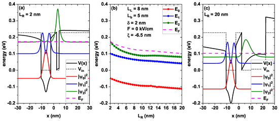
Figure 2.
(a,c) Self-consistent potential (solid black line) and electron confining potential (dashed black line) for GaAs/Al0.3Ga0.7
As, demonstrating two scenarios for the variations in the self-consistent potential seen by the electrons and probability densities (), with right-hand well width nm (a) and nm (c). In (b), the energy levels of the first three subbands as a function of the right-hand well width . Note that the energies associated with the states presented in (a,c) correspond to the minimum and maximum values of the parameter sweep, respectively.
As a consequence of the increase in , the states present a redshift caused by the decrease in confinement (taking the zero energy at the bottom of the well in the initial step, represented by the dashed black lines in Figure 2a,c); note how the electrons associated with the ground state remain in the delta layer region for the entire scan electrostatically attracted by the donor ions of that region.
From the entire sweep, it is straightforward that there is no change in symmetry in the presented wave functions and that all states remain occupied or semi-occupied (at least the second excited state) since they remain below the Fermi level represented by the dashed pink line. Considering the system is analyzed at room temperature, states close to the Fermi level cannot reach 100% occupancy. The immediate consequence of the latter is the possibility of performing an analysis of the optical properties for transitions to these levels.
Note that in both Figure 2a,c, the Fermi level lies above the first two confined levels—a consequence of the charges associated with ionized donors. One might infer that this implies no transitions between these states, as they are fully occupied. However, such a scenario would only occur at zero kelvin, where the electronic distribution function assumes a step-like form.
The results presented are for room temperature, which implies that the electronic distribution function does not have a step shape and, therefore, there is a non-zero probability of having completely unoccupied states below the Fermi level (strictly it would be the chemical potential) and occupied states above the said level (semi-occupied states). The above perfectly allows transitions to occur between states below the said level. As an additional test to ensure these transitions, the population difference associated with the transition between the ground state and the first excited level () has been calculated for Figure 2a,c, obtaining values of 1/cm3 and 1/cm3, respectively. These transitions below the Fermi level are perfectly validated and have been reported by various authors [69,70]. If the system were at low temperatures, these values would approach zero, preventing the probability of transition.
Figure 2a represents the system for the minimum sweep width, i.e., nm. The modification of the self-consistent potential due to the delta layer is observed, given that a deeper well is observed on the left side, coinciding with the delta layer position and generated by the total ionization of its donor atoms, which turns into a region of net positive charge. This figure also includes the probability densities of the three first low-lying confined states. The ground state is shown in red with an energy of −0.05 eV, and in blue and green, the first and second excited states, with energies of 0.1 eV and 0.17 eV, respectively. The self-consistent Fermi level has also been added as the dashed horizontal line that, in this configuration, takes a value of 0.173 eV.
Figure 2c represents the system for the maximum width of the well on the right ( 20 nm); again, the solid black curve represents the self-consistent potential modified by the donor density located at the center of the well on the left. Comparing with Figure 2a, we see that the minimum of the left barrier and on the left well moves towards lower energies; the same happens with the three lowest states whose energies are now −0.11 eV for the ground state, and 0.04 eV and 0.08 eV for the first and second excited states, respectively. Similarly, the Fermi level now takes the value of 0.102 eV. Note how the bottom of the band on the right-hand barrier takes, on the contrary, a higher energy value. It is worth highlighting the formation of a triangular quantum well in the well on the right where a non-negligible amount of electrons is located. This well is generated as a more notable effect between the redistribution of free electrons and the accumulation of ionized atoms in the well on the left.
Figure 3 shows the energy variation associated with the three first low-lying states and the Fermi level as a function of the external electric field intensity, F. In Figure 3a,c, the self-consistent potentials and probability densities corresponding to electric fields of and kV/cm are represented, respectively. As already mentioned, Figure 3b shows the variation in the energy of the three lowest states as a function of F from 0 to 33 kV/cm, maintaining fixed 8 nm, 9 nm, 5 nm, 2 nm, and −6.5 nm (which corresponds to the center of the well on the left).
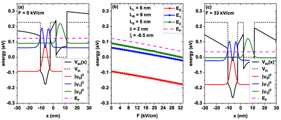
Figure 3.
(a,c) Modifications in the self-consistent potential of GaAs/Al0.3Ga0.7
As induced by the external electric field with kV/cm (a) and kV/cm (c). In (b), the energy levels of the first three subbands are shown as a function of the external electric field.
It is clear from Figure 3b, that as the external electric field F increases, the states present a monotonous redshift caused by the displacement of the bottom of the conduction band towards lower energies, which is a typical behavior of one-dimensional systems subjected to external electric fields. The largest number of electrons are located in the region of the delta layer attracted by the positive ions present in that region. Increasing the electric field intensity does not remarkably change the confining features of the central region, only introducing the above-discussed rigid shift in the conduction band minimum. The Fermi level exhibits behavior similar to the states: it is modulated by the external field, but no change in electronic occupation occurs. Notably, within the studied sweep range (as in Figure 2), there is no symmetry breaking in the wavefunctions.
Figure 3a shows the system for the minimum electric field of the sweep (0 kV/cm). In this figure, the self-consistent potential is modified only by the presence of the delta layer, which generates a deeper well in the area where it is located. The probability density for the three first low-lying states is also depicted with corresponding energies of −0.09 eV, 0.06 eV, and 0.09 eV, respectively, and the Fermi level with a value of 0.12 eV. As expected, the largest number of electrons in the ground state are concentrated in the doped layer”. In the second excited state (green curve), the electrons are mostly located in the well on the right, which constitutes the first state of this well and has a similar symmetry to that of the ground state. This shape is because the central barrier that separates the two wells does not allow a total interaction between them and, therefore, for this configuration, they are almost decoupled.
Figure 3c shows the system for the maximum sweep electric field (33 kV/cm). In contrast to what is shown in Figure 3a, the self-consistent potential is now found to be modified not only by the presence of the delta layer but also by the external electric field that induces a displacement of the electrons. As we will discuss later on, the electrostatic attraction between the ions and the charge carriers dominates over the external electric field effects, which is almost wholly screened in this region. As a consequence of the latter, the shape of the probability densities for the three states under study is noticeably similar to those obtained in Figure 3a; only a redshift is induced in the corresponding energies that take the values of −0.18 eV for the ground state, and −0.02 eV and −0.003 eV for the first and second excited states, respectively.
Figure 4 presents the three first low-lying energies and the Fermi level as a function of the position of the doped delta layer . In Figure 4a,c, the self-consistent potentials and probability densities that correspond to two fixed positions of the doped layer are represented. In Figure 4a, the layer has been fixed 2 nm to the left of the first well (−13 nm), while in Figure 4c, the layer has been set 2 nm on the right of the second well ( 15 nm)—these two positions are not equivalent since the width of the two wells differs by 1 nm. As already mentioned, Figure 4b shows the variation in the energy of the three first low-lying states as a function of from −13 to 15 nm, keeping the remaining parameters fixed as 8 nm, 9 nm, 5 nm, 2 nm, and 0 kV/cm; each of these figures is discussed in detail below.
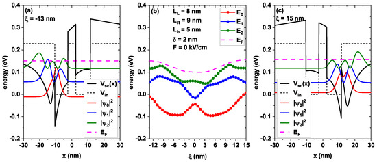
Figure 4.
(a,c) Modifications in the GaAs/Al0.3Ga0.7
As self-consistent potential induced by the location of the doped layer of -width with nm (a) and nm (c). In (b), the energy levels of the first three subbands are shown as a function of the doped delta layer location.
It is noticeable from Figure 4b that the position of the delta layer moves from left to right (varying ). The states present modifications of a different nature: the ground state moves to lower energies, reaching a local minimum at approximately −4.9 nm, corresponding to an approximate energy of −0.09 eV, which is the point where the maximum overlap between the well formed by the band offset of the heterostructure and the well formed by the donor ions of the doped delta layer occurs, causing the maximum deepening of the conduction band minimum at this point and, therefore, a shift to lower energy for the ground state. Something similar to the latter occurs when the delta layer is placed at approximately 4.7 nm, corresponding to an energy of about −0.1 eV, close to the center of the well on the right.
Note how for 0, a local maximum of the ground state energy occurs due to the creation of a third central well when locating the doped layer within the barrier zone, between the two original wells. This causes an increase in the energy associated with the conduction band minimum, which turns into a shift of the ground state towards higher energies (remembering that the zero energy remains fixed at the bottom of the wells for the self-consistent zero step, represented by the dashed black line).
Looking at Figure 4b, two anticrossings are found between the first and second excited states (blue and green curves, respectively) at −4.2 nm and 3.9 nm, as a consequence of the exchange of symmetry of the wave functions between these two states that takes place at those specific locations. The variation in the Fermi level is presented in this panel as well, a decrease in it being appreciable for −6 nm 6 nm, which could be because the delta-doped layer falls within the region of the central barrier, modifying the electronic confinement in such a way that the first two energy levels tend to couple and interact with each other, generating an anticrossing (which decreases the first excited state energy) and, additionally, the carrier density in the system does not change. The second excited level decreases in energy; consequently, the Fermi level also decreases.
Figure 4a,c show the system for the minimum and maximum positions of the delta layer −13 nm and 15 nm, respectively. Both figures show the self-consistent potential modified only by the presence of the doped layer at 2 nm from each well, which generates an additional well of smaller depth near the nearest well. Note how introducing this delta layer modifies the shape of both wells, deepening the one closest to it. In addition, the system’s symmetry comes to light making the depth modification greater in the narrower well. The fact of having a deeper well generates a higher electron accumulation in the area, which is evident by comparing the probability density of the state fundamental (red curve) in Figure 4a,c. The energy levels in these two figures are very similar, with a small difference caused by the intentional asymmetry added with the increase in 1 nm of the width of the well on the right . In the particular case of Figure 4a, these values are as follows: −0.01 eV for the ground state and 0.06 eV and 0.12 eV for the first and second excited states, respectively.
Figure 5 presents the three first low-lying energies together with the Fermi level in the double well system subjected to variations in the width of the doped delta layer, maintaining its position in the center of the well on the left. In Figure 5a,c, the self-consistent potentials and probability densities corresponding to two fixed widths of the delta layer are represented. In Figure 5a, the width of the layer has been set to 1 nm, while in Figure 5c, it has been set to 4 nm, keeping the position fixed. Figure 5b shows the dependence of the three first states energy on , ranging from 1 to 4 nm, keeping the remaining parameters fixed as 8 nm, 9 nm, 5 nm, −6.5 nm, and 0 kV/cm.
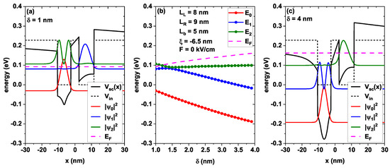
Figure 5.
(a,c) Modifications in the GaAs/Al0.3Ga0.7
As self-consistent potential induced by the doped layer width with nm (a) and nm (c). In (b), the energy levels of the first three subbands are shown as a function of the doped delta layer width.
As already mentioned, Figure 5b presents the variation in the energy with increasing delta layer widths. It is clear that the states undergo significant modifications throughout the range of the sweep; the ground state evolves monotonically towards lower energies, decreasing from −0.03 eV for 1 nm to −0.19 eV for 4 nm. This decrease is caused by the increase in the well depth originating from the increment in the width of the delta layer that shifts the bottom of the conduction band towards lower energies. This is clearly explained since by increasing the doped region while keeping the volumetric density of donors fixed, the number of ionized atoms must increase and, therefore, the electrostatic attraction of positive charges is greater, which generates a deeper well for greater , as is evidenced by comparing the self-consistent potential in Figure 5a with Figure 5c.
In Figure 5b, an anticrossing is found between the first and second excited states for 1.5 nm, representing the interaction and coupling between these states. As a consequence of this anticrossing, a symmetry change is generated between the two states involved, as can be seen by comparing the blue and green curves in Figure 5a,c. Note how the Fermi level (represented by the dashed pink line) presents a blueshift as the width of the doped delta layer increases. This is because the volumetric donor density is fixed and the volume of the doped region increases, which translates to a higher number of charge carriers. Meanwhile, as the Fermi level is proportional to the number of charge carriers, the ascending behavior shown in the figure corresponds to what is expected. In this same sense, it should be noted that for 1 nm, the second excited state is above the Fermi level, while for 4 nm, it is now considerably below the Fermi level, according to the increase in the number of electrons.
As a consequence of the characteristics of the doped delta layer, such as position or width, an electric field is generated in the barrier region, as evidenced in Figure 2, Figure 3, Figure 4 and Figure 5. Table 2 presents an estimate of the value of the aforementioned electric field, where a negative field emerges in Figure 4c caused by the position of the doped delta layer to the right of the wider well. On the other hand, the greater magnitude of the electric field in Figure 5c is caused by the strong electrostatic attraction of ionized atoms concentrated in a delta layer of wider width.
Table 2.
The estimated electric field along the x-axis for the central barrier is shown in each figure.
Figure 6 shows the self-consistent electron density obtained according to Equation (4) normalized in the donor density in terms of the coordinate x for the minimum and maximum widths of the well on the right (Figure 6a), with zero electric field and with the maximum electric field considered (Figure 6b), locating the delta layer at two different x-values (Figure 6c), and for the two considered widths of the delta layer (Figure 6d).
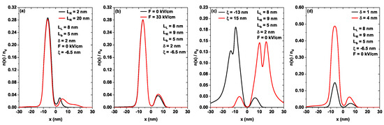
Figure 6.
(a–d) Electron density in terms of the x-coordinate for different configurations of the double quantum well. Two different values are shown for the width of the right-hand well (a), the applied electric field (b), the doped layer position (c), and the width of the doped layer (d).
Figure 6a shows the variation in for 2 nm (black curve) and 20 nm (red curve), keeping the remaining parameters fixed as 8 nm, 5 nm, −6.5 nm, 2 nm, and 0 kV/cm. As previously shown in Figure 2a,b, the increase in the width of the well on the right generates a small but significant electron accumulation in it, but keeping the distribution practically unaltered, given that the ground and the first excited states remain in the left well centered on the position of the doped delta layer. From the above, and comparing the black and red curves, it is evident that the position of the maximum in the graph is located at . The change in the magnitude of the peak on the left in the density is minimal. The significant modification is presented for the region on the right of the density that is modified by accumulating more electrons and distributing them over a larger area (compare black and red curve for ).
Figure 6b shows the variation in without including the electric field 0 kV/cm (black curve) and with the electric field 33 kV/cm (red curve), keeping the remaining parameters fixed as 8 nm, 9 nm, 5 nm, −6.5 nm, and 2 nm. For this heterostructure, an increase in the intensity of the electric field does not generate significant changes in the electron’s position; for 33 kV/cm, only a small fraction of the electrons move from the well on the left towards the well on the right (compare black and red curve for ), remaining attracted mainly by the dominant effect of the positive ions located at . The above could be explained, as already mentioned in Figure 3, because the electric field does not modify the ground state position and the first excited state, maintaining them always inside the well on the left; only the second excited state can be modified, but this is a low probability state.
Figure 6c shows the variation in for two different delta layer positions: for −13 nm (black curve), the delta layer is located 2 nm to the left of the well width , and for 15 nm (red curve), the delta layer is located 2 nm to the right of the well width ; all remaining parameters have been set to 8 nm, 9 nm, 5 nm, 2 nm, and 0 kV/cm. When the delta layer is located at −13 nm, two local maxima are generated in the electron density curve, one for −13.3 nm, with a magnitude of approximately 0.13 (dimensionless since it is the ratio ) and another at −9.4 nm, with an approximate magnitude of 0.18. This indicates that the largest number of electrons are located inside of the well of width , not in the well created by the delta layer, which is of smaller width. When the delta layer is located at 15 nm (red curve), the difference in confinement between the well of width and the well produced by the doped delta layer becomes smaller, which implies that the electrons are distributed similarly in both regions (note the division of the ground state probability density in the red curve of Figure 4c). This behavior is evident from the two local maxima that the figure presents for 10.2 nm and 15.6 nm, with approximate magnitudes of 0.14. Note how the electron density does not tend to zero for 30 nm, due to the contribution and occupation of the higher states that are more extended.
Finally, Figure 6d presents the variation in for two different delta layer widths, for 1 nm (black curve) and for 4 nm (red curve); all remaining parameters have been set to 8 nm, 9 nm, 5 nm, −6.5 nm, and 0 kV/cm. Both for 1 nm and 4 nm, the electrons are mostly located in the delta shell region, although there is a small probability of finding electrons within the well on the right. Note how the electron density associated with 4 nm is greater in magnitude, because by increasing the width of the doped region (), its volume region also increases. As the volumetric density of donors has been maintained fixed, the number of charge carriers must be increased, accumulating in that region.
Figure 7 presents the product with respect to in Figure 7a, as a function of F in Figure 7b, as a function of in Figure 7c, and in terms of in Figure 7d, where is the square modulus of the dipole matrix element corresponding to the transition from the ground state to the first excited state and is the corresponding transition energy. The product is important since according to Equations (12) and (13), it is evident that the absorption associated with the EIT is proportional to this product. In the panel of Figure 7, three points have been highlighted, corresponding to notable values, such as local maximums or minimums, for example (see dashed red, blue, and green vertical lines). These points are considered later for the EIT analysis.
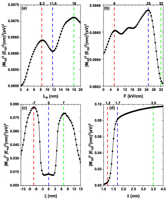
Figure 7.
The product with respect to the right-hand well width (a), of the externally applied electric field intensity (b), of the doped layer position (c), and of the doped layer width (d). For each figure, the parameters are the same as those in Figure 1, Figure 2, Figure 3, Figure 4 and Figure 5.
Analyzing the vertical axes of each figure, it is evident that the change in in the range presented is approximately nm2 eV2 for Figure 7a, nm2 eV2 for Figure 7b, from nm2 eV2 for Figure 7c, and nm2 eV2 for Figure 7d. The above indicates that there is a difference of approximately three orders of magnitude in the range of variation of the product between Figure 7a,d. This difference is significant and has important implications for the magnitude of the EIT peaks, as will be seen later.
Figure 8 shows the EIT variation with the incident photon energy () in a contour graph according to the color scale presented on the right, where changes in the EIT are simultaneously analyzed for the variation in (Figure 8a), varying F (Figure 8b), varying (Figure 8c), and varying (Figure 8d). In each figure, the parameters that do not vary are kept fixed as previously mentioned in Figure 2, Figure 3, Figure 4 and Figure 5. Additionally, in each panel, a set of points has been added, corresponding to the energy of the transition from the ground to the first excited states (pink dots) in order to clarify that the maximum absorption peak is located between the two peaks generated by EIT, coinciding with its minimum. In each panel, three different values of the studied parameter have also been chosen (red, blue, and green horizontal lines) in order to graph the associated EIT and compare their magnitude and relative peak positions (red, blue, and green curves at the top of each outline image). The three selected values perfectly match the positions of the dashed vertical lines depicted in Figure 7.
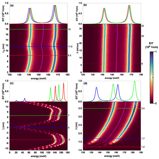
Figure 8.
(a–d) 2D contour plots for the electromagnetically induced transparency as a function of the photon energy. In (a), the effect of variations in the width of the right-hand well, the applied electric field (b), the location of the doped layer (c), and the width of the doped layer (d). For each figure, the parameters are the same as those in Figure 1, Figure 2, Figure 3, Figure 4 and Figure 5.
Figure 8a illustrates the variation in EIT for a complete sweep of . In the entire range presented, there are no significant changes in the magnitude of the EIT peaks with increasing since, according to Figure 7a, the maximum difference that would be expected should be of the order of . On the other hand, the transition energy does not change beyond 10 meV; for this reason, no significant changes are found for the three EIT curves shown at the top of this figure.
Figure 8b shows the variation in EIT for a sweep of the external electric field F. As in Figure 8a, in the presented range of the field, no significant changes are evident in the magnitude of the EIT peaks. This is because the maximum change of the peaks should be of the order of , according to the results of Figure 7b. Likewise, there is practically no change in the transition energy , which implies that both the location and magnitude of the EIT peaks remain practically unaffected by changes in the external electric field in the range under study. Figure 8c shows the variation in EIT varying the doped delta layer position, . In this figure, in contrast with Figure 8a,b, a significant alteration in both the magnitude and position of the EIT peaks is appreciated. For the three particular values of considered, peaks of greater magnitude are presented for −7 nm, followed by 7 nm, and the peaks of lowest magnitude are found for . This behavior is explained through the previous results obtained in Figure 7c, where a similar behavior is observed for the product for the same values of . Likewise, the possibility of shifting the EIT peaks is clear since the transition energy for this case largely changes with the position of the doped delta layer.
Figure 8d shows the variation in EIT with increase in the width of the doped delta layer , keeping its position fixed in the left well, as in Figure 8c. This figure also shows significant changes in the magnitude, position, and separation between the EIT peaks. The low magnitude of the peaks for 1.2 nm compared to the peaks generated for 3.5 nm is remarkable; this difference corresponds to what is shown in Figure 7d. As in the case of the change in magnitude, the change in the peak location follows the behavior of the transition energy between the ground state and the first excited state.
The results presented in this figure show the possibility of tuning the separation, magnitude, and position of the EIT peaks by modulating the position and width of the doping layers, either in the barrier region or in the QWs, enabling the system to solve close frequencies or to distinguish between very close transitions, which is useful in applications such as quantum spectroscopy.
The shaded curves in Figure 9a,b illustrate the LOAC for the transition between the |0⟩ and |1⟩ states, while the unshaded curves show the EIT [Equation (12)] as a function of the photon energy. In each case, one parameter is varied, keeping the other fixed at their respective values, as follows: nm, nm, nm, and 1/cm3, nm and nm. Figure 9a shows the effect of varying the doped layer position along the heterostructure. When the doped layer is located at the center of the heterostructure ( nm), both LOAC and EIT present a significantly lower intensity compared to nm, where a maximum is reached. This can be justified by the existing relation between the dipole moment matrix element , which measures the superposition of the wave functions of the |0⟩ and |1⟩ states, and the transition energy . When the doped layer is at nm, coinciding with a potential barrier, an additional confining region is generated. This confinement alters the distribution of the wave functions, and the transition energy decreases, which translates to lower LOAC and EIT intensities. In contrast, at nm, there is a displacement of the doped layer that induces a blueshift in the resonances, causing an increase in the energy separation of the confined levels. The effect of varying the width of the doped layer for nm and nm is shown in Figure 9b. It is straightforward that an increment in the doped layer width results in an increase in the amplitude of the peaks in the LOAC and EIT, in addition to a blueshift. This behavior is a consequence of the increase in the number of positive ions, generated by the broadening of the doped layer, which modifies the effective potential within the doped region, which is reflected in the depth of the confining regions in the heterostructure. This structural change introduces new energy levels and the carrier distribution changes significantly, affecting both the optical transition probability and the transition energy.
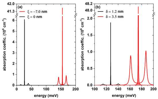
Figure 9.
Linear optical absorption coefficient (shaded curves), and electromagnetically induced transparency (unshaded curves) with respect to the incident photon energy. In (a) the effect of the position of the doped layer with -width, in (b) the effect of the doped layer position. For each panel, the parameters are the same as those in Figure 1, Figure 2, Figure 3, Figure 4 and Figure 5.
4. Conclusions
In this work, a theoretical study of the EIT in an asymmetric GaAs/AlGaAs double quantum well system was performed, considering the effects of a modulated n-doped layer, structural variations, and the presence of external electric fields. Using the FDM, we self-consistently solved the Schrödinger equation, the Poisson equation, and the charge neutrality condition, which allowed us to analyze how the effective potential, determined by the carrier density, influences the optical properties of the system.
The analyzed parameters in this study significantly influence the EIT since it depends on quantum confinement and dipolar interaction between the electronic states. In the presence of an external electric field, the states show a redshift caused by the displacement at low energies of the bottom of the conduction band. This causes many electrons to be attracted to the positive ions in the doped-layer region. Increasing the width of the right-hand well causes a decrease in confinement. It shifts the lower energies to the bottom of the conduction band, resulting in a redshift of the optical resonances. On the other hand, the position of the doped layer affects the wave functions overlap for the confined states, which modulates the dipole array element, which is of key relevance in EIT efficiency. When the doped layer is close to the central barrier, the lower energy levels interact and generate anticrossings, which modify both the intensity and spectral position of the optical transitions. In addition, an increase in the doped region width deepens the effective well, increasing the electron density in specific areas and strengthening the associated optical transitions, albeit at the expense of a spectral shift.
Our results demonstrate that an external electric field, structural parameters, and delta doping fit the necessary conditions for the occurrence of an EIT-like effect, allowing for a more accurate design of optoelectronic devices, such as photodetectors, optical switches, laser diodes, and infrared detectors. These results are significant because they demonstrate an effective tuning of the frequencies that induce EIT as an optical response in the double quantum well system, a phenomenon not previously reported. Such modulation can be achieved through modifications in doping characteristics and the application of external electric fields, as evidenced by the results. The present analysis of EIT in double-well heterostructures can be extended to studies involving different materials and a variety of geometries. The analysis of the and V configurations for EIT in this system is currently underway and will be published elsewhere.
Author Contributions
C.A.D.-C. and J.A.G.-C.: Conceptualization, methodology, software, formal analysis, investigation, writing; R.V.H.H.: Formal analysis, investigation, writing; A.L.M.: Formal analysis, investigation, supervision; R.L.R., M.E.M.-R. and C.A.D.: Formal analysis, writing. All authors have read and agreed to the published version of the manuscript.
Funding
The authors would like to thank the Colombian Agencies: CODI-Universidad de Antioquia (Estrategia de Sostenibilidad de la Universidad de Antioquia and projects “Complejos excitónicos y propiedades de transporte en sistemas nanométricos de semiconductores con simetría axial basados en GaAs e InAs”, and “Nanoestructuras semiconductoras con simetría axial basadas en InAs y GaAs para aplicaciones en electrónica ultra e híper rápida”) and Facultad de Ciencias Exactas y Naturales-Universidad de Antioquia (C.A.D. and A.L.M. exclusive dedication project 2025–2026). R.V.H.H. gratefully acknowledges financial support from the Spanish Junta de Andalucía through a Doctoral Training Grant PREDOC-01408. R.L.R would like to thank the Universidad EIA, Colombia, through the project “Simulación por el método de elementos finitos de las respuestas ópticas de nanoestructuras semiconductoras aplicadas en imágenes médicas” (Código: INVIM0442023).
Institutional Review Board Statement
Not applicable.
Informed Consent Statement
Not applicable.
Data Availability Statement
The original contributions presented in the study are included in the article, further inquiries can be directed to the corresponding authors.
Conflicts of Interest
The authors declare no conflicts of interest.
Appendix A
Figure A1a,c show the probability densities considering the same mass both in well and barrier regions (solid lines, as shown in Figure 2) and distinguishing between the corresponding values associated to well () and barrier () (dots). The two curves nearly overlap, with the only difference occurring at the maximum energy values. In contrast, Figure A1b shows a complete overlap in the energy curves as a function of the right-hand well width. These results suggest that mass differences between the well and barrier regions induce only minor changes in the probability densities and energies.
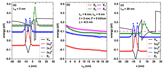
Figure A1.
(a,c) Self-consistent potential (solid black line) and electron confining potential (dashed black line) for GaAs/Al0.3Ga0.7
As, demonstrating two scenarios for the variations in the self-consistent potential seen by the electrons and probability densities (), with right-hand well width nm (a) and nm (c). In (b), the energy levels of the first three subbands as a function of the right-hand well width . Coloured solid lines show the results obtained assuming the same effective mass for well and barrier, whereas dots represent the results obtained distinguishing the effective masses of well () and barrier ().
References
- Wood, C.E.C.; Metze, G.; Berry, J.; Eastman, L.F. Complex free-carrier profile synthesis by “atomic-plane” doping of MBE GaAs. J. Appl. Phys. 1980, 51, 383. [Google Scholar] [CrossRef]
- Liu, D.G.; Lee, C.P.; Chang, K.H.; Wu, J.S.; Liou, D.C. Delta-doped quantum well structures grown by molecular beam epitaxy. Appl. Phys. Lett. 1990, 57, 1887–1888. [Google Scholar] [CrossRef]
- Hoenk, M.E.; Grunthaner, P.J.; Grunthaner, F.J.; Terhune, R.W.; Fattahi, M.; Tseng, H.F. Growth of a delta-doped silicon layer by molecular beam epitaxy on a charge-coupled device for reflection-limited ultraviolet quantum efficiency. Appl. Phys. Lett. 1992, 61, 1084–1086. [Google Scholar] [CrossRef]
- Su, Y.K.; Wang, R.L.; Tsai, H.H. Delta-doping interband tunneling diode by metal-organic chemical vapor deposition. IEEE Trans. Electron. Devices 1993, 40, 2192–2198. [Google Scholar]
- Liliental-Weber, Z.; Benamara, M.; Swider, W.; Washburn, J.; Grzegory, I.; Porowski, S.; Lambert, D.J.H.; Eiting, C.J.; Dupuis, R.D. Mg-doped GaN: Similar defects in bulk crystals and layers grown on Al2O3 by metal-organic chemical-vapor deposition. Appl. Phys. Lett. 1999, 75, 4159–4161. [Google Scholar] [CrossRef]
- Wyrick, J.; Wang, X.; Kashid, R.V.; Namboodiri, P.; Schmucker, S.W.; Hagmann, J.A.; Liu, K.; Stewart, M.D., Jr.; Richter, C.A.; Bryant, G.W.; et al. Atom-by-atom fabrication of single and few dopant quantum devices. Adv. Funct. Mater. 2019, 29, 1903475. [Google Scholar] [CrossRef]
- McCandless, J.P.; Protasenko, V.; Morell, B.W.; Steinbrunner, E.; Neal, A.T.; Tanen, N.; Cho, Y.; Asel, T.J.; Mou, S.; Vogt, P.; et al. Controlled Si doping of β-Ga2O3 by molecular beam epitaxy. Appl. Phys. Lett. 2022, 121, 072108. [Google Scholar] [CrossRef]
- Hakl, M.; Lin, Q.; Lepillet, S.; Billet, M.; Lampin, J.-F.; Pirotta, S.; Colombelli, R.; Wan, W.; Cao, J.C.; Li, H.; et al. Ultrafast quantum-well photodetectors operating at 10 μm with a flat frequency response up to 70 GHz at room temperature. ACS Photonics 2021, 8, 464–471. [Google Scholar] [CrossRef]
- Jeannin, M.; Cosentino, E.; Pirotta, S.; Malerba, M.; Biasiol, G.; Manceau, J.M.; Colombelli, R. Low-intensity saturation of an ISB transition by a mid-IR quantum cascade laser. Appl. Phys. Lett. 2023, 122, 24. [Google Scholar] [CrossRef]
- Malerba, M.; Pirotta, S.; Aubin, G.; Lucia, L.; Jeannin, M.; Manceau, J.-M.; Bousseksou, A.; Lin, Q.; Lampin, J.-F.; Peytavit, E.; et al. Ultrafast (≈10 GHz) mid-IR modulator based on ultrafast electrical switching of the light-matter coupling. Appl. Phys. Lett. 2024, 125, 4. [Google Scholar] [CrossRef]
- Pirotta, S.; Tran, N.L.; Jollivet, A.; Biasiol, G.; Crozat, P.; Manceau, J.M.; Colombelli, R. Fast amplitude modulation up to 1.5 GHz of mid-IR free-space beams at room-temperature. Nat. Commun. 2021, 12, 799. [Google Scholar] [CrossRef] [PubMed]
- Schubert, E.F.; Fischer, A.; Ploog, K. The delta-doped field-effect transistor (δFET). IEEE Trans. Electron. Devices 1986, 33, 625–632. [Google Scholar] [CrossRef]
- Krishnamoorthy, S.; Xia, Z.; Bajaj, S.; Brenner, M.; Rajan, S. Delta-doped β-gallium oxide field-effect transistor. Phys. Express 2017, 10, 051102. [Google Scholar]
- Cingolani, R.; Lomascolo, M.; Lovergine, N.; Dabbicco, M.; Ferrara, M.; Suemune, I. Excitonic properties of ZnSe/ZnSeS superlattices. Appl. Phys. Lett. 1994, 64, 2439–2441. [Google Scholar] [CrossRef]
- Fickenscher, M.; Shi, T.; Jackson, H.E.; Smith, L.M.; Yarrison-Rice, J.M.; Zheng, C.; Miller, P.; Etheridge, J.; Wong, B.M.; Gao, Q.; et al. Optical, structural, and numerical investigations of GaAs/AlGaAs core–multishell nanowire quantum well tubes. Nanophotonics 2013, 13, 1016–1022. [Google Scholar] [CrossRef]
- Prete, P.; Wolf, D.; Marzo, F.; Lovergine, N. Nanoscale spectroscopic imaging of GaAs-AlGaAs quantum well tube nanowires: Correlating luminescence with nanowire size and inner multishell structure. Nanophotonics 2019, 8, 1567–1577. [Google Scholar] [CrossRef]
- Degani, M.H. Electron energy levels in a δ-doped layer in GaAs. Phys. Rev. B 1991, 44, 5580. [Google Scholar] [CrossRef]
- Calcagnile, L.; Rinaldi, R.; Prete, P.; Stevens, C.J.; Cingolani, R.; Vanzetti, L.; Sorba, L.; Franciosi, A. Free-carrier effects on the excitonic absorption of n-type modulation-doped Zn1-xCdxSe/ZnSe multiple quantum wells. Phys. Rev. B 1995, 52, 17248. [Google Scholar] [CrossRef]
- Tulupenko, V.; Duque, C.A.; Akimov, V.; Demediuk, R.; Belykh, V.; Tiutiunnyk, A.; Fomina, O. On intersubband absorption of radiation in delta-doped QWs. Phys. E Low Dimens. Syst. Nanostruct. 2015, 74, 400–406. [Google Scholar] [CrossRef]
- Wang, K.F.; Gu, Y.; Yang, X.; Yang, T.; Wang, Z. Si delta doping inside InAs/GaAs quantum dots with different doping densities. J. Vac. Sci. Technol. B 2012, 30, 041808. [Google Scholar] [CrossRef]
- Bendayan, M.; Belhassen, J.; Karsenty, A. Modulated Photoluminescence at Low Temperature Measurements with Controlled Electron Concentration in Asymmetric GaAs/GaAlAs/GaAs Quantum Wells. J. Lumin. 2022, 250, 119109. [Google Scholar] [CrossRef]
- Khakshoor, A.; Belhassen, J.; Bendayan, M.; Karsenty, A. Doping modulation of self-induced electric field (SIEF) in asymmetric GaAs/GaAlAs/GaAs quantum wells. Results Phys. 2022, 32, 105093. [Google Scholar] [CrossRef]
- Sánchez-Martínez, E.H.; López-López, M.; Méndez-Camacho, R.; Yee-Rendón, C.M.; Zambrano-Serrano, M.A.; López-Luna, E.; Cruz-Hernández, E. Nonlocal Si δ-doping in horizontally-aligned GaAs nanowires. Surf. Interfaces 2025, 56, 105580. [Google Scholar] [CrossRef]
- Swain, R.C.; Sahu, A.K.; Sahoo, N. Modulation of electron transport and quantum lifetimes in symmetric and asymmetric AlGaAs/InGaAs double quantum well structures. Jpn. J. Appl. Phys. 2023, 63, 014001. [Google Scholar] [CrossRef]
- Sužiedėlis, A.; Ašmontas, S.; Gradauskas, J.; Čerškus, A.; Šilėnas, A.; Lučun, A. Impact of buffer layer on electrical properties of bow-tie microwave diodes on the base of MBE-grown modulation-doped semiconductor structure. Crystals 2025, 15, 50. [Google Scholar] [CrossRef]
- Yang, X.; Wang, K.; Gu, Y.; Ni, H.; Wang, X.; Yang, T.; Wang, Z. Improved efficiency of InAs/GaAs quantum dots solar cells by Si-doping. Sol. Energy Mater. Sol. Cells 2013, 30, 144–147. [Google Scholar] [CrossRef]
- Firsov, D.A.; Vorobjev, L.E.; Vinnichenko, M.Y.; Balagula, R.M.; Kulagina, M.M.; Vasil’iev, A.P. Effect of transverse electric field and temperature on light absorption in GaAs/AlGaAs tunnel-coupled quantum wells. Semiconductors 2022, 49, 1425–1429. [Google Scholar] [CrossRef]
- Dakhlaoui, H.; Nefzi, M. Tuning the linear and nonlinear optical properties in double and triple δ-doped GaAs semiconductor: Impact of electric and magnetic fields. Superlattices Microstruct. 2019, 136, 106292. [Google Scholar] [CrossRef]
- Rodríguez-Magdaleno, K.A.; Martínez-Orozco, J.C.; Rodríguez-Vargas, I.; Mora-Ramos, M.E.; Duque, C.A. Asymmetric GaAs n-type double δ-doped quantum wells as a source of intersubband-related nonlinear optical response: Effects of an applied electric field. Superlattices Microstruct. 2014, 147, 77–84. [Google Scholar] [CrossRef]
- Salman Durmuslar, A.; Dakhlaoui, H.; Mora-Ramos, M.E.; Ungan, F. Effects of external fields on the nonlinear optical properties of an n-type quadruple δ-doped GaAs quantum wells. Eur. Phys. J. Plus 2022, 137, 730. [Google Scholar] [CrossRef]
- Dakhlaoui, H.; Belhadj, W.; Durmuslar, A.S.; Ungan, F.A.T.I.H.; Abdelkader, A. Numerical study of optical absorption coefficients in Manning-like AlGaAs/GaAs double quantum wells: Effects of doped impurities. Phys. E Low Dimens. Syst. Nanostruct. 2023, 147, 115623. [Google Scholar] [CrossRef]
- Noverola-Gamas, H.; Rojas, L.M.; Azalim, S.; Oubram, O. Disorder effect on intersubband optical absorption of n-type δ-doped quantum well in GaAs. J. Condens. Matter Phys. 2023, 35, 405602. [Google Scholar] [CrossRef] [PubMed]
- Jaouane, M.; Ed-Dahmouny, A.; Arraoui, R.; Althib, H.M.; Fakkahi, A.; El Ghazi, H.; Zeiri, N. Delta-doping modulation of three quantum wells under the influence of an electric field. APL Mater. 2024, 12, 101106. [Google Scholar] [CrossRef]
- Sari, H.; Ungan, F.; Sakiroglu, S.; Yesilgul, U.; Sökmen, I. The effects of intense laser field on optical responses of n-type delta-doped GaAs quantum well under applied electric and magnetic fields. Optik 2018, 162, 76–80. [Google Scholar] [CrossRef]
- Saidi, I. Evaluation of second harmonic generation susceptibility in a delta-doped AlGaAs/GaAs asymmetric Gaussian potential. Micro Nanostruct. 2022, 163, 107136. [Google Scholar] [CrossRef]
- Schmidt, H.; Imamoǧlu, A. High-speed properties of a phase-modulation scheme based on electromagnetically induced transparency. Opt. Lett. 1998, 23, 1007–1009. [Google Scholar] [CrossRef]
- Fleischhauer, M.; Imamoǧlu, A.; Marangos, J.P. Electromagnetically induced transparency: Optics in coherent media. RMP 2005, 77, 633–673. [Google Scholar] [CrossRef]
- Abdumalikov, A.A., Jr.; Astafiev, O.; Zagoskin, A.M.; Pashkin, Y.A.; Nakamura, Y.; Tsai, J.S. Electromagnetically induced transparency on a single artificial atom. Phys. Rev. Lett. 2010, 104, 193601. [Google Scholar] [CrossRef]
- Ek, S.; Lunnemann, P.; Chen, Y.; Semenova, E.; Yvind, K.; Mork, J. Slow-light-enhanced gain in active photonic crystal waveguides. Opt. Lett. 2014, 5, 5039. [Google Scholar] [CrossRef]
- Xue, W.; Yu, Y.; Ottaviano, L.; Chen, Y.; Semenova, E.; Yvind, K.; Mork, J. Threshold characteristics of slow-light photonic crystal lasers. Phys. Rev. Lett. 2016, 116, 063901. [Google Scholar] [CrossRef]
- Khurgin, J.B.; Tucker, R.S. Slow Light: Science and Applications; CRC Press: Boca Raton, FL, USA, 2018. [Google Scholar]
- Beausoleil, R.G.; Munro, W.J.; Rodrigues, D.A.; Spiller, T.P. Applications of electromagnetically induced transparency to quantum information processing. Micro Nanostruct. 2004, 51, 2441–2448. [Google Scholar] [CrossRef]
- Chang, D.E.; Vuletić, V.; Lukin, M.D. Quantum nonlinear optics—Photon by photon. Nat. Photon. 2014, 8, 685–694. [Google Scholar] [CrossRef]
- Meyer, D.H.; O’Brien, C.; Fahey, D.P.; Cox, K.C.; Kunz, P.D. Optimal atomic quantum sensing using electromagnetically-induced-transparency readout. Phys. Rev. A 2021, 104, 043103. [Google Scholar] [CrossRef]
- Zhong, J.; Xu, X.; Lin, Y.S. Tunable terahertz metamaterial with electromagnetically induced transparency characteristic for sensing application. Phys. Rev. A 2021, 11, 2175. [Google Scholar] [CrossRef]
- Hameed, A.H.; Al-Khursan, A.H. Engineering of plasmonic electromagnetically induced transparency from double quantum dot-metal nanoparticle structure. J. Nanophotonics 2024, 18, 026003. [Google Scholar] [CrossRef]
- Bejan, D. Electromagnetically induced transparency in double quantum dot under intense laser and magnetic fields: From Λ to Σ configuration. Eur. Phys. J. B 2017, 90, 54. [Google Scholar] [CrossRef]
- Bejan, D. Effects of electric field and structure on the electromagnetically induced transparency in double quantum dot. Opt. Mater. 2017, 67, 145. [Google Scholar] [CrossRef]
- Bejan, D.; Stan, C.; Niculescu, E.C. Effects of electric field and light polarization on the electromagnetically induced transparency in an impurity doped quantum ring. Opt. Mater. 2018, 75, 827. [Google Scholar] [CrossRef]
- Naghdi, E.; Sadeghi, E.; Zamani, P. Electromagnetically induced transparency in coupled quantum dot-ring structure under external electric field and donor impurity. Chin. J. Phys. 2018, 56, 2139. [Google Scholar] [CrossRef]
- Pavlović, V.; Susnjar, M.; Petrović, K.; Stevanović, L. Electromagnetically induced transparency in a multilayered spherical quantum dot with hydrogenic impurity. Opt. Mater. 2018, 78, 191. [Google Scholar] [CrossRef]
- Jayarubi, J.; John Peter, A.; Lee, C.W. Electromagnetically induced transparency in a GaAs/InAs/GaAs quantum well in the influence of laser field intensity. Eur. Phys. J. D 2019, 73, 63. [Google Scholar] [CrossRef]
- Gil-Corrales, J.A.; Morales, A.L.; Duque, C.A. Self-consistent study of GaAs/AlGaAs quantum wells with modulated doping. Nanomaterials 2023, 13, 913. [Google Scholar] [CrossRef] [PubMed]
- Sun, G.; Khurgin, J.B.; Friedman, L.; Soref, R.A. Tunable intersubband Raman laser in GaAs/AlGaAs multiple quantum wells. J. Opt. Soc. Am. B 1998, 15, 648. [Google Scholar] [CrossRef]
- Choi, J.K.; Vagidov, N.; Sergeev, A.; Kalchmair, S.; Strasser, G.; Vasko, F.; Mitin, V. Asymmetrically doped GaAs/AlGaAs double-quantum-well structure for voltage-tunable infrared detection. Jpn. J. Appl. Phys. 2012, 51, 7R. [Google Scholar] [CrossRef]
- Kumari, B.; Kattayat, S.; Kumar, S.; Kaya, S.; Katti, A.; Alvi, P.A. Improved and tunable optical absorption characteristics of MQW GaAs/AlGaAs nano-scale heterostructure. Optik 2020, 208, 164544. [Google Scholar] [CrossRef]
- Shang, L.; Liu, S.; Ma, S.; Qiu, B.; Yang, Z.; Feng, H.; Zhang, J.; Dong, H.; Xu, B. Investigation of the growth rate on optical and crystal quality of InGaAs/AlGaAs multi-quantum wells and InGaAs single layer grown by molecular beam epitaxy (MBE). Mater. Sci. Semicond. Process. 2025, 185, 108860. [Google Scholar] [CrossRef]
- Huang, Y.; Shklovskii, B.I.; Zudov, M.A. Scattering mechanisms in state-of-the-art GaAs/AlGaAs quantum wells. Phys. Rev. Mater. 2022, 6, L061001. [Google Scholar] [CrossRef]
- Zhang, B.; Wang, H.; Wang, X.; Wang, Q.; Fan, J.; Zou, Y.; Ma, X. Effect of GaAs insertion layer on the properties improvement of InGaAs/AlGaAs multiple quantum wells grown by metal-organic chemical vapor deposition. J. Alloys Compd. 2021, 872, 159470. [Google Scholar] [CrossRef]
- Adachi, S. Properties of Semiconductor Alloys: Group-IV, III-V and II-VI Semiconductors; John Wiley & Sons: Hoboken, NJ, USA, 2009. [Google Scholar]
- Simserides, C.D.; Triberis, G.P. Asystematic study of electronic states in n-AlxGa1-xAs/GaAs/n-AlxGa1-xAs selectively doped double-heterojunction structures. J. Phys. Condens. Matter 1993, 5, 6437. [Google Scholar] [CrossRef]
- Boyd, R.W.; Gaeta, A.L.; Giese, E. Nonlinear Optics. In Springer Handbook of Atomic, Molecular; Springer International Publishing: Berlin/Heidelberg, Germany, 2008. [Google Scholar]
- Borges, H.S.; Sanz, L.; Villas-Bôas, J.M.; Alcalde, A.M. Robust states in semiconductor quantum dot molecules. Phys. Rev. B 2010, 81, 075322. [Google Scholar] [CrossRef]
- Scully, M.O.; Zubairy, M.S. Quantum Optics; Cambridge University Press: Cambridge, UK, 1997. [Google Scholar]
- Harris, S.E. Electromagnetically induced transparency. Phys. Today 1997, 50, 36–42. [Google Scholar] [CrossRef]
- Qiu, Y.Q.; Lv, Z.R.; Wang, H.; Wang, H.M.; Yang, X.G.; Yang, T. Improved linewidth enhancement factor of 1.3-μm InAs/GaAs quantum dot lasers by direct Si doping. AIP Adv. 2021, 11, 055002. [Google Scholar] [CrossRef]
- Mondal, D.; Mahapatra, S.R.; Derrico, A.M.; Rai, R.K.; Paudel, J.R.; Schlueter, C.; Gloskovskii, A.; Banerjee, R.; Hariki, A.; DeGroot, F.M.; et al. Modulation-doping a correlated electron insulator. Nat. Commun. 2023, 14, 6210. [Google Scholar] [CrossRef] [PubMed]
- Liu, B.; Jia, X.; Chen, H.; Ge, X.; Lyu, M.; Wei, C.; Yu, K.; Ning, J.; Zhang, Z.; Jiang, C. Enhanced optical response of n-type doped InAs quantum dots through interface state inactivation. Appl. Phys. Lett. 2025, 126, 043509. [Google Scholar] [CrossRef]
- Ahn, I.H.; Kim, D.Y.; Lee, S. Correlation between optical localization-state and electrical deep-level state in In0.52Al0.48As/In0.53Ga0.47As quantum well structure. Nanomaterials 2021, 11, 585. [Google Scholar] [CrossRef]
- Tito, M.A.; Pusep, Y.A. Localized-to-extended-states transition below the Fermi level. Phys. Rev. B 2018, 97, 184203. [Google Scholar] [CrossRef]
Disclaimer/Publisher’s Note: The statements, opinions and data contained in all publications are solely those of the individual author(s) and contributor(s) and not of MDPI and/or the editor(s). MDPI and/or the editor(s) disclaim responsibility for any injury to people or property resulting from any ideas, methods, instructions or products referred to in the content. |
© 2025 by the authors. Licensee MDPI, Basel, Switzerland. This article is an open access article distributed under the terms and conditions of the Creative Commons Attribution (CC BY) license (https://creativecommons.org/licenses/by/4.0/).