
Deep-Level Transient Spectroscopy Studies on Four Different Zinc Oxide Morphologies


Abstract
1. Introduction
2. Materials and Methods
2.1. Materials
2.2. Seed Layer Deposition
2.3. Preparation of ZnO Nanostructues
2.4. Material Characterization
3. Results
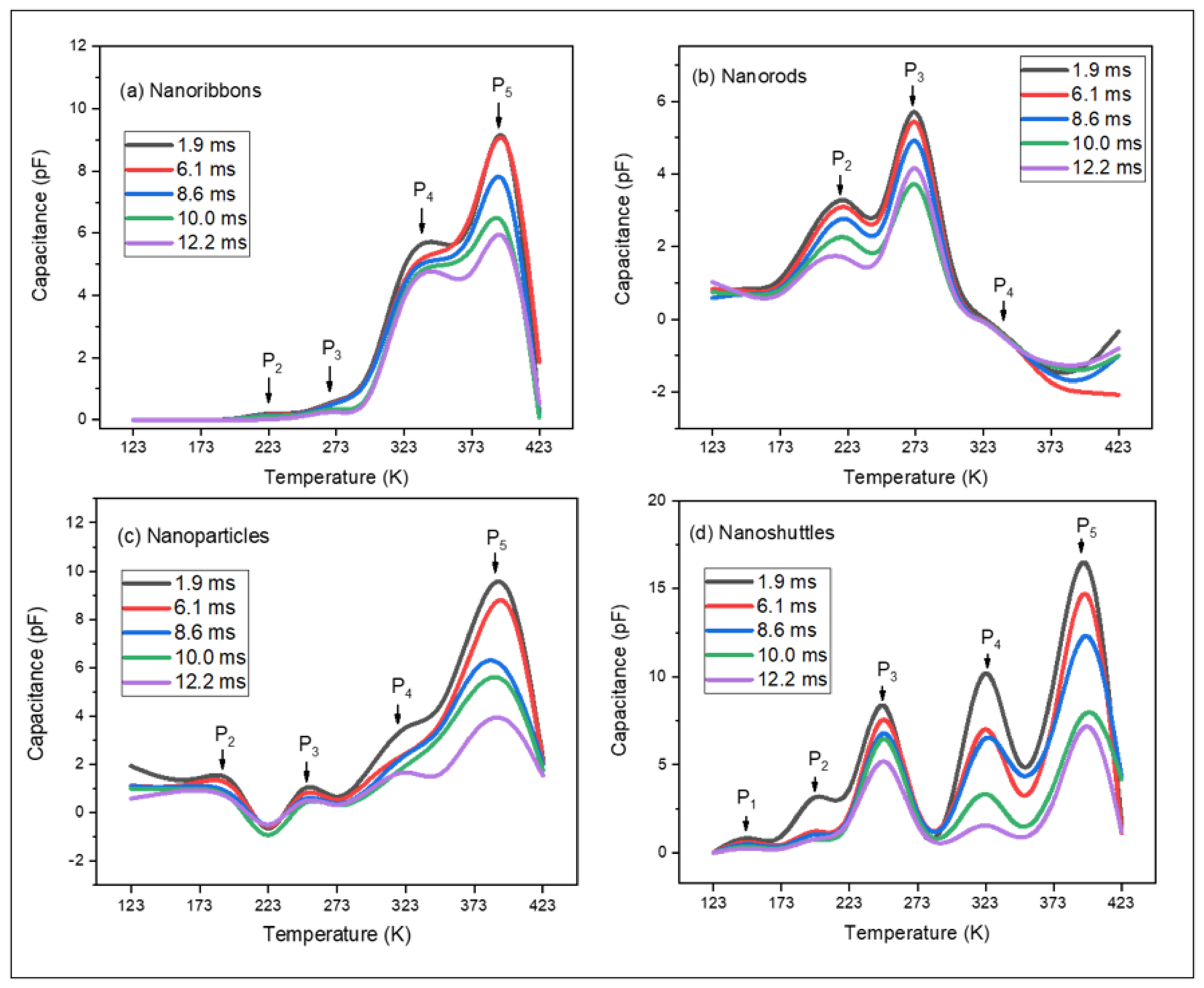
DLTS Analysis
4. Discussion
5. Conclusions
Author Contributions
Funding
Institutional Review Board Statement
Informed Consent Statement
Data Availability Statement
Acknowledgments
Conflicts of Interest
References
- Willander, M.; Nur, O.; Zhao, Q.; Yang, L.; Lorenz, M.; Cao, B.; Pérez, Z.J.; Czekalla, C.; Zimmermann, G.; Grundmann, M.; et al. Zinc oxide nanorod based photonic devices: Recent progress in growth, light emitting diodes and lasers. Nanotechnology 2009, 20, 332001. [Google Scholar] [CrossRef] [PubMed]
- Özgür, Ü.; Ya, I.; Liu, C.; Teke, A.; Reshchikov, M.; Doğan, S.; Avrutin, V.; Cho, S.-J.; Morkoç, H.A. comprehensive review of ZnO materials and devices. J. Appl. Phys. 2005, 98, 11. [Google Scholar] [CrossRef]
- Jia, Z.; Peng, K.-K.; Li, Y.-H.; Zhu, R.-S. Preparation and photocatalytic performance of porous ZnO microrods loaded with A. Trans. Nonferrous Met. 2012, 22, 873–878. [Google Scholar] [CrossRef]
- Vu Anh, T.; Pham, T.A.T.; Mac, V.H.; Nguyen, T.H. Facile controlling of the physical properties of zinc oxide and its application to enhanced photocatalysis. J. Anal. Chem. 2021, 2021, 5533734. [Google Scholar] [CrossRef] [PubMed]
- Thangeeswari, T.; George, A.T.; Kumar, A.A. Optical properties and FTIR studies of cobalt doped ZnO nanoparticles by simple solution method. Indian J. Sci. Technol. 2016, 9, 4. [Google Scholar] [CrossRef]
- Talam, S.; Karumuri, S.R.; Gunnam, N. Synthesis, characterization, and spectroscopic properties of ZnO nanoparticles. Int. Sch. Res. Not. 2012, 2012, 372505. [Google Scholar] [CrossRef]
- Pathak, T.K.; Kumar, V.; Swart, H.C.; Purohit, L.P. Electrical and optical properties of p-type codoped ZnO thin films prepared by spin coating technique. Phys. E Low Dimens. Syst. Nanostruct. 2016, 77, 1–6. [Google Scholar] [CrossRef]
- Norton, D.P.; Heo, Y.W.; Ivill, M.P.; Ip, K.; Pearton, S.J.; Chisholm, M.F.; Steiner, T. ZnO: Growth, doping & processing. Mater. Today 2004, 7, 34–40. [Google Scholar]
- Rathnasekara, R.; Hari, P. Impedance spectroscopy of nanostructured ZnO morphologies. J. Mater. Res. 2021, 36, 1937–1947. [Google Scholar] [CrossRef]
- Singh, N.; Pandey, P.; Haque, F.Z. Effect of heat and time-period on the growth of ZnO nanorods by sol-gel technique. Optik 2012, 123, 1340–1342. [Google Scholar] [CrossRef]
- Gu, C.; Huang, J.; Wu, Y.; Zhai, M.; Sun, Y.; Liu, J. Preparation of porous flower-like ZnO nanostructures and their gas-sensing property. J. Alloy. Compd. 2011, 509, 4499–4504. [Google Scholar] [CrossRef]
- Yang, F.; Liu, W.-H.; Wang, X.-W.; Zheng, J.; Shi, R.-Y.; Zhao, H.; Yang, H.-Q. Controllable low-temperature vapor-solid growth and hexagonal disk enhanced field emission property of ZnO nanorod arrays and hexagonal nanodisk networks. ACS Appl. Mater. Interfaces 2012, 4, 3852–3859. [Google Scholar] [CrossRef]
- Ding, J.; Fang, X.; Yang, R.; Kan, B.; Li, X.; Yuan, N. Transformation of ZnO polycrystalline sheets into hexagon-like mesocrystalline ZnO rods (tubes) under ultrasonic vibration. Nanoscale Res. Lett 2014, 9, 214. [Google Scholar] [CrossRef]
- Seomoon, K.; Lee, J.; Jang, P.; Jung, C.; Kim, K.-H. Synthesis and characterization of ZnO thin films deposited via PE-MOCVD. Curr. Appl. Phys. 2011, 9, S26–S29. [Google Scholar] [CrossRef]
- Siddiqui, J.; Cagin, E.; Chen, D.; Phillips, J.D. ZnO thin-film transistors with polycrystalline (Ba, Sr) TiO3 gate insulators. Appl. Phys. Lett. 2006, 88, 212903. [Google Scholar] [CrossRef]
- Chen, L.-Y.; Chen, W.-H.; Wang, J.-J.; Hong, F.C.-N.; Su, Y.-K. Hydrogen-doped high conductivity ZnO films deposited by radio-frequency magnetron sputtering. Appl. Phys. Lett. 2004, 85, 5628–5630. [Google Scholar] [CrossRef]
- Chabane, L.; Zebbar, N.; Kechouane, M.; Aida, M.S.; Trari, M. Al-doped and in-doped ZnO thin films in heterojunctions with silicon. Thin Solid Film. 2016, 605, 57–63. [Google Scholar] [CrossRef]
- Arif, M.; Shkir, M.; AlFaify, S.; Ganesh, V.; Sanger, A.; Algarni, H.; Vilarinho, P.M.; Singh, A. A structural, morphological, linear, and nonlinear optical spectroscopic studies of nanostructured Al-doped ZnO thin films: An effect of Al concentrations. J. Mater. Res. 2019, 34, 1309–1317. [Google Scholar] [CrossRef]
- Kawakami, M.; Hartanto, A.B.; Nakata, Y.; Okada, T. Synthesis of ZnO nanorods by nanoparticle assisted pulsed-laser deposition. Jpn. J. Appl. Phys. 2003, 42, L33. [Google Scholar] [CrossRef]
- Prete, P.; Lovergine, N.; Tapfer, L. Nanostructure size evolution during Au-catalysed growth by carbo-thermal evaporation of well-aligned ZnO nanowires on (100) Si. Appl. Phys. A 2007, 88, 21–26. [Google Scholar] [CrossRef]
- Nakanishi, Y.; Miyake, A.; Kominami, H.; Aoki, T.; Hatanaka, Y.; Shimaoka, G. Preparation of ZnO thin films for high-resolution field emission display by electron beam evaporation. Appl. Surf. Sci. 1999, 142, 233–236. [Google Scholar] [CrossRef]
- Liang, J.K.; Su, H.L.; Kuo, C.L.; Kao, S.P.; Cui, J.W.; Wu, Y.C.; Huang, J.C.A. Structural, optical and electrical properties of electrodeposited Sb-doped ZnO nanorod arrays. Electrochim. Acta 2014, 125, 124–132. [Google Scholar] [CrossRef]
- Wang, H.; Xie, J.; Yan, K.; Duan, M. Growth mechanism of different morphologies of ZnO crystals prepared by hydrothermal method. J. Mater. Sci. Technol. 2011, 27, 153–158. [Google Scholar] [CrossRef]
- Miccoli, I.; Spampinato, R.; Marzo, F.; Prete, P.; Lovergine, N. DC-magnetron sputtering of ZnO: Al films on (00.1) Al2O3 substrates from slip-casting sintered ceramic targets. Appl. Surf. Science. 2014, 313, 418–423. [Google Scholar] [CrossRef]
- Htay, M.T.; Hashimoto, Y.; Ito, K. Growth of ZnO submicron single-crystalline platelets, wires, and rods by ultrasonic spray pyrolysis. J. Appl. Phys. 2007, 46, 440. [Google Scholar] [CrossRef]
- Topoglidis, E.; Cass, A.E.G.; O’Regan, B.; Durrant, J.R. Immobilisation and bioelectrochemistry of proteins on nanoporous TiO2 and ZnO films. J. Electroanal. Chem. 2001, 517, 20–27. [Google Scholar] [CrossRef]
- Cheng, X.L.; Zhao, H.; Huo, L.H.; Gao, S.; Zhao, J.G. ZnO nanoparticulate thin film: Preparation, characterization and gas-sensing property. Sens. Actuators B Chem. 2004, 102, 248–252. [Google Scholar] [CrossRef]
- Hames, Y.; Alpaslan, Z.; Kösemen, A.; San, S.E.; Yerli, Y. Electrochemically grown ZnO nanorods for hybrid solar cell applications. Sol. Energy 2010, 84, 426–431. [Google Scholar] [CrossRef]
- Adhyapak, P.V.; Meshram, S.P.; Mulla, I.S.; Pardeshi, S.K.; Amalnerkar, D.P. Materials Science in Semiconductor Processing Controlled synthesis of zinc oxide nanoflowers by succinate-assisted hydrothermal route and their morphology-dependent photocatalytic performance. Mater. Sci. Semicond. Process 2014, 46, 197–206. [Google Scholar] [CrossRef]
- Lenz, T.; Richter, M.; Matt, G.J.; Luechinger, N.A.; Halim, S.C.; Heiss, W.; Brabec, C.J. Charge transport in nanoparticular thin films of zinc oxide and aluminum-doped zinc oxide. J. Mater. Chem. C. 2015, 3, 1468–1472. [Google Scholar] [CrossRef]
- Keis, K.; Bauer, C.; Boschloo, G.; Hagfeldt, A.; Westermark, K.; Rensmo, H.; Siegbahn, H. Nanostructured ZnO electrodes for dye-sensitized solar cell applications. Photochem. Photobiol. A 2002, 148, 57–64. [Google Scholar] [CrossRef]
- Singh, S.; Kumar, Y.; Kumar, H.; Vyas, S.; Periasamy, C.; Chakrabarti, P.; Jit, S.; Park, S.-H. A study of hydrothermally grown ZnO nanorod-based metal-semiconductor-metal UV detectors on glass substrates. Nanomater. Nanotechnol. 2017, 7, 1847980417702144. [Google Scholar] [CrossRef]
- Rathnasekara, R.; Hari, P. Enhancing the Efficiency of Dye-Sensitized Solar Cells (DSSCs) by Nanostructured Ag-doped ZnO Electrodes. ChemistrySelect 2022, 98, e202200830. [Google Scholar] [CrossRef]
- Peaker, A.R.; Markevich, V.P.; Coutinho, J. Tutorial: Junction spectroscopy techniques and deep-level defects in semiconductors. J. Appl. Phys. 2018, 123, 161559. [Google Scholar] [CrossRef]
- Ayoub, I.; Kumar, V.; Abolhassani, R.; Sehgal, R.; Sharma, V.; Sehgal, R.; Swart, H.C.; Mishra, Y.K. Advances in ZnO: Manipulation of defects for enhancing their technological potentials. Nanotechnol. Rev. 2022, 11, 575–619. [Google Scholar] [CrossRef]
- Vanheusden, K.; Seager, C.H.; Warren, W.L.T.; Tallant, D.R.; Voigt, J.A. Correlation between photoluminescence and oxygen vacancies in ZnO phosphors. Appl. Phys. Lett 1996, 68, 403–405. [Google Scholar] [CrossRef]
- Lang, D.V. Deep-level transient spectroscopy: A new method to characterize traps in semiconductors. J. Appl. Phys. 1974, 45, 3023–3032. [Google Scholar] [CrossRef]
- Wenckstern, V.H.; Pickenhain, R.; Schmidt, H.; Brandt, M.; Biehne, G.; Lorenz, M.; Grundmann, M.; Brauer, G. Deep acceptor states in ZnO single crystals. Appl. Phys. Lett. 2006, 89, 092122. [Google Scholar] [CrossRef]
- Simpson, J.C.; Cordaro, J.F. Characterization of deep levels in zinc oxide. J. Appl. Phys. 1988, 63, 1781–1783. [Google Scholar] [CrossRef]
- Auret, F.D.; Goodman, S.A.; Hayes, M.; Legodi, M.J.; Van Laarhoven, H.A.; Look, D.C. Electrical characterization of 1.8 MeV proton-bombarded ZnO. Appl. Phys. Lett. 2001, 79, 3074–3076. [Google Scholar] [CrossRef]
- Auret, F.D.; Nel, J.M.; Hayes, M.; Wu, L.; Wesch, W.; Wendler, E. Electrical characterization of growth-induced defects in bulk-grown ZnO. Superlattices Microstruct. 2006, 39, 17–23. [Google Scholar] [CrossRef]
- Cordaro, J.F.; Shim, Y.; May, J.E. Bulk electron traps in zinc oxide varistors. J. Appl. Phys. 1986, 60, 4186–4190. [Google Scholar] [CrossRef]
- Chiou, B.-S.; Chung, M.-C. Admittance spectroscopy and trapping phenomena of ZnO based varistors. Electron. Mater. 1991, 20, 885–890. [Google Scholar] [CrossRef]
- Blatter, G.; Greuter, F. Electrical Properties of Grain Boundaries in Polycrystalline Compound Ceramics. Semicond. Sci. Technol. 1990, 5, 111–137. [Google Scholar]
- Frenzel, H.; Wenckstern, H.V.; Weber, A.; Schmidt, H.; Biehne, G.; Hochmuth, H.; Lorenz, M.; Grundmann, M. Photocurrent spectroscopy of deep levels in ZnO thin films. Phys. Rev. B 2007, 76, 035214. [Google Scholar] [CrossRef]
- Zhao, X.; Li, J.; Li, H.; Li, S. Intrinsic and extrinsic defect relaxation behavior of ZnO ceramics. J. Appl. Phys. 2012, 111, 124106. [Google Scholar] [CrossRef]
- Paradowska, K.M.; Płaczek-Popko, E.; Pietrzyk, M.A.; Gwóźdź, K. Kozanecki, A. Current transport and deep levels in p-Si/n-Zn0.9Mg0.1O/n-ZnO heterojunction. J. Alloy. Compd. 2017, 691, 946–951. [Google Scholar] [CrossRef]
- Polyakov, A.Y.; Smirnov, N.B.; Govorkov, A.V.; Kozhukhova, E.A.; Belogorokhov, A.I.; Norton, D.P.; Kim, H.S.; Pearton, S.J. Shallow and deep centers in as-grown and annealed MgZnO/ZnO structures with quantum wells. J. Electron. Mater. 2010, 39, 601–607. [Google Scholar] [CrossRef]
- Auret, F.D.; Goodman, S.A.; Legodi, M.J.; Meyer, W.E.; Look, D.C. Electrical characterization of vapor-phase-grown single-crystal ZnO. Appl. Phys. Lett. 2002, 80, 1340–1342. [Google Scholar] [CrossRef]
- Oh, D.C.; Suzuki, T.; Kim, J.J.; Makino, H.; Hanada, T.; Cho, M.W.; Yao, T. Electron-trap centers in ZnO layers grown by molecular-beam epitaxy. Appl. Phys. Lett. 2005, 86, 032909. [Google Scholar] [CrossRef]
- Quemener, V.; Vines, L.; Monakhov, E.V.; Svensson, B.G. Evolution of deep electronic states in ZnO during heat treatment in oxygen-and zinc-rich ambients. Appl. Phys. Lett. 2012, 100, 112108. [Google Scholar] [CrossRef]
- Look, D.C.; Reynolds, D.C.; Sizelove, J.R.; Jones, R.L.; Litton, C.W.; Cantwell, G.; Harsch, W.C. Electrical properties of bulk ZnO. Solid State Commun. 1998, 105, 399–401. [Google Scholar] [CrossRef]
- Vempati, S.; Mitra, J.; Dawson, P. One-step synthesis of ZnO nanosheets: A blue-white fluorophore. Nanoscale Res. Lett. 2012, 7, 470. [Google Scholar] [CrossRef] [PubMed]
- Wen, X.; Zhang, Q.; Shao, Z. Magnetron sputtering for ZnO: Ga scintillation film production and its application research status in nuclear detection. Crystals 2019, 9, 263. [Google Scholar] [CrossRef]
- Bylander, E.G. Surface effects on the low-energy cathodoluminescence of zinc oxide. J. Appl. Phys. 1978, 49, 1188–1195. [Google Scholar] [CrossRef]
- Hagemark, K.I.; Chacka, L.C. Electrical transport properties of Zn doped ZnO. J. Appl. Phys. 1975, 15, 261–270. [Google Scholar] [CrossRef]
- Choi, J.S.; Yo, C.H. Study of the nonstoichiometric composition op zinc oxide. J. Phys. Chem. Solids 1976, 37, 1149–1151. [Google Scholar] [CrossRef]
- Rohatgi, A.; Pang, S.K.; Gupta, T.K.; Straub, W.D. The deep level transient spectroscopy studies of a ZnO varistor as a function of annealing. J. Appl. Phys. 1988, 63, 5375–5379. [Google Scholar] [CrossRef]
- Tapan, K.G.; William, G.C. Barrier voltage and its effect on stability of ZnO varistor. J. Appl. Phys. 1982, 53, 7401–7409. [Google Scholar]
- Fan, J.; Zhang, Z.; Tian, H.; Zhao, H.; Freer, R. Investigation of the effect of different dopants on the trap states of ZnO-based and SnO2-based varistors. J. Phys. Conf. Ser. 2009, 152, 012060. [Google Scholar] [CrossRef]
- Vines, L.; Monakhov, E.V.; Svensson, B.G. Effect of high-temperature treatments on defect centers and impurities in hydrothermally grown ZnO. Phys. B Condens. 2009, 404, 4386–4388. [Google Scholar] [CrossRef]
- Chicot, G.; Pernot, J.; Santailler, J.-L.; Chevalier, C.; Granier, C.; Ferret, P.; Ribeaud, A.; Feuillet, G.; Muret, P. Electronic properties of E3 electron trap in n-type ZnO. Phys. Status Solidi B 2014, 251, 206–210. [Google Scholar] [CrossRef]
- Vehse, W.E.; Sibley, W.A.; Keller, F.J.; Chen, Y. Radiation damage in ZnO single crystals. Phys. Rev. 1968, 167, 828. [Google Scholar] [CrossRef]
- Polyakov, A.Y.; Smirnov, N.B.; Govorkov, A.V.; Kozhukhova, E.A.; Pearton, S.J.; Norton, D.P.; Osinsky, A.; Dabiran, A. Electrical properties of undoped bulk ZnO substrates. J. Electron. Mater. 2006, 35, 663–669. [Google Scholar] [CrossRef]
- Ullattil, S.G.; Jabeen, F.M.J.; Abdel-Wahab, A. Defect minimized Ag-ZnO microneedles for photocatalysis. Environ. Sci. Pollut. Res. 2020, 27, 37036–37043. [Google Scholar] [CrossRef] [PubMed]
- Selim, F.A.; Weber, M.H.; Solodovnikov, D.; Lynn, K.G. Nature of native defects in ZnO. Phys. Rev. Lett. 2007, 8, 085502. [Google Scholar] [CrossRef] [PubMed]
- Cao, B.; Cai, W.; Zeng, H. Temperature-dependent shifts of three emission bands for ZnO nanoneedle arrays. Appl. Phys. Lett. 2006, 88, 161101. [Google Scholar] [CrossRef]
- Chai, J.; Mendelsberg, R.J.; Reeves, R.J.; Kennedy, J.; Von, W.H.; Schmidt, M.; Grundmann, M.; Doyle, K.; Myers, T.H.; Durbin, S.M. Identification of a deep acceptor level in ZnO due to silver doping. J. Electron. Mater. 2010, 39, 577–583. [Google Scholar] [CrossRef]
- Allen, M.W.; Durbin, S.M. Influence of oxygen vacancies on Schottky contacts to ZnO. Appl. Phys. Lett. 2008, 92, 122110. [Google Scholar] [CrossRef]
- Hisham, H. Characterization Methods for Submicron MOSFETs; Springer Science & Business Media: Berlin/Heidelberg, Germany, 2012; Volume 352. [Google Scholar]
- Scheffler, L.; Kolkovsky, V.l.; Lavrov, E.V.; Weber, J. Deep level transient spectroscopy studies of n-type ZnO single crystals grown by different techniques. J. Condens. Matter Phys. 2011, 23, 334208. [Google Scholar] [CrossRef]
- Ci-Hui, L.; Bing-Ce, L.; Zhu-Xi, F. Electrical and deep levels characteristics of ZnO/Si heterostructure by MOCVD deposition. Chin. Phys. B 2008, 17, 2292. [Google Scholar] [CrossRef]
- Von, W.H.; Biehne, G.; Lorenz, M.; Grundmann, M.; Auret, F.D.; Meyer, W.E.; van, R.P.J.J.; Hayes, M.; Nel, J.M. Dependence of trap concentrations in ZnO thin films on annealing conditions. J. Korean Phys. Soc. 2008, 53, 2861–2863. [Google Scholar]
- Wu, X.L.; Siu, G.G.; Fu, C.L.; Ong, H.C. Photoluminescence and cathodoluminescence studies of stoichiometric and oxygen-deficient ZnO films. Appl. Phys. Lett. 2001, 78, 2285–2287. [Google Scholar] [CrossRef]


| Nano Structure Name | Trap | T (K) | Ea (eV) | α (cm2) |
|---|---|---|---|---|
| Nanoribbons | P2 | 220 | 0.31 ± 0.01 | (1.49 ± 0.12) × 10−15 |
| P3 | 273 | 0.23 ± 0.01 | (2.02 ± 0.81) × 10−18 | |
| P4 | 333 | 0.87 ± 0.02 | (4.80 ± 1.02) × 10−11 | |
| P5 | 395 | 0.44 ± 0.03 | (6.09 ± 0.31) × 10−18 | |
| Nanorods | P2 | 218 | 0.27 ± 0.01 | (2.79 ± 0.91) × 10−16 |
| P3 | 270 | 0.18 ± 0.01 | (1.18 ± 1.05) × 10−18 | |
| P4 | 333 | 0.75 ± 0.04 | (4.59 ± 1.31) × 10−11 | |
| Nanoparticles | P2 | 190 | 0.28 ± 0.02 | (2.83 ± 0.51) × 10−15 |
| P3 | 250 | 0.22 ± 0.01 | (7.09 ± 1.35) × 10−17 | |
| P4 | 320 | 0.88 ± 0.03 | (9.49 ± 0.75) × 10−11 | |
| P5 | 386 | 0.51 ± 0.02 | (2.25 ± 0.67)× 10−16 | |
| Nanoshuttle | P1 | 145 | 0.13 ± 0.01 | (1.03 ± 0.64) × 10−17 |
| P2 | 190 | 0.28 ± 0.02 | (9.48 ± 0.68) × 10−15 | |
| P3 | 248 | 0.25 ± 0.01 | (1.67 ± 0.31) × 10−17 | |
| P4 | 322 | 0.94 ± 0.01 | (7.07 ± 1.36) × 10−11 | |
| P5 | 397 | 0.50 ± 0.03 | (2.89 ± 1.41) × 10−16 |
Disclaimer/Publisher’s Note: The statements, opinions and data contained in all publications are solely those of the individual author(s) and contributor(s) and not of MDPI and/or the editor(s). MDPI and/or the editor(s) disclaim responsibility for any injury to people or property resulting from any ideas, methods, instructions or products referred to in the content. |
© 2024 by the authors. Licensee MDPI, Basel, Switzerland. This article is an open access article distributed under the terms and conditions of the Creative Commons Attribution (CC BY) license (https://creativecommons.org/licenses/by/4.0/).
Share and Cite
Rathnasekara, R.; Mayberry, G.M.; Hari, P. Deep-Level Transient Spectroscopy Studies on Four Different Zinc Oxide Morphologies. Crystals 2024, 14, 224. https://doi.org/10.3390/cryst14030224
Rathnasekara R, Mayberry GM, Hari P. Deep-Level Transient Spectroscopy Studies on Four Different Zinc Oxide Morphologies. Crystals. 2024; 14(3):224. https://doi.org/10.3390/cryst14030224
Chicago/Turabian StyleRathnasekara, Rusiri, Grant M. Mayberry, and Parameswar Hari. 2024. "Deep-Level Transient Spectroscopy Studies on Four Different Zinc Oxide Morphologies" Crystals 14, no. 3: 224. https://doi.org/10.3390/cryst14030224
APA StyleRathnasekara, R., Mayberry, G. M., & Hari, P. (2024). Deep-Level Transient Spectroscopy Studies on Four Different Zinc Oxide Morphologies. Crystals, 14(3), 224. https://doi.org/10.3390/cryst14030224