1. Introduction
The increasingly high capability and switching frequency in power electronic devices requires suitable metallization schemes, not only for electrical connection but also for dissipation of the thermal heat generated by the high power density [
1,
2]. In this respect, Cu metallization, with its increased electromigration resistivity, low resistivity (
) and high thermal conductivity (4.01 Wcm/K at 300) [
3,
4] is replacing the Al layer [
5] currently in use, actively removing the thermal energy and preventing device damaging [
3]. Furthermore, Copper front metal enables to consider Cu-Cu wire bonding, which offers alternatives to the Cu-Al or Au-Al systems.
However the application of a Cu-based metallization scheme requires an accurate control of the morphological evolution of nano- or poly-crystalline Cu film during the processing steps [
6,
7]. Indeed, despite the cited advantages, nearly room temperature electroplated copper has unstable grains, with a high density of defects such as impurities coming from bath, dislocations, and grain boundaries, which can be considered as the main source of a large amount of energy stored in the as-deposited fine grains of electroplated Cu films [
4,
5]. Therefore, the layer has to be thermally stabilized. Thermal treatment of thick Cu deposited on semiconductors’ substrates modifies the composed system at different scales. For instance, Cu in direct contact with Si can lead to relevant kinetic reaction at relatively low temperature [
8]. Moreover, micro-structural modifications in the Cu film, induced by the grain densification phenomenon, transfer a stress field in the elasto-plastic regime to the substrate [
9], which has a dramatic effect as global warpage of wafers.
A significant warpage makes power device fabrication difficult, especially if the final device thickness is lower than 100
m. Moreover, high wafer warpage causes yield loss during chip assembly and package mount on the circuit board. Strategies aimed at warpage control and optimization enabling this challenging technology are hence necessary, implying a deeper understanding of the microscopic kinetics and global mechanical behaviour of the Cu-Si and, in general, Cu-substrate systems. From the macroscopic point of view, freestanding films and films deposited to thick substrates in fact behave differently. A noticeable difference is that freestanding films can be stressed only in tension whereas films bonded to substrates with relatively low coefficients of thermal expansion can be stressed in both tension and compression by varying the temperature. Furthermore, plastic deformation in a layer-substrate system bonded is, in some way, governed by the substrate [
10].
A complete analysis of the impact of a metallization (sequence of depositions and thermal curing) to the micro- and macro-structures (metal layers, compliant interfaces, underlying substrates, global wafers) affected by the process is difficult to find in the literature. Therefore, the optimization of the processes’ conditions is usually obtained without a comprehensive study of the micro-structural evolution for “all” the crystalline materials present in the system. Moreover, the support of reliable 3D models, simulating the system kinetics with the due accuracy, also seems very necessary in this kind of investigation.
In this work we provide an innovative holistic approach to the problem, exploring the micro-structural changes in electrochemically deposited (ECD) poly-crystalline Cu films during subsequent thermal cycles at moderate maximum temperatures, suitable for integration into advanced metallization schemes for electronic device manufacturing. The alterations resulting from the thermal treatments are analysed at various scales, ranging from the film-substrate interface to the wafer scale, using complementary techniques such as X-ray Diffraction (XRD), scanning electron microscopy (SEM), atomic force microscopy (AFM), and dynamical warpage measurements. First, we investigate 20 m thick Cu layers grown by ECD on (from top to bottom) Cu 200 nm/(Ti)W 300 nm/Si substrates, highlighting the occurrence of self-annealing in the as-deposited samples, the grain densification due to thermal treatment and its impact on wafer warpage. A tri-dimensional (3D) on-cell model, based on the Pott-like multi-states configurational energy dependence, is also employed to simulate the internal grains’ evolution in the films, while accounting for multiple grain orientations and densification kinetics in the canonical ensemble. Then, we compare samples with (hereafter named “”) and without (hereafter named “”) the thick ECD-grown Cu layer on top, discussing the implications of thermal treatment on the morphology of the composite Cu/substrate system. In particular, we study how the interfacing Cu 200 nm/(Ti)W 300 nm stack mediates the interactions between the ECD-grown Cu layer and the rest of the substrate.
2. Materials and Methods
The
samples consist of 20
m thick Cu layers grown by electrochemical deposition (ECD) on Cu 200 nm/(Ti)W 300 nm/Si substrates, with commercially available ENTHONE baths in an AMAT-RAIDER equipment (Santa Clara, CA, USA). The
samples refer to the same systems but without the top Cu layer (i.e., prior to ECD). The (Ti)W and Cu 200 nm layers were sequentially PVD deposited on a (100) substrate using the AMAT-Endura-PVD system by introducing Ar in the PVD chamber and reaching the base pressure of about 7 mTorr. The sputtering power was 3.5 kW. The deposition time was 100 and 150 s, respectively, for Cu and (Ti)W. The intermediate (Ti)W layer is used as adhesion promoter layer. (Ti)W stands for a layer deposited by PVD using a TiW target with 90% wt W, 10% wt Ti. Therefore, we can consider the film as a W rich W-Ti system. The Cu 200 nm layer is a PVD deposited layer that can guarantee the
layer growth. Without this layer the
does not nucleate and grow. The thicknesses of intermediate layers were chosen to guarantee film continuity and represent a good compromise in terms of induced warpage. Bulk thermal treatment in the temperature range between 150
C and 400
C has been performed on all samples. The annealing temperature cycles were implemented with up and down ramps at constant rates while the plateau was maintained for 60 min in all the cases. Warpage measurements have been performed by means of an MX 102-204-RA-2C tool by E+H Metrology GmbH (Karlsruhe, Germany). The warpage is defined as the maximum variation between individual points on the upper side of the wafer with respect to a least squares fit plane based on these points [
11]. The stress of the as-deposited and thermally treated
and
samples has been calculated by using Stoney’s formula [
12,
13]. Morphology changes have been studied using SEM (DualBeam 865 by FEI Company, Hillsboro, OR, USA, in SEM modality) and AFM (Vx210 Atomic-Force Profiler by Veeco, Munich, Germany). Statistic of grain size distribution and evolution as a function of temperature has been obtained using several representative plan view SEM analyses. Structure and composition have been studied by X-ray Diffraction (XRD) analysis using an AXS D8 DISCOVER diffractometer by Bruker (Billerica, MA, USA) working with a Cu-K
source.
The
grain densification has been simulated by means of a cellular automata-like approach (see, e.g., Ref. [
14] and references therein) allowing a realistic description of the grains’ evolution (growth). The kinetics are simulated by means of stochastic sequences of local transitions of the “cells” of a three dimensional lattice, where the poly-crystalline structure is mapped. The single cell represents a volume portion and stores the value of the orientation variable of the volume itself. The local event promoting the nano- or poly-crystal evolution (note that the size and resolution can be properly tuned, as it depends on the elementary cell volume) is the status change of the cells which can modify their orientation, at a given time
of the evolution, to another one among the total number
of the possible ones. The corresponding transition probability (rate) is ruled by the local energy barrier
, according to the transition state theory. The “potential” transition rate is
where
is the only calibration parameter in the model and the energy barrier
is calculated by the following Pott-like [
15] lattice energy model
where
is the “orientation” of the volume in the
i-th cell,
) the grain boundary (monomer-grain) energy cost,
is the orientation of the next neighbour cell in the lattice and
is the usual discrete delta function. We note that the energy in the bulk of the grain is the reference energy since
for a cell which has all the neighbours with the same orientation.
) is a calibration function which for homogeneous materials is chosen in a way that the model recovers the correct melting transition at the melting temperature
(see
Figure 1). Moreover, by means of a fine tuning of
), an orientation penalty, epitaxial or similar interface dependent energy modification could also be effectively included in the model for future extensions. The frequency
has been chosen, aligning simulated and real kinetics in a single temperature process, then the same value is used for all the cases. Time integration in the Pott-like model is usually performed with the continuum time algorithm, which accelerates the computation [
16].
3. Results and Discussion
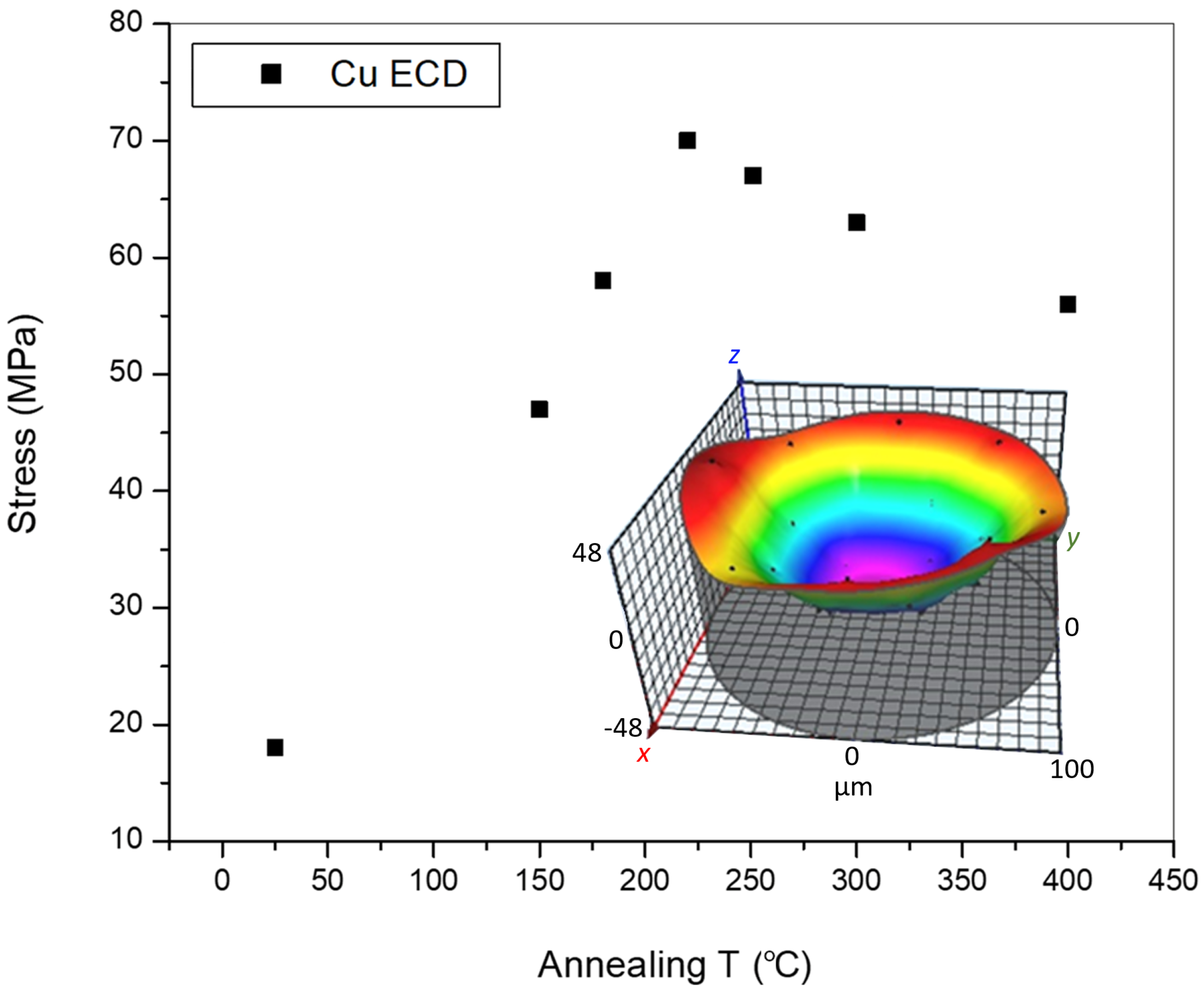
Stress values for
layers are shown in
Figure 2. The as-deposited Cu layer has a stress value of about 18 MPa. After thermal annealing at 150
C the stress value increases up to 47 MPa. Note that the Cu layer at this temperature is not stable and will evolve in terms of stress and layer morphology. Indeed, the stress value increases as a function of the annealing temperature, reaching a maximum value of 70 MPa at 220
C. At temperature values higher than 220
C the film stress decreases, reaching the minimum value of 56 MPa at 400
C. The temperature dependence of stress represents a first indication of the structural changes that the system undergoes during the thermal annealing treatment.
To get insights on these modifications at the micro-scale, we have investigated the
morphological evolution correlating microscopic analysis
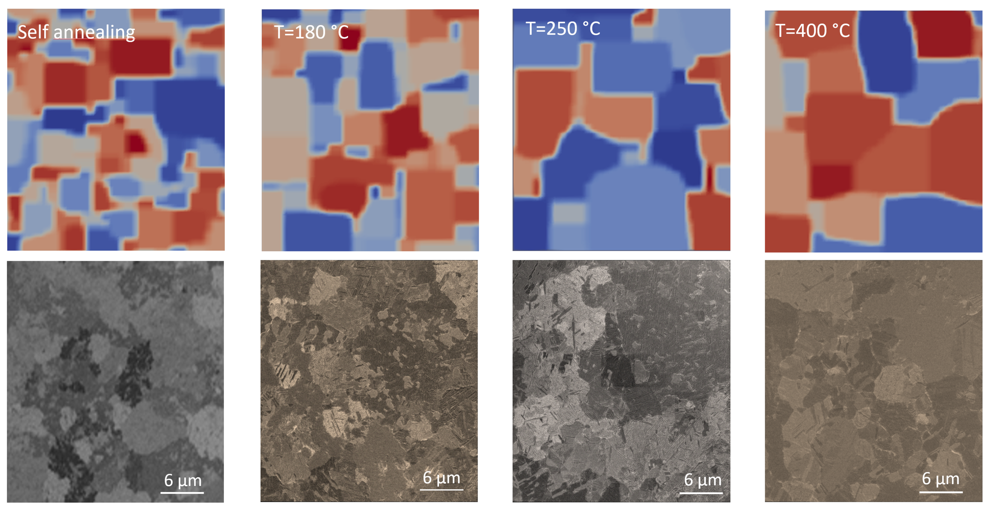
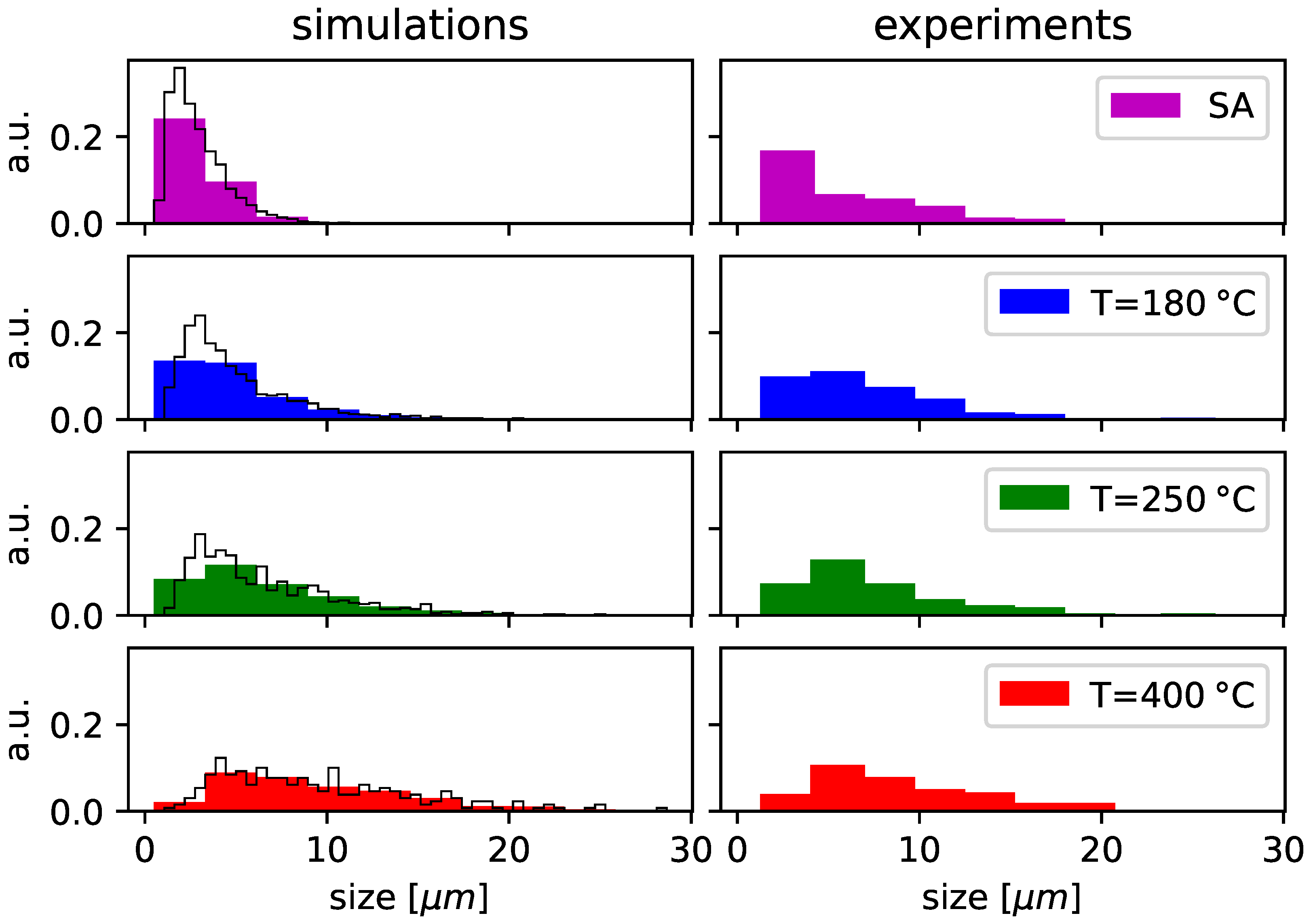
after the thermal curing and the full processes’ simulations. Plane view SEM analyses and grain size distribution of
as-deposited and thermally treated at 180
C, 250
C and 400
C are shown in
Figure 3 and
Figure 4 respectively, and compared with the simulation results. All layers are dense and there is no observable porosity or cracks on the surface. Room temperature crystallization with the appearance of relative large Cu grains, termed self-annealing (SA), occurs in as-deposited samples (
Figure 3, left side graphs). This state is reproduced in the simulation with a suitable long annealing at low T (50
C) starting from a initial totally disordered state. We notice that the self-annealed state is used as the initial one in all the simulations of the curing processes after the verification that ±20% modifications in the preparing self-annealing simulation in terms of temperature and time does not significantly affect the results of the subsequent simulated Cu curing processes. In the experimental systems, the self-annealing is instead a consequence of the deposition mode (continuous DC mode) that allows for concurrent and progressive nucleation, grain growth, and re-crystallization, while maintaining high deposition rates. This is a peculiarity of the DC mode with respect to the pulsed deposition (on-off) mode, where the grain nucleation occurs during the “on” time step whilst stress relaxation, grain growth and recrystallization occurs during the “off” time step.
Reliable considerations can be derived by integrating SEM post-process analysis with kinetic simulations. In terms of final state description, they are in a significant agreement as the comparisons of the final snapshots and grain size distributions in the
Figure 3 and
Figure 4 demonstrate. The use of the 3D simulations offers significant vantages in the study of the kinetics with respect to the theoretical scheme based on grain mean-size only [
17,
18], since the full size distribution can be properly modelled. We notice that, to align in parallel experiments and simulations, the snapshots in
Figure 3 are shown within the same space scale and the statistical analysis in
Figure 4 are performed with the same bin intervals of 2.25
m width (coloured bars in left and right columns of
Figure 4). The simulations are performed in a rather large simulation box (
) and the analysis can be extended in the whole three dimensional film structure, allowing for a more refined statistic of the size distribution (i.e., with a smaller bin), as the ones shown (with 0.45
m bins’ width) with the black line contours of the bars in the graphs reported in the left column of
Figure 4. We notice that the combination of structural analysis and simulations indicates that, in spite of the non monotonic behaviour as a function of the temperature shown in
Figure 2, the Cu grain densification occurring at the micro-scale drives the stress behaviour at the wafer-level. The impact of the temperature on the ripening phenomenon is clearly evidenced by the simulations and validated by the experimental data. The driving force for the ripening is the reduction of the grain boundaries, due to their energetic cost with respect to the bulk, with a consequent global contraction of the film, no additional modification to the Pott model formulation is necessary to recover the experimental scenario. The simulations calculate a final reduction of the grain boundary volume of 55%, 41%, and 27% for the 180
C, 250
C, and 400
C cases respectively with respect to the self-annealed post deposition state.
SEM microscopy shows that in thermally treated samples the huge increase in grain size and the induced deformation are associated with the formation of twin defects that are clearly visible for the three annealing temperatures (see, e.g., the arrows in
Figure 3). Since no evidence of twinning has been detected on self-annealed samples, the twinning formation can be considered as a consequence of micro-state modification induced by the thermal treatment in our samples. This plastic release of the densification induced stress has also been reported by Simoes et al. [
19] who observed the microstructural evolution of Cu grains during in situ annealing and showed that twins form inside a Cu grain, which grows extensively at the expense of other small grains.
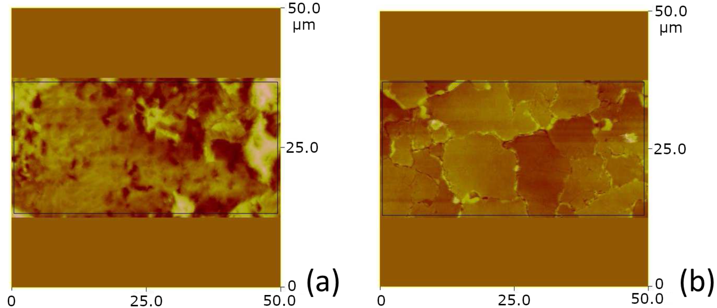
Despite the similar grain size distribution, the layers exhibit quite a different surface roughness, such as the Rq value of 95 nm in case of annealing at 250
C and of 28 nm in case of annealing at 400
C (
Figure 5). Another important feature highlighted by the AFM analysis is the Cu grain boundary, which appears well defined in the surface height map measurement only in case of annealing at 400
C.
While the grain evolution leads to a reduction of the grain boundary volume, which increases with the temperature, the stress trend in
Figure 2 seems to indicate an important role of the Cu-film/Si-substrate interface. We have tried to understand the relationship between film evolution and global stress, investigating the micro-structural modifications of the interface stack without the presence of the 20
m thick Cu film.
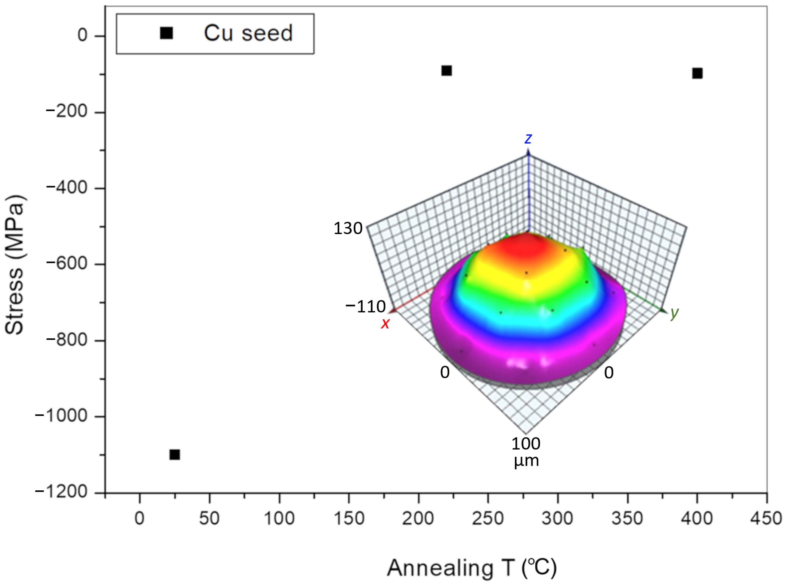
Figure 6 shows stress values as a function of temperature for
samples. The data are a mean value over several wafers intending to test process reproducibility. The deposited layers exhibit a quite large compressive stress of about −1.1 GPa. After thermal treatment, the stress values dramatically decreases down to −0.1 GPa with only slight changes as a function of annealing temperature. The figures on the inset report a wafer shape as obtained by the curvature measurement.
Plan view SEM analyses and grain size distribution of
as-deposited and thermally treated samples at 250
C and 400
C are shown in
Figure 7. Pictures captured after
deposition reveal a fine grained structure (
Figure 7a) with the total frequency of grains at the side of the smaller dimension of the distribution: the grain dimensions not exceeding 200 nm and the median value being 100 nm (
Figure 7b). After thermal treatment at 250 C grains with regular, square shaped faces with rounded edges start to appear (
Figure 7c). These faces, oriented in various directions, extend deeper into the surface, creating a cube-like pattern. The grain count dramatically decreases, the size distribution assuming a unimodal aspect (
Figure 7d). An increase in median grain size up to 200 nm has been measured in this case. Only residual fine Cu seed grains can be appreciated at an annealing temperature of 400
C (
Figure 7e). Histogram populates towards the high grain dimension with an appearance of a bimodal distribution.
Surface roughness changes on a 10×10
area are shown in
Figure 8. An almost flat surface with Rq = 3.5 nm has been found on the as-deposited samples (
Figure 8a). After the thermal treatment, the Rq value increases to 18 nm in the case of 250
C (
Figure 8b) and 20 nm in the case on 400
C (
Figure 8c).
To identify the structural modification that both
and
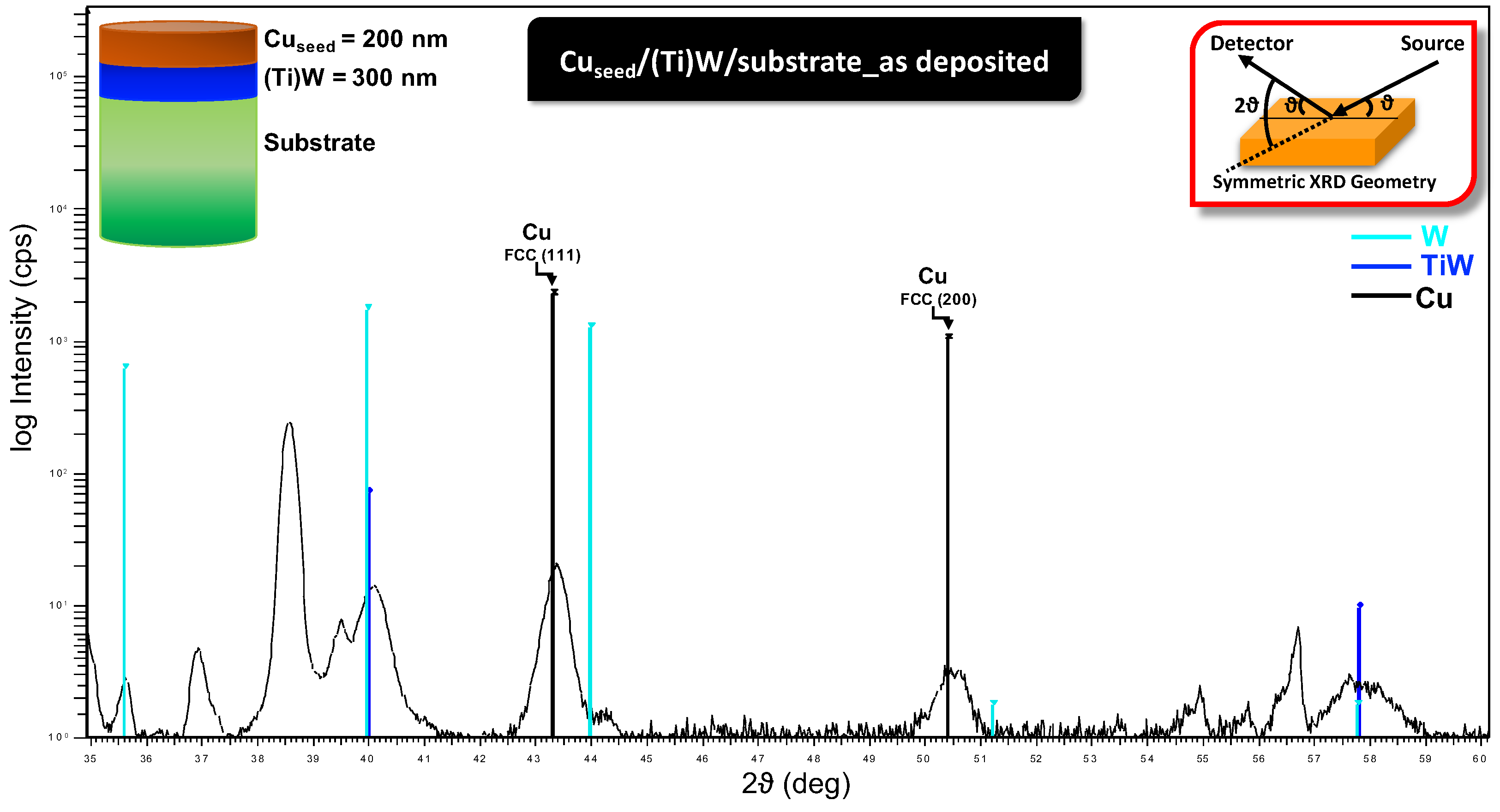
samples undergo after thermal treatment at different temperatures, XRD analyses have been done in symmetric XRD configuration (see the top right inset of
Figure 9). The XRD pattern of the entire
sample in as-deposited conditions is shown in
Figure 9. We can observe the different contributions of W (light blue line), (Ti)W (blue line), Cu (black line), and the other peaks related to the substrate. The schematic reported in the inset on the top left shows the sample structure, where we can observe the details regarding the layers’ thickness. Concerning the Cu contributions, we found two out of the three main peaks of the Face-Cubic Centred (FCC) lattice, i.e., the (111) at 2
= 43.35
and the (200) at 2
= 50.48
. We note that other FCC peaks might exist outside the range of XRD angles explored in this work (i.e., 35–60
).
The
sample has also been treated at different temperatures, i.e., at 250
C and 400
C, respectively. The purpose of these treatments was to verify how the temperature influences two important issues: (1) the improvement of the structural order and (2) a preferential orientation between the two Cu main peaks.
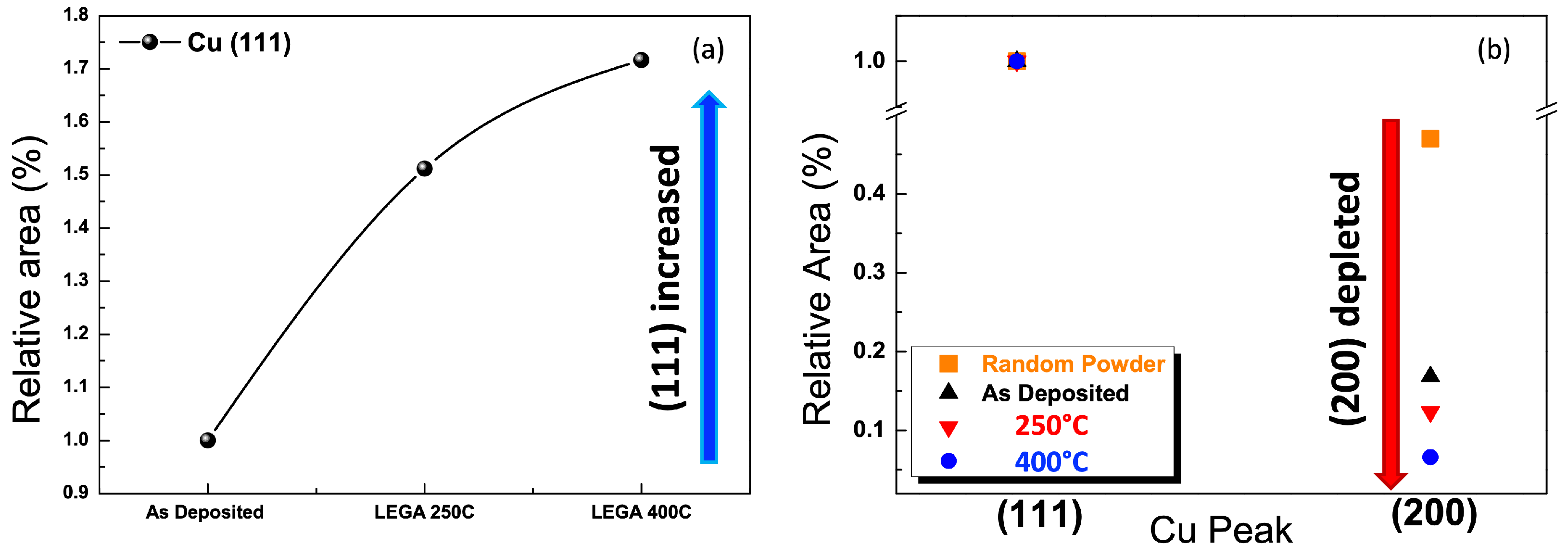
Figure 10a shows the normalized area trend of the (111) Cu peak after thermal treatment at 250
C and 400
C compared to the as-deposited condition. The values increase with temperature, indicating an improvement of the structural order regarding the (111) Cu planes for the samples where the thermal budget was applied.
In order to have a complete scenario in terms of the structural properties for the Cu main peaks, we compared the relative area of the Cu (111) and (200) peaks with the Cu random powder sample as a reference. We found that the relative area ratio between the (111) and (200) Cu planes for each sample gradually decreased with increasing temperature (see
Figure 10b).
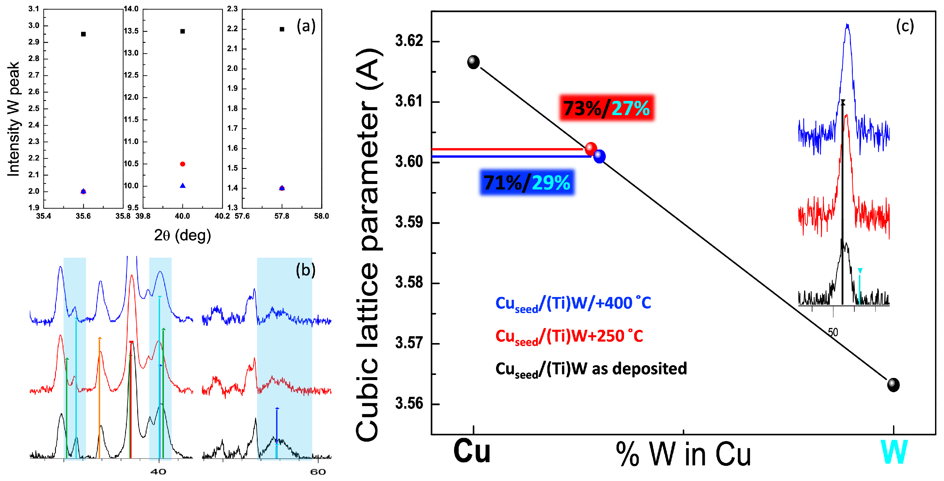
Figure 11a shows the XRD patterns, in the range 2
= 34–59
, for the
samples in as-deposited conditions and with a thermal treatment both at 250
C and at 400
C. Here, we highlight with light blue the W peaks related to the (200), (210), and (310) planes located at the 2
= 35.59
, 2
= 39.97
and 2
= 57.81
, respectively. The intensity trend of each peak in the three different conditions is reported in
Figure 11b, where an intensity lowering is evident for all W peaks in the annealed samples. In particular, for the (200) and (310) W planes, the relative intensity value is the same for both
samples treated at 250
C and at 400
C. On the other hand, for the W peak related to the (210) plane, we found a small difference between the two thermal budgets, likely because this plane is less sensitive to a soft thermal budget like 250
C. Further details of the relative differences of the W peaks are shown in
Table 1.
Figure 11c shows a Vegard plot focused on the XRD peak at 2
= 50.45
(see inset). Following Vegard’s law, if we assume that the lattice parameter of a Cu/W binary system changes linearly between the pure Cu and pure W lattice parameters, we can estimate the %W dispersion in the Cu matrix. Using this approach, we estimated the %W dispersed inside the Cu matrix for both
samples thermally treated at 250
C and 400
C:
Hence, we found an increase in %W within the Cu matrix after temperature annealing, which facilitates the dilution of W. It is worth noting that, although W and C are thermodynamically immiscible [
20], our findings support the formation of Cu-W pseudo-alloy [
21]. Indeed, diffusion and mixing phenomena occurring in thin film systems could lead to a metastable state that deviates from the equilibrium phase diagram.
To complete our structural analysis, we compared the
and
samples. This final study was useful to understand if the two kinds of samples show different behaviours in terms of structural properties regarding the two Cu main peaks, i.e., the (111) and (200), respectively.
Figure 12 schematically shows the analogies between the two samples concerning the lattice spacing (
) and the crystalline size. The detailed data are reported in
Table 2. After the thermal treatment, both samples show a similar behaviour, despite the differences in terms of thickness and morphology.
4. Conclusions
The evolution of the electronic devices is guided by their functional design, which indicates new specifications for the sub-components of the device system. In the case of metal layers, new specifications could impact the feasibility of the processes’ integration at different levels (scales), due to the modifications with respect to the standard necessary to obtain the desired results. Indeed, the metal deposition and the eventual further thermal curing could impact both the semiconductor micro- and nano-structures (inducing damage) and the subsequent processing (due, e.g., to an excessive global warpage of the wafer). Material science studies, eventually supported by process simulation, are necessary to deeply understand the phenomena involved in the process and speed up the integration procedure, also gaining predictive potential for future application of the methods in continuum improvement of the device performances.
In the present work, by combining several structural characterization techniques and in-cell 3D simulations, we have thoroughly investigated a process sequence aimed at increasing the ECD Cu film thickness with respect to those used in a previous device technology. Our results on the complete multi-layer stack indicate that the driving force for the micro-structural evolution during the thermal cycle is the increase in grain size induced by a grain boundary-mediated ripening phenomenon. The simulations based on a properly calibrated Pott-like model predict with a good accuracy the internal kinetics of the poly-crystalline film for all the studied cases. Therefore, they represent a reliable tool for supporting the process development in different conditions and geometries.
Comparing the stress measurements at the wafer level for the full stack
and the partial stack
(
Figure 2 and
Figure 6) we conclude that the presence of the thick Cu film and its related evolution have a crucial impact at the wafer level: without the ECD process the stress has an opposite sign and a different trend with the temperature of the curing cycle. Moreover, the
wafer stress has a non-linear dependence on the cycle temperature. We have indicated two main phenomena concurring at this elasto-plastic behaviour: twin defects’ formation and alloy redistribution at the interface. This redistribution is correlated to an improvement of the structural order after the thermal annealing. We could speculate that the non-linear stress behaviour is the composite effect of the grain densification and the interface rearrangement toward a more ordered state and a tighter bonding with the Si substrate. Actually the elastic (linear) thermal expansion must be considered to understand and model the stress evolution (see Ref. [
9]). However, for our mild annealing cycle, the plastic deformations, induced by micro-structural changes (i.e., grains’ densification), soon dominates the time dependence of the warpage during the thermal cycle. Elastoplastic models can in principle describe this time dependent trend, which could also lead to hysteresis [
22], but they need suitable calibration. Future work will be dedicated to correlate grains’ densification kinetics with this global wafer evolution.
We anticipate that further insights could be gained by means of complementary investigations based on the XRD
method [
23] or the focused ion beam digital image correlation (FIB-DIC) methodology [
24]. Moreover, other techniques with better spatial resolution, such as the Electron Backscatter Diffraction (EBSD) [
25], could complement XRD analyses of the thin
samples.
These findings and, in general, the overall approach could be of strong interest for the optimization of this or similar processes, which is beyond the scope of the paper. Moreover, characterizations and simulations could be applied for the process design in the case of patterned systems. For the application to the metallization of nano-scaled devices the feature scale shrinks, however the methods can be expanded in terms of complexity and the accuracy of the analysis could also reach the atomic scale [
26,
27,
28].

