Article

Mechanism of Aluminium Electrochemical Oxidation and Alumina Deposition Using a Carbon Sphere Electrode

1
College of Physics and Electronic Engineering, Hebei Minzu Normal University, Chengde 067000, China
2
Department of Biomedical Engineering, Chengde Medical University, Chengde 067000, China
*
Author to whom correspondence should be addressed.
Crystals 2024, 14(12), 1102; https://doi.org/10.3390/cryst14121102
Submission received: 27 November 2024 / Revised: 17 December 2024 / Accepted: 19 December 2024 / Published: 21 December 2024
(This article belongs to the Section Materials for Energy Applications)

Abstract

:
Using electromagnetic and electrochemical theories as a framework, this study examines the influence of carbon sphere electrodes on the distribution patterns of anodic oxidation and deposition current densities in metallic aluminium and porous anodic alumina. Theoretical calculations show that the current density symmetrically decreases from the centre outward under the effect of carbon sphere electrodes. Increasing the electrode distance improves the uniformity of the current distribution across the film, while decreasing the distance increases the rate of gradient change in current density. Simulation results reveal that at electrode spacings of 15 cm and 1 cm, the oxidation current density at the film centre is 1333 A/m2 and 2.9 × 10⁵ A/m2, respectively. The current density gradually decreases outward along the radius, reaching 1330 A/m2 and 1.8 × 10⁵ A/m2 at the edges, with observed current density gradient change rates of 500 A/m3 and 1.83 × 10⁷ A/m3, respectively. Experimental results confirm that carbon sphere counter electrodes can create non-uniform oxidation and deposition electric fields. Microstructures with gradually varying symmetry can be generated by adjusting the electrode spacing, resulting in porous anodic alumina and composite films exhibiting iridescent, ring-like structural colours. The experimental findings align well with theoretical calculations and simulation results.

1. Introduction

Aluminium anodisation has been extensively studied for decades [1,2,3]. In recent years, porous anodic alumina (AAO) and its composites have garnered significant attention due to their wide range of potential applications, including energy storage, anti-counterfeiting, sensors, localised drug delivery systems, pigments, catalysis, and filters [4,5,6,7,8].
Significant progress has been made in understanding AAO formation mechanisms, the factors shaping their properties, and the determinants of pore structures under uniform electric fields. Consequently, preparation techniques and formation theories for creating uniformly structured AAO films are now well established [9,10,11]. However, with the increasing application of AAO across diverse fields, interest in the mechanisms and applications of non-uniformly structured AAO films has increased.
For instance, Evertsson et al. [12] employed in situ small-angle X-ray diffraction to study the self-organised growth mechanism of AAO and examined how aluminium surface orientation influences the oxidation rate, though they did not analyse local oxidation rates (oxidation currents) in detail. Similarly, Kim et al. [13] investigated the effects of non-uniform electric fields caused by impurities in aluminium foil on nanopore bifurcation and bending. While their numerical simulations confirmed that non-uniform electric fields significantly impact AAO microstructures, they did not quantitatively analyse the micro-scale non-uniform electric fields generated by these impurities. Roslyakov’s group [14] explored the influence of electrode reaction kinetics on nanopore formation during AAO fabrication, demonstrating that mixed-control electrochemical reactions can induce disorder in the porous structure. However, they did not quantitatively evaluate how non-uniform electric fields influence the AAO microstructure under mixed-control conditions.
Other studies have focused on gradient structures in AAO. Norek et al. [15] developed improved experimental methods for preparing AAO films with conical pores, which, due to their gradient structure and refractive index, can serve as anti-reflective coatings over a wide spectral range. However, they did not clarify the factors responsible for the gradient electric fields driving conical pore formation. Krishna et al. [16] fabricated AAO films with gradient microstructures and iridescent striped structural colours by adjusting the electrode angle to generate a gradient oxidation field. While they explored the relationship between oxidation current distribution and gradient microstructure, their analysis lacked detailed theoretical and experimental evaluations of the micro-regional current distribution under gradient electric fields. Similarly, Gu et al. [17,18,19] demonstrated how electrode spacing and arrangement generate gradient electric fields, but their experiments lacked theoretical validation.
Despite these advancements, a comprehensive understanding of how non-uniform electric fields influence oxidation and deposition processes during AAO fabrication remains incomplete. Specifically, the quantitative relationship between current density distribution and the microstructural and functional properties of AAO and its composite films is yet to be fully elucidated.
In this study, we combine electrochemical anodisation and alternating current (AC) electrodeposition methods with electromagnetic field and electrochemical theories to investigate oxidation and deposition current patterns in AAO and its composite films under the influence of carbon sphere counter electrodes. We analyse how current density distributions affect the microstructure, as well as the optical and magnetic properties of the films. This work seeks to bridge gaps in understanding the effects of non-uniform electric fields on AAO formation and to provide theoretical and experimental insights for tailoring the microstructure of AAO and its composites for diverse applications.

2. Materials and Methods

For experiments, we utilised a custom-made electrochemical setup, as shown in Figure 1, which includes the following:
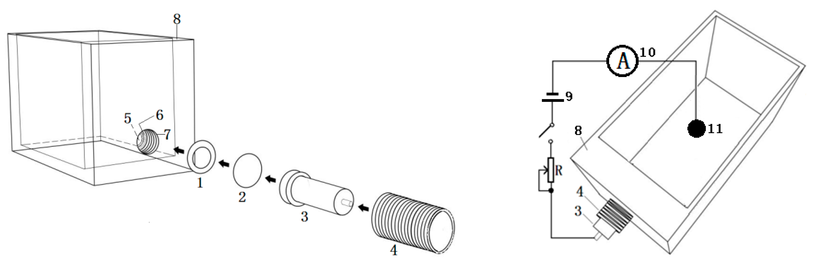
  • Ring-shaped adhesive pad;
  • Circular aluminium foil;
  • Reducer copper electrode;
  • Inner fastening screw;
  • Small cylindrical hole;
  • Small cylindrical hole annular enclosure;
  • Large cylindrical hole;
  • Electrolyser tank wall (acrylic material);
  • Voltage source (0–40 V);
  • Ammeter (0–3 A);
  • Carbon sphere electrode.
A high-purity aluminium foil (99.999%) was cut into 2 cm diameter discs and annealed under vacuum in a furnace at 400 °C for 2 h. The annealed discs were electropolished for 5 min in a solution of perchloric acid and anhydrous ethanol (1:4 by volume), then thoroughly cleaned with acetone and deionised water before drying. The pretreated aluminium foil served as the working electrode, while a custom-made carbon sphere electrode served as the counter electrode. Anodisation was performed at 30 V in a 6 wt% phosphoric acid solution as the electrolyte. A series of AAO films were fabricated by varying the electrode spacing and oxidation time using a single-step anodisation method. To prepare AAO films for subsequent use as working electrodes, anodisation was carried out at 30 V with an electrode spacing of 15 cm and an oxidation time of 12 min.
Co@AAO composite films were fabricated using a single-step AC deposition method. The working electrode was paired with the carbon sphere counter electrode, and the electrolyte consisted of a mixture of 0.12 mol/L CoSO4·7H2O and 0.39 mol/L boric acid. An AC voltage of 25 V was applied for 20 s. To investigate the effect of electrode spacing, Co@AAO composite films were prepared with electrode distances of 2, 3, 4, and 5 cm.
The structural colour of the films was characterised using a digital camera (Canon EOS600D). The micro-area morphology and crystal structure of the films were analysed using a scanning electron microscope (SEM, Hitachi S-4800, HV 20 kV, Hitachi Ltd., Tokyo, Japan) and an X-ray diffractometer (XRD, Cu-Kα), respectively. Magnetic properties were measured using a physical property measurement system (PPMS-6, Quantum Design, CA, USA).

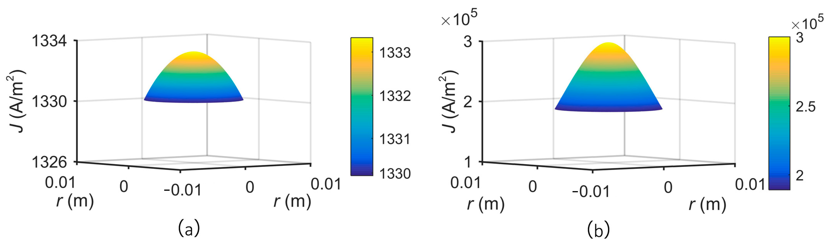
3. Theory and Simulation

The circular aluminium foil serves as the working electrode, with the carbon sphere acting as the counter electrode. The schematic diagram of the current line distribution during electrochemical anodisation is shown in Figure 2a. Based on electromagnetic field theory and high-field conduction theory, the surface current density of the AAO film is calculated as follows:
J = U 2 2 π R 0 h ( r 2 + h 2 ) 3 2
where r is the distance from any point on the surface of the circular aluminium foil to the centre, h is the distance from the carbon sphere to the aluminium foil, U2 is the voltage applied between the carbon sphere and the barrier layer (Al2O3), U1 is the voltage across the barrier layer, and R0 is the resistance of the electrolyte between the two electrodes.
According to Thompson’s findings [20], the current density on the AAO surface is expressed as
J = A e B U 1 d + J R J
where A e B U 1 d is the current density for the formation of aluminium oxide, d is the thickness of the barrier layer (Al2O3), and A and B are constants related to temperature and represent the current density for the dissolution of aluminium oxide. According to Kirchhoff’s current law, Equations (1) and (2) are equal:
J = U 2 2 π R 0 h ( r 2 + h 2 ) 3 2 = A e B U 1 d + J R J
Equation (3) establishes a connection between the electromagnetic field during anodisation and electrochemical theoretical predictions. When U2 and h remain constant, the total current density J in the electrolyte depends on r. The current density is equal at points on the film surface with the same r. At r = 0, J is at its maximum, leading to the fastest temperature increase and the thickest AAO film with the deepest pores and largest pore diameters. As r increases, J gradually decreases symmetrically outward, causing corresponding decreases in film thickness, pore depth, and pore diameter. When hr, the influence of r on current density becomes negligible, resulting in uniform current density across the film surface.
For electrochemical deposition, the schematic diagram of the current line distribution is shown in Figure 2b. The formula for the electrodeposition current density on the AAO film surface is calculated as
J p = U 2 2 π R 0 h ( r 2 + h 2 ) 3 2 = U U 1 2 π R 0 h ( r 2 + h 2 ) 3 2
where U is the voltage applied between the two electrodes, U2 is the voltage between the carbon spheres and the barrier layer (Al2O3), and U1 is the voltage across the barrier layer. According to Equation (4), when U, U1, and h remain constant, the deposition current density JP depends on r and is equal at points with the same r. At r = 0, JP is at its maximum, and as r increases, JP gradually decreases symmetrically outward.
Notably, a thick barrier layer leads to high resistance in Al2O3, causing the voltage U1 across the barrier layer to be approximately equal to U, resulting in JP approaching zero, thereby preventing electrodeposition. However, when the barrier layer is thin, Al2O3 exhibits diode-like unidirectional conductivity, enabling AC deposition.
Using MATLAB, the current density distribution was simulated, as shown in Figure 2a. For an oxidation voltage of 30 V and a distance of 15 cm between the carbon spheres and the aluminium foil, the plot of J as a function of the aluminium foil radius r is shown in Figure 3a. At r = 0, the maximum current density is 1333 A/m2. As r increases, J gradually decreases radially, reaching 1330 A/m2 at the film edge (r = 0.6 cm), with a gradient change rate (∆J/r) of 500 A/m3. In contrast, for the same oxidation voltage at a distance of 1 cm, J at r = 0 is 2.9 × 10⁵ A/m2 and decreases to 1.8 × 10⁵ A/m2 at the edge, resulting in a gradient change rate of 1.83 × 10⁷ A/m3, as shown in Figure 3b.

4. Results and Discussion

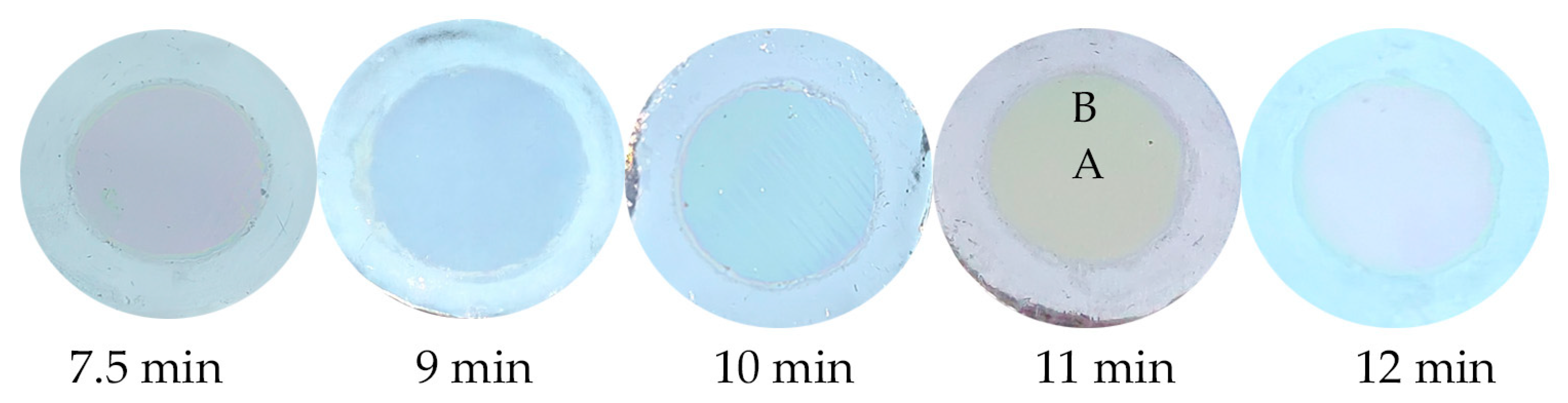
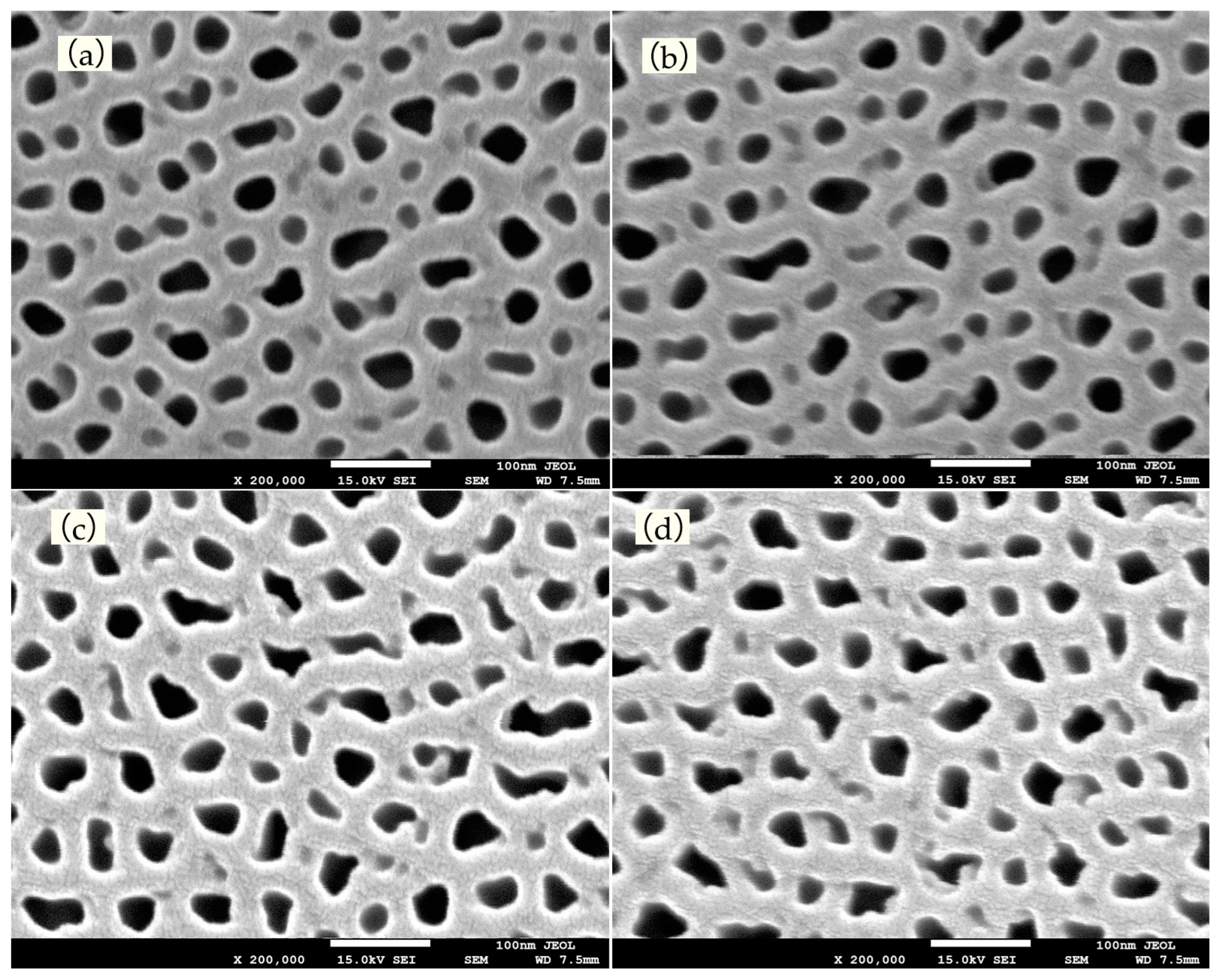
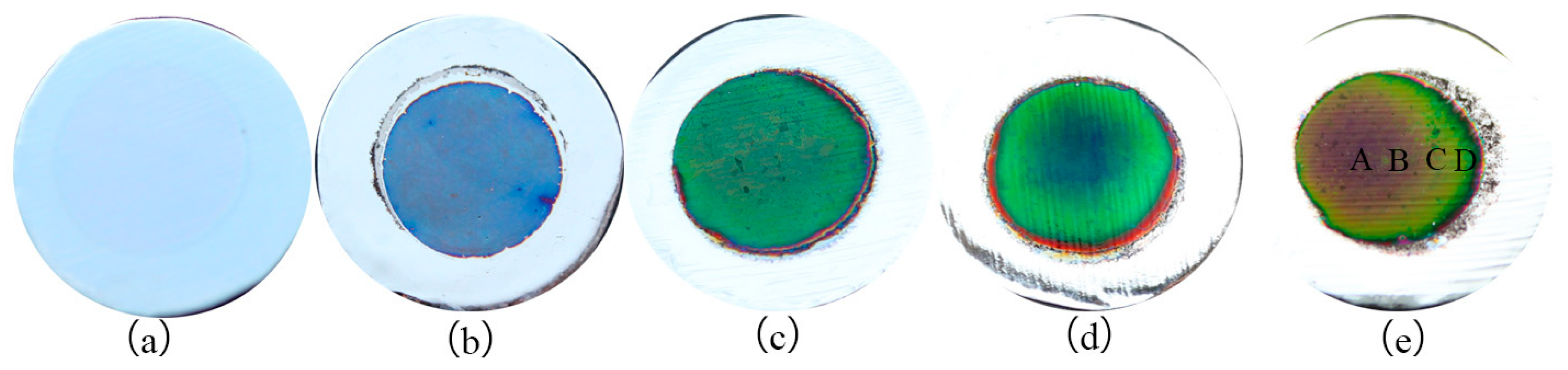
4.1. Experimental Results and Discussion of Anodic Oxidation

At an applied voltage of 30 V with an electrode distance (h) of 15 cm and an aluminium foil radius (r) of 0.6 cm (hr), digital photographs of AAO films prepared with oxidation times of 7.5, 9, 10, 11, and 12 min are shown in Figure 4.
From the figure, it is evident that the films exhibit a single structural colour, shifting with increasing oxidation time from purple to blue, green, yellow, and finally red. This structural colouration arises from the interference between light waves reflected from the upper (air–AAO interface) and lower (AAO–substrate interface) surfaces of the AAO films. The presence of a single structural colour suggests that the film thickness is approximately uniform, with minimal differences between central (region A) and edge (region B) areas. To confirm this, SEM analysis was conducted to examine the surface and cross-sections of different regions of an AAO film prepared at an oxidation voltage of 30 V and an oxidation time of 11 min, with SEM results shown in Figure 5.
Figure 5a,b show SEM surface images of regions A and B, respectively, and Figure 5c,d display SEM cross-section images of the same respective regions. Parameters such as pore diameter and pore depth of the AAO films were calculated from the SEM images and are summarised in Table 1. The data reveal that the pore diameter in region A is slightly larger, while region B contains more nascent pores, with the surface morphology resembling a Y-shaped structure. However, the differences in film thickness, porosity, refractive index, and other parameters between the two regions are insignificant.
The structural colour can be explained using the film interference equation [17]:
2 n d cos θ = ( 2 j + 1 ) λ 2
where n is the refractive index of the AAO film, d is the film thickness, θ is the angle of refraction, j is the order of interference, and λ is the wavelength of the interfering light. Considering the half-wave loss and assuming normal light incidence (θ = 0) with an interference order of j = 1, the calculated interference wavelengths of reflected light for regions A and B are 607 nm and 582 nm, respectively. These wavelengths fall within the yellow range of visible light, aligning with the structural colours shown in the digital photographs.
Using Equation (5), the interference wavelengths of reflected light for the central and edge regions of the AAO films shown in Figure 4 were calculated and are summarised in Table 2. In this analysis, region A corresponds to the central region of the film, while region B represents the edge region. Table 2 indicates that the film thickness in region A is slightly greater than in region B, with the thickness gradually decreasing symmetrically outward from the centre, forming a “bowl-shaped” profile. We calculated the specific surface area of a series of AAO films, as shown in Table 2, and found that it decreased with increasing oxidation time. This result reflects the fact that the total mass of the film and the pore length both increase during oxidation. However, according to the definition of specific surface area, the increase in mass due to pore length growth outweighs the increase in surface area, resulting in a reduction in specific surface area.
Due to the small thickness difference between regions A and B within the same film, the reflected light interference wavelengths fall within the same colour range, resulting in the appearance of a single, uniform colour. This observation is consistent with the theoretical calculations and MATLAB simulation results.
By combining experimental data with theoretical calculations, we examined the carbon sphere electrode anodisation process. When the electrode spacing is large (hr), the micro-area oxidation current distribution in AAO films symmetrically decreases from the centre outward. However, the minimal current density gradient leads to an approximately uniform current distribution across the film.
AAO films were also prepared with the distance between the carbon sphere electrode and the aluminium foil set to 1 cm through a single anodisation process at 30 V with oxidation times of 1, 2, 3, and 4 min, with digital photographs of these films revealing vibrant iridescent structural colours (Figure 6). With increasing oxidation time, the yellow structural colour ring at the centre of the film expands outward, while the centre sequentially transitions through red and green hues. Eventually, the yellow ring reaches the outermost edge, where the rings become denser, forming a distinct iridescent ring-like pattern.
The surface and cross-sectional characteristics of different regions of the AAO film anodised for 3 min were analysed using SEM. Figure 7a–d display the surface images of regions A–D, while Figure 8a–d show the corresponding cross-sectional images. The SEM results indicate that the pore size gradually decreases, the pore spacing gradually increases, and the thickness gradually decreases when moving outward from the centre of the film. In the central region, the pores are vertically aligned and fully penetrate the film, whereas in the edge regions, many pores are not fully penetrated and exhibit a Y-shaped structure.
The thickness, pore diameter, and other parameters of the AAO film, as obtained from SEM images and calculations, are listed in Table 3. The data indicate that the film’s thickness, pore radius, porosity, and refractive index gradually decrease from the centre outward. Within the visible light spectrum, the calculated interference wavelengths of reflected light for different regions align with the experimentally observed colours, confirming the validity of our theoretical analysis of carbon sphere electrode anodisation currents.
When natural light interacts with an AAO film where thickness, average pore radius, and pore depth decrease radially outward, the reflected light beams from the upper and lower surfaces of the film undergo equal-thickness interference, producing concentric iridescent rings. As the oxidation time increases, the number of colour rings grows, causing the ring pattern to become more compact. This occurs because longer oxidation times result in a uniform thickness increase across the film, but the rate of thickness growth is the highest at the centre and decreases outward due to the higher current density at the centre, driving more rapid growth in that region. Moving outward, the lower current density leads to progressively slower thickness growth, creating a larger thickness gradient along the radius as oxidation time increases. When the changes in film thickness exceed the wavelength range of a specific colour, the interference rings associated with that colour shift outward, and the overall ring pattern becomes increasingly compact.

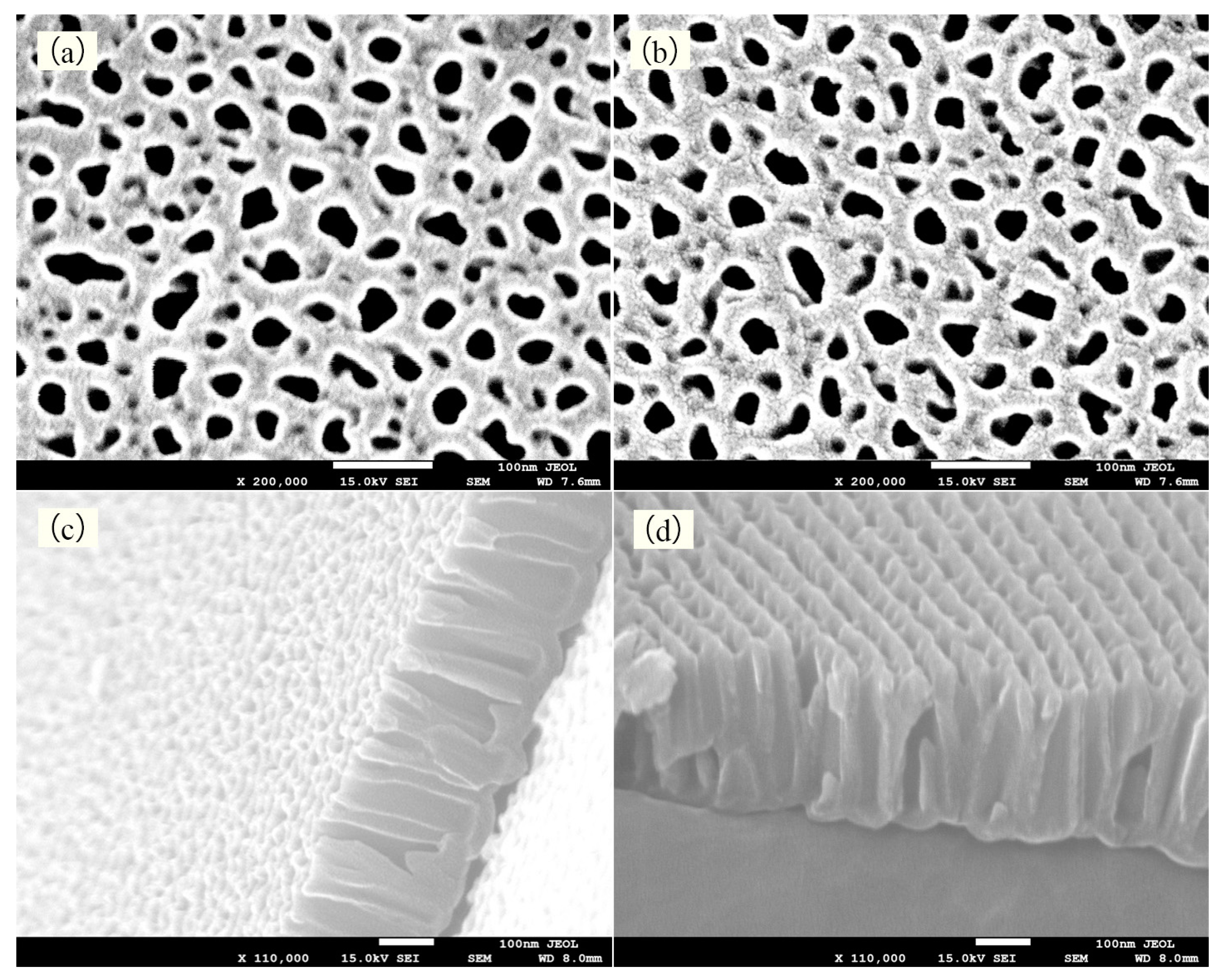
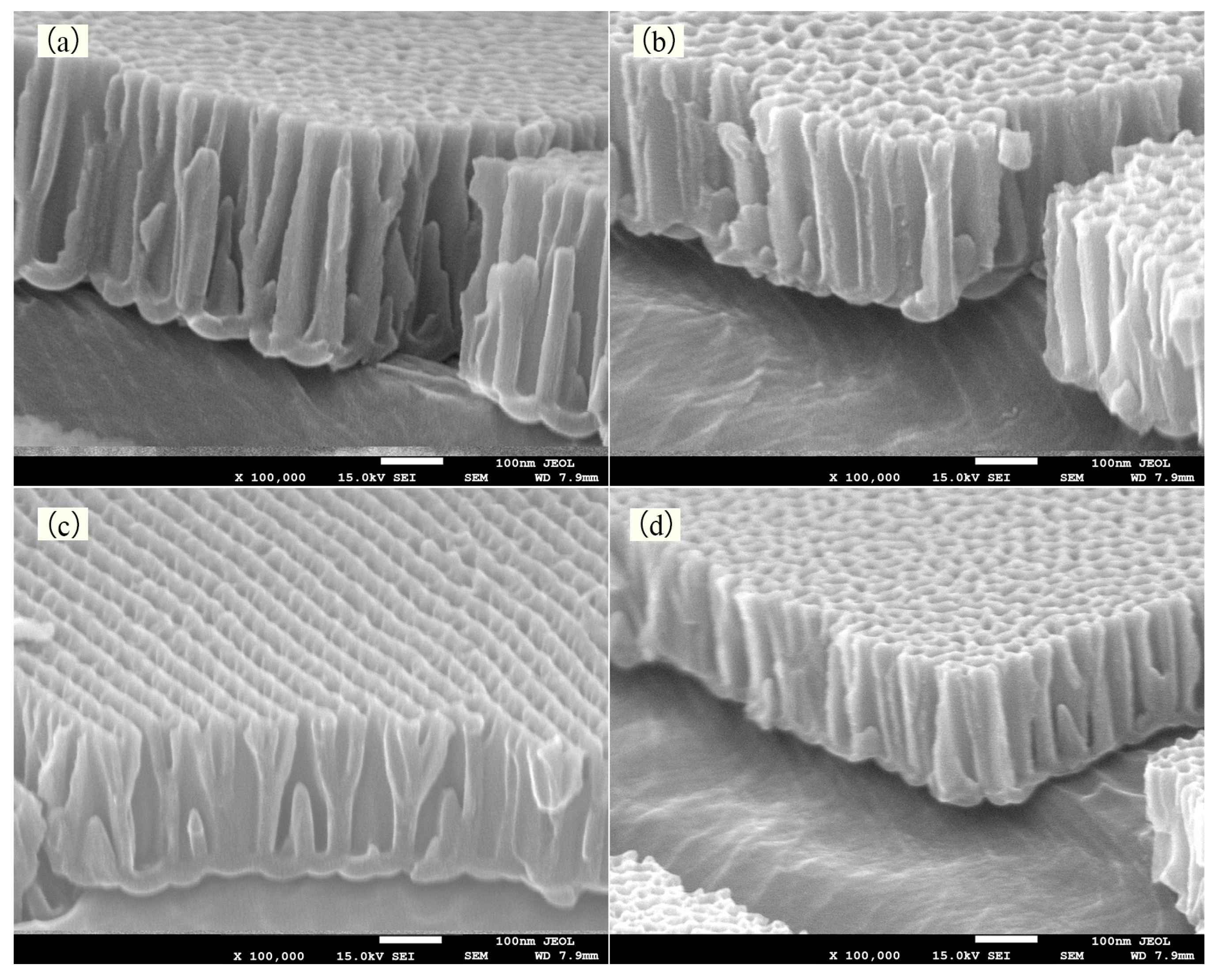
4.2. Experimental Results and Discussion of Electrodeposition

AAO films used as working electrodes were prepared by anodisation at an oxidation voltage of 30 V, with an electrode distance of 15 cm and an oxidation time of 12 min. A carbon sphere electrode served as the counter electrode, with distances between electrodes set to 2, 3, 4, and 5 cm. The electrolyte consisted of 0.12 mol/L CoSO4·7H2O and 0.39 mol/L boric acid. An AC voltage of 25 V was applied, and Co was deposited within the AAO nanopores via AC electrodeposition for 20 s, resulting in the creation of a series of Co@AAO composite films. Digital photographs of these films are shown in Figure 9, revealing that the AAO films exhibit an unsaturated light red colour prior to electrodeposition. After AC electrodeposition of Co, the colour saturation of the films increases because the Co nanowires effectively shield the AAO-Al layer from reflected light [13]. As the electrode distance decreases, the colour of the Co@AAO films transitions from a uniform blue to green, with the centre region appearing yellow. When the electrode distance is reduced further to 2 cm, the films display concentric rings of colour ranging from red to orange–yellow and green, radiating outward from the centre.
To further investigate the relationship between the microstructure and structural colour of the Co@AAO composite films, Figure 10 shows SEM cross-sectional images taken from different viewpoints of the film’s centre and edge, as shown in Figure 9e. Images (a–d) correspond to regions A–D, moving outward from the centre along the radius, as labelled in Figure 9e. The thickness, refractive index, interference wavelengths, and other parameters of the composite films, obtained from SEM images and calculations, are summarised in Table 4.
From Figure 10 it is evident that Co nanowires have grown at the bottom of the AAO nanopores, with their length gradually decreasing from the centre of the film outward. The composite film consists of two distinct layers: the upper air-Al2O3 layer (referred to as the M layer) and the lower Co-Al2O3 layer (referred to as the N layer). When light is incident perpendicularly, the film interference equation [17] is given by
2 n M d M + 2 n N d N = ( m + 1 2 ) λ
where dM and dN are the thicknesses of the M and N layers, respectively, nM and nN are their respective refractive indices, m is the interference order, and λ is the wavelength of the interference light. Calculations indicate that the interference wavelengths of different regions of the composite film correspond to colours consistent with experimental observations.
According to the theoretical sphere electrode deposition formula (4), the deposition current density is influenced by the electrode distance h. As h increases, the gradient of the deposition current density across the film decreases, resulting in minimal differences in the lengths of nanowires within the nanopores across different regions of the AAO film. This leads to a uniform microstructure and a single structural colour. Conversely, when h decreases, the deposition current density and its radial gradient across the AAO film increase, causing the length of the Co nanowires within the nanopores to rapidly decrease from the centre outward. Since the refractive index of Co nanowires is higher than that of air, the average refractive index of the film decreases from the centre outward, thereby increasing the optical path difference gradient. When this gradient exceeds the wavelength range of a specific colour, the composite film exhibits an iridescent ring-like structural colour pattern. A greater optical path difference gradient results in denser colour rings, closely aligning with predictions from Formula (4).
To investigate the magnetic properties of the Co@AAO composite films, M-H curves were plotted at room temperature for regions A and C of the composite film shown in Figure 9e, with the magnetic field aligned parallel to the nanowire direction. The results, presented in Figure 11, demonstrate clear ferromagnetic behaviour, with saturation magnetisation values of 110 emu/cm3 and 87 emu/cm3 for regions A and C, respectively.
Compared to measurements with the magnetic field perpendicular to the nanowire direction, these results indicate that the easy magnetisation direction of the Co nanowires aligns with their long axis, suggesting that the magnetic properties of the Co@AAO composite films are primarily governed by shape anisotropy rather than magnetocrystalline anisotropy. Additionally, the observed decrease in saturation magnetisation from the centre outward indirectly confirms that the Co nanowires are longer in the central region of the film, resulting in a higher Co content within the AAO nanopores per unit area in this region.

5. Conclusions

This study provides both theoretical and experimental insights into the anodisation of metallic aluminium and the electrodeposition process using a carbon sphere electrode as the counter electrode and AAO as the working electrode. The results demonstrate that under constant experimental conditions, the anodisation and deposition current densities are governed by the distance between the electrodes and the radius of the working electrode, with the current density distribution gradually radially decreasing from the centre of the film outward.
When the electrode distance is much greater than the radius of the working electrode, the oxidation or deposition current density gradient is relatively small, leading to a uniform film microstructure with consistent optical and magnetic properties. In contrast, when the electrode distance is comparable to the size of the working electrode, the current density gradient becomes more pronounced, resulting in greater radial variations in the film microstructure and distinct optical and magnetic characteristics.
The experimental findings closely align with theoretical calculations and MATLAB simulations, supporting the validity of the proposed results. The use of a carbon sphere counter electrode for anodisation or electrodeposition can effectively tune the optical and magnetic properties of AAO, underscoring the significant potential of AAO and its composites for applications in fields related to anti-counterfeiting, drug delivery, catalysis, and sensors.

Author Contributions

Conceptualisation, J.G. and S.Y.; methodology, Y.Q.; software, A.W. and J.G.; validation, A.W.; formal analysis, S.Y. and W.H.; investigation, J.G. and Y.Q.; resources, X.L. and G.S.; data curation, X.L.; writing—original draft preparation, S.Y. and J.G.; writing—review and editing, S.Y.; visualisation, J.G.; supervision, G.S. and W.H.; project administration, J.G. and Y.Q.; funding acquisition, S.Y. and J.G. All authors have read and agreed to the published version of the manuscript.

Funding

This research was funded by the Chengde City Basic Research Project [Grant No. 202205B078], the Chengde City Science and Technology Plan Project [Grant No. 202304B019, 202205B090], and the Chengde City Science and Technology Innovation Project [Grant No. HZLC2024019, HZLC2024006].

Data Availability Statement

Data sharing does not apply to this article.

Conflicts of Interest

The authors declare no conflicts of interest.

References

  1. Kushnir, S.E.; Napolskii, K.S. Thickness-dependent iridescence of one-dimensional photonic crystals based on anodic alumina. Mater. Des. 2018, 144, 140–150. [Google Scholar] [CrossRef]
  2. Liu, S.X.; Tian, J.L.; Zhang, W. Fabrication and application of nanoporous anodic aluminum oxide: A review. Nanotechnology 2021, 32, 222001. [Google Scholar] [CrossRef] [PubMed]
  3. Tabrizi, M.A.; Ferré-Borrull, J.; Marsal, L.F. An optical biosensor for the determination of cathepsin B as a cancer-associated enzyme using nanoporous anodic alumina modified with human serum albumin-thionine. Microchim. Acta 2020, 187, 230. [Google Scholar] [CrossRef] [PubMed]
  4. Lu, P.H.D.; Lin, D.; Wang, X.; Lennon, A. Laser doping through anodic aluminium oxide silicon solar cell. Sol. Energy Mater. Sol. Cells 2016, 145, 349–357. [Google Scholar] [CrossRef]
  5. Acosta, L.K.; Law, C.S.; Santos, A.; Ferré-Borrull, J.; Marsal, L.F. Tuning intrinsic photoluminescence from light-emitting multispectral nanoporous anodic alumina photonic crystals. Marsal 2022, 7, 026108. [Google Scholar] [CrossRef]
  6. Sachiko, O.; Hidetaka, A. A new perspective on pore growth in anodic alumina films. Electrochem. Commun. 2021, 124, 106972. [Google Scholar]
  7. Pappas, J.M.; Thakur, A.R.; Dong, X. Effects of zirconia doping on additively manufactured alumina ceramics by laser direct deposition. Mater. Des. 2020, 192, 108711. [Google Scholar] [CrossRef]
  8. Szwachta, G.; Januszewska, B.; Włodarski, M.; Norek, M. From gradient-index to step-index filters: A switch between the two types of photonic crystals induced by the amplitude and period of sinusoidal function applied during high-temperature anodisation of aluminium. Appl. Surf. Sci. 2023, 607, 155031. [Google Scholar] [CrossRef]
  9. Domínguez-Adame, F.; Martín-González, M.; Sánchez, D.; Cantarero, A. Nanowires: A route to efficient thermoelectric devices. Phys. E 2019, 113, 213–225. [Google Scholar] [CrossRef]
  10. Manzano, C.V.; Martin-Gonzalez, M. Electrodeposition of V-VI Nanowiresand Their Thermoelectric Properties. Front. Chem. 2019, 7, 516. [Google Scholar] [CrossRef] [PubMed]
  11. Ruiz-Clavijo, A.; Caballero-Calero, O.; Martín-González, M. Revisiting anodic alumina templates: From fabrication to applications. Nanoscale 2021, 13, 2227–2265. [Google Scholar] [CrossRef] [PubMed]
  12. Evertsson, J.; Vinogradov, N.A.; Harlow, G.S. Self-organization of porous anodic alumina films studied in situ by grazing-incidence transmission small-angle X-ray scattering. RSC Adv. 2018, 8, 18980–18991. [Google Scholar] [CrossRef] [PubMed]
  13. Kima, B.; Youn, Y.; Park, Y.-S. Impurity-driven formation of branched pores in porous anodic alumina. Scr. Mater. 2016, 122, 102–105. [Google Scholar] [CrossRef]
  14. Roslyakova, I.V.; Gordeeva, E.O.; Napolskii, K.S. Role of Electrode Reaction Kinetics in Self-Ordering of Porous Anodic Alumina. Electrochim. Acta 2017, 241, 362–369. [Google Scholar] [CrossRef]
  15. Białek, E.; Włodarski, M.; Norek, M. Influence of Anodization Temperature on Geometrical and Optical Properties of Porous Anodic Alumina(PAA)-Based Photonic Structures. Materials 2020, 13, 3185–3194. [Google Scholar] [CrossRef] [PubMed]
  16. Kant, K.; Low, S.P.; Marshal, A.; Shapter, J.G.; Losic, D. Nanopore gradients on porous aluminum oxide generated by nonuniform anodization of aluminum. Appl. Mater. 2010, 2, 3447–3454. [Google Scholar] [CrossRef] [PubMed]
  17. Yang, S.M.; Han, W.; Gu, J.J.; Li, H.T.; Qi, Y.K. Preparation and study of anodic alumina thin films with rainbow rings. Acta Phys. Sin. 2015, 64, 076102. (In Chinese) [Google Scholar] [CrossRef]
  18. Qi, Y.K.; Yang, S.M.; Li, X.; Wang, H.M.; Xu, Q.; Gu, J.J. Design of alumina composite films with gradual structural color and magnetism using non-uniform electric field. Thin Solid Film. 2021, 740, 138999. [Google Scholar] [CrossRef]
  19. Qi, Y.K.; Gu, J.J.; Shi, G.C.; Li, X.; Wang, A.; Yang, S.M. Symmetrically Controlled Design of Twin Alumina-Co Composite Thin Films. Coatings 2022, 12, 223. [Google Scholar] [CrossRef]
  20. Thompson, G.E.; Wood, G.C. Treatise on Materials and Technology; Academic Press: New York, NY, USA, 1983; Volume 23, pp. 269–271. [Google Scholar]
Figure 1. Schematic diagram of electrochemical reaction electrolyser.
Crystals 14 01102 g001
Figure 2. Schematic diagrams of the current lines for a carbon sphere electrode: (a) anodic oxidation; (b) electrodeposition.
Crystals 14 01102 g002
Figure 3. Current density diagram of MATLAB simulation with different electrode spacing: (a) h = 15 cm; (b) h = 1 cm.
Crystals 14 01102 g003
Figure 4. Digital photos of AAO thin films oxidised with a voltage of 30 V, electrode spacing of 15 cm for 7.5, 9, 10, 11, and 12 min. The regions labeled A and B correspond to the center and edge regions of the film, respectively.
Crystals 14 01102 g004
Figure 5. SEM images of the surface and cross-section of the AAO thin film with an oxidation voltage of 30 V and an electrode distance of 15 cm for 11 min. (a) surface image of region A; (b) surface image of region B; (c) cross-section image of region A; (d) cross-section image of region B.
Crystals 14 01102 g005
Figure 6. Digital photos of AAO thin films oxidised with a voltage of 30 V, electrode spacing of 1 cm for 1, 2, 3, and 4 min. The regions labeled A, B, C, and D correspond to distinct color zones extending outward from the film center.
Crystals 14 01102 g006
Figure 7. SEM images of the surface of the AAO thin film. Parts (ad) correspond to positions A to D in Figure 6 (3 min).
Crystals 14 01102 g007
Figure 8. SEM images of the cross-section of the AAO thin film. Parts (ad) correspond to positions A to D in Figure 6 (3 min).
Crystals 14 01102 g008
Figure 9. Digital photos of AAO and Co@AAO composite films: (a) AAO thin films oxidised with a voltage of 30 V, electrode spacing of 15 cm for 12 min; (be) corresponding Co@AAO composite films were deposited with a voltage of 25 V for 20 s with electrode spacing of 5, 4, 3, and 2 cm, respectively.
Crystals 14 01102 g009
Figure 10. SEM images of the cross-section of the Co@AAO composite film. Parts (ad) correspond to positions A to D in Figure 9e.
Crystals 14 01102 g010
Figure 11. Hysteresis loops of the Co@AAO composite film at room temperature. Curves A and C correspond to positions A and C in Figure 9e.
Crystals 14 01102 g011
Table 1. The data of AAO thin films oxidised with a voltage of 30 V, electrode spacing of 15 cm, and time of 11 min.
PositionAB
Aperture radius/(nm)109
Aperture pitch/(nm)5346
Porosity (%)1314
Refractive index1.571.56
Interference levels11
Thickness/(nm)290280
Wavelengths/(nm)607582
Corresponding colourYellowYellow
Table 2. The data of AAO thin films oxidised with a voltage of 30 V, electrode spacing of 15 cm, and time from 7.5 to 12 min.
Time/(min)7.59101112
PositionABABABABAB
Thickness/(nm)198191238230264255290280317306
Wavelengths/(nm)414397498478553530607582664636
Specific surface area (m2/g)9.158.748.558.398.25
Corresponding colourPurplePurpleBlueBlueGreenGreenYellow Yellow RedRed
Table 3. The data of AAO thin films oxidised with a voltage of 30 V, electrode spacing of 1 cm, and time of 3 min.
PositionABCD
Aperture radius/(nm)20181614
Aperture pitch/(nm)56606877
Porosity0.460.330.200.12
Refractive index1.411.431.521.57
Interference levels1111
Thickness/(nm)387283250215
Wavelengths/(nm)728540507440
Corresponding colourRedYellowGreenBlue
Table 4. The data of Co@AAO thin films electrodeposited with AC voltage of 25 V, electrode spacing of 2 cm, and time of 20 s.
Refractive IndexM Layer: n air-Al2O3 = 1.57N Layer: n Co-Al2O3 = 1.67
PositionABCD
Thickness/(nm)313300269269
Thickness of air-Al2O3/(nm)119150165194
Thickness of Co-Al2O3/(nm) 19415010475
Interference levels1111
Wavelengths/(nm)681648599573
Corresponding colourRedRedOrange–yellowGreen
Disclaimer/Publisher’s Note: The statements, opinions and data contained in all publications are solely those of the individual author(s) and contributor(s) and not of MDPI and/or the editor(s). MDPI and/or the editor(s) disclaim responsibility for any injury to people or property resulting from any ideas, methods, instructions or products referred to in the content.

