Article

Determination of Thermal Damage Threshold in THz Photomixers Using Raman Spectroscopy

1
Ernst-Ruska-Centre (ER-C-2), Forschungszentrum Jülich, 52425 Jülich, Germany
2
Jülich-Aachen Research Alliance (JARA), Fundamentals of Future Information Technology, 52425 Jülich, Germany
3
Peter Grünberg Institute (PGI-6), Forschungszentrum Jülich, 52425 Jülich, Germany
4
Materials Science Program and Laboratory for Laser Energetics, University of Rochester, Rochester, NY 14627, USA
5
Department of Electrical and Computer Engineering and Laboratory for Laser Energetics, University of Rochester, Rochester, NY 14627, USA
6
Rochester Institute of Technology, Rochester, NY 14623, USA
*
Authors to whom correspondence should be addressed.
Crystals 2023, 13(8), 1267; https://doi.org/10.3390/cryst13081267
Submission received: 27 July 2023 / Revised: 11 August 2023 / Accepted: 16 August 2023 / Published: 17 August 2023
(This article belongs to the Special Issue Raman Spectroscopy of Crystalline Materials and Nanostructures)

Abstract

:
The increase of device lifetime and reliability of THz photomixers will play an essential role in their possible future application. Therefore, their optimal work conditions/operation range, i.e., the maximal incident optical power should be experimentally estimated. We fabricated and tested THz photomixer devices based on nitrogen-implanted GaAs integrated with a Bragg reflector. Raman spectroscopy was applied to investigate the material properties and to disclose any reversible or irreversible material changes. The results indicate that degradation effects in the photomixer structures/material could be avoided if the total optical power density does not exceed levels of about 0.7 mW/µm2 for 100 min of operation. Furthermore, the investigations performed during 1000 min of optical exposure on the photomixer devices’ central region comprising interdigitated metal-semiconductor-metal (MSM) structures suggest a reversible “curing” mechanism if the power density level of ~0.58 mW/µm2 is not exceeded. Long-term operation (up to 1000 h) reveals that the photomixer structures can withstand an average optical power density of up to ~0.4 mW/µm2 without degradation when biased at 10 V. Besides the decrease of the position of the A1g (LO) Raman mode from ~291 cm−1 down to ~288 cm−1 with increasing optical power density and operation time, broad Raman modes evolve at about 210 cm−1, which can be attributed to degradation effects in the active photomixer/MSM area. In addition, the performed carrier lifetime and photomixer experiments demonstrated that these structures generated continuous wave sub-THz radiation efficiently as long as their optimal work conditions/operation range were within the limits established by our Raman studies.

1. Introduction

Enormous progress was made on the development of THz continuous wave (cw) photomixers during the last ~3 decades, as can be seen from the chronology of events documented by selected publications [1,2,3,4,5,6,7,8,9,10,11,12,13,14,15,16,17,18,19,20,21,22,23,24,25,26,27,28,29,30,31,32,33,34,35,36,37,38,39,40,41,42,43,44,45,46,47,48,49]. This is related to the advancement of materials [1,2,7,11,14,16,17,22,44,45] such as low-temperature–grown GaAs (LT-GaAs) and others, e.g., implanted III-V materials introduced into their structures on the one hand, and on the development of photodetectors [6,13,15,20,23,28,29,42,44] and of photomixers [3,4,5,8,9,10,12,13,18,19,24,26,30,31,32,33,34,38,39,46,47,49] on the other hand. However, there still is a lack of highly efficient solutions. In the past, THz photomixers were utilized in a large range of applications, such as in THz spectroscopy techniques, radar, communication, or local oscillators in radio-astronomy. However, long-term device operation as well as output power stability and reliability seem to be limited predominantly by material degradation effects. Here, in this study, we focus our attention on the determination of the safe operating conditions and “work range” for the incident optical power applied in THz photomixer structures. Since Raman spectroscopy is very sensitive to structural changes, it is predestined to be the suitable technique for this task. To this end, we investigated the evolution of characteristic Raman modes in the implanted GaAs material. The experimental determination of the suitable operation range plays an important role, since the “maximal” THz output levels in our photomixer structures should be generated in long-term operation periods. Therefore, we tested optically our structures with total power levels ranging from 1 up to 50 mW at 780 nm wavelength. We identified the “critical” high optical power region in which there are indications of irreversible material/structural changes by recording position changes of the Raman shift in comparison with their non-exposed device counterparts. Subsequently, our THz photomixer structures were tested under the estimated “safe” operational conditions for up to 1000 h. We observed no indication for degradation effects, which confirms that a careful estimation of the optimal operation conditions could significantly increase the device “lifetime” and reliability. Subsequently, the N-implanted GaAs photomixers were used to generate sub-THz cw radiation, by mixing down two cw laser signals with wavelengths in the 760–800 nm range.

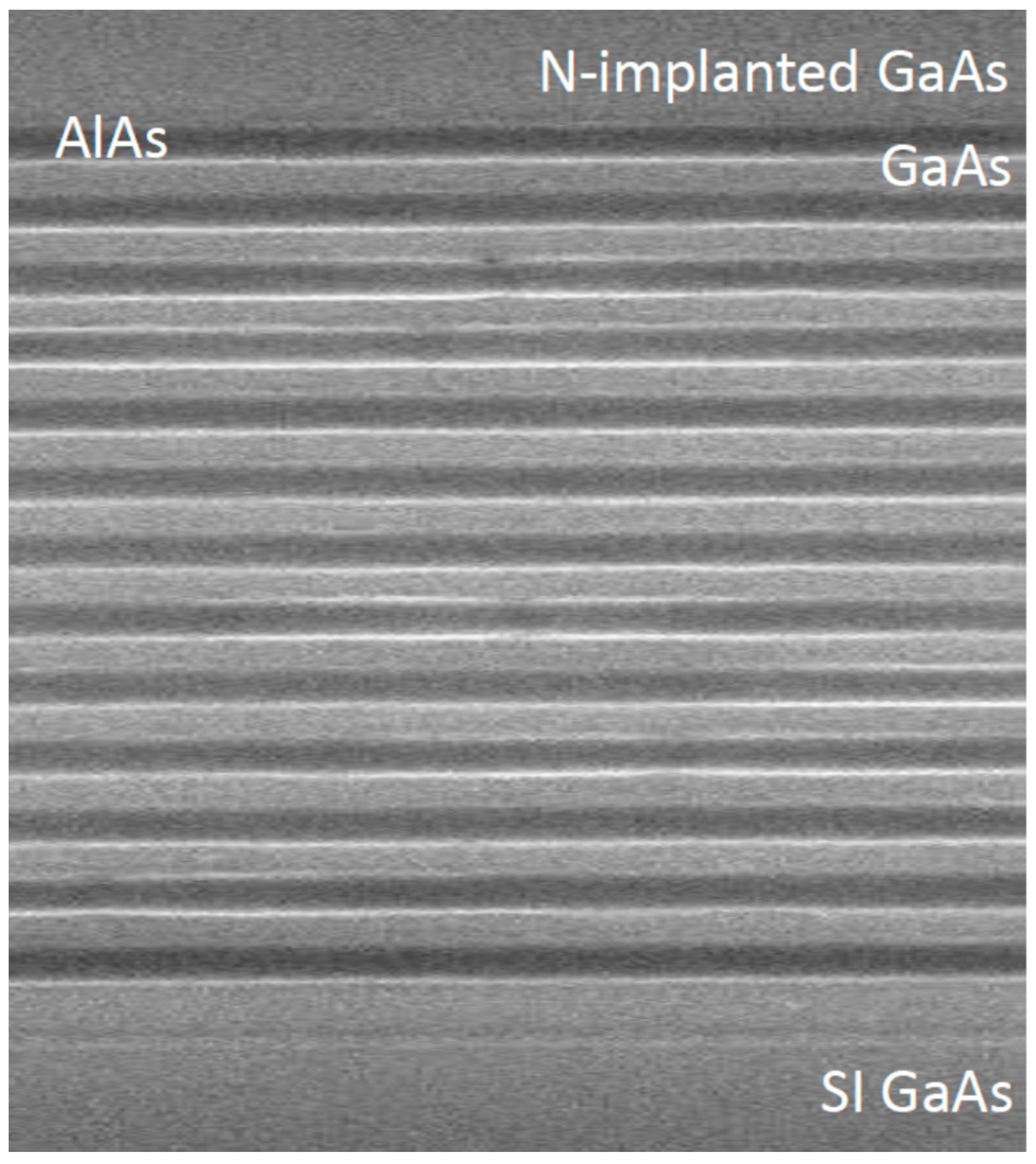
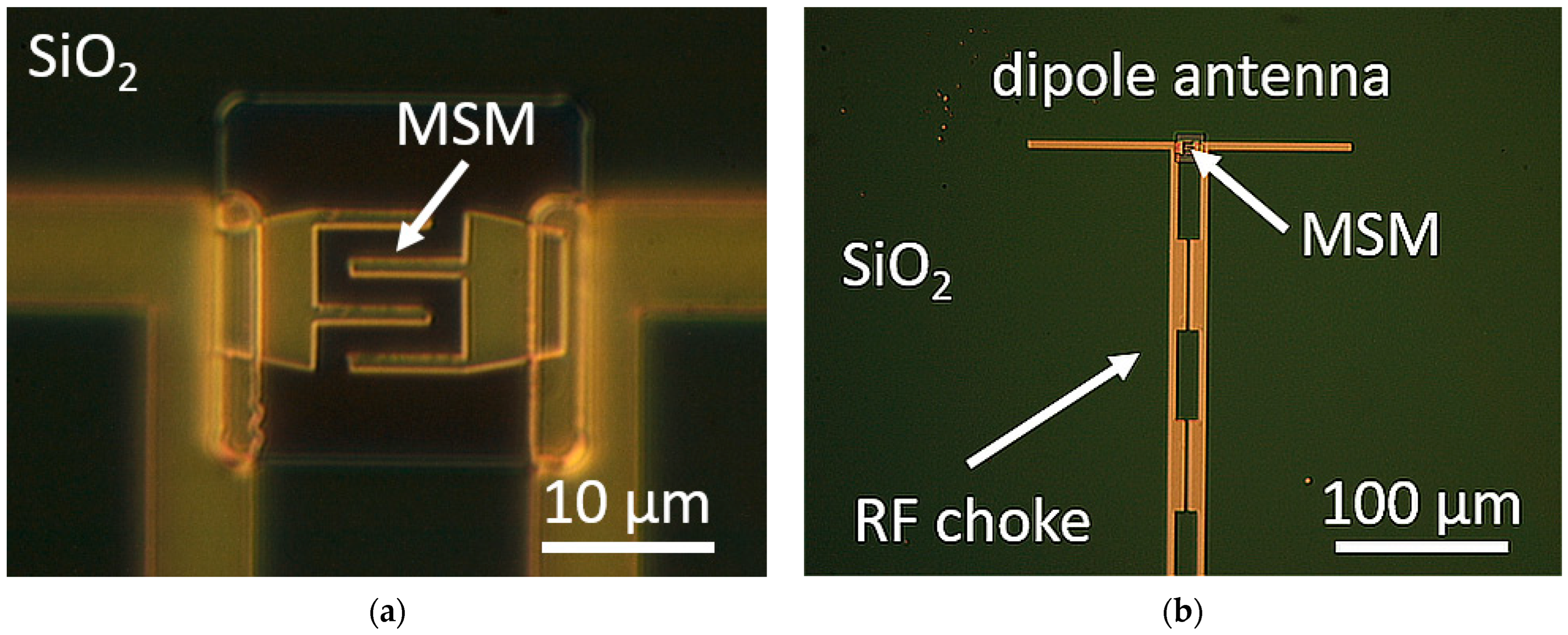
2. Materials and Methods

We started the fabrication process unconventionally for the research III-V material “family”, where molecular beam epitaxial (MBE) techniques are mostly applied, by using a metalorganic vapor phase epitaxy (MOVPE, AIXTRON, Herzogenrath, Germany) technique to deposit GaAs layers on 2-inch, (100) oriented, semi-insulating GaAs substrates. The MOVPE technique is—in contrast to MBE—a very versatile technique, which allows the deposition of many micrometer-thick epitaxial films, as well as layers down to the nanometer scale with precise composition control reproducibly and is, therefore, the preferred deposition method for the industry. By applying the so-called “nitrogen” process, in which nitrogen is used as the carrier and ambient gas instead of hydrogen, the efficiency has been greatly improved with respect to precursor exploitation and layer uniformity, creating a cost-effective process with, additionally, increased safety [50,51]. After depositing a 100 nm thick GaAs buffer layer, 12 periods of AlAs/GaAs (67 nm/55 nm) were grown serving as a Bragg mirror, succeeded by a 500 nm cap layer of GaAs. The growth temperature and reactor pressure were kept at 650 °C and 20 hPa, respectively. The layer thicknesses of the AlAs/GaAs layer system used for the Bragg mirror were chosen for a maximal reflectivity in the wavelength range between ~770 nm and ~800 nm. Figure 1 presents a scanning electron micrograph (SEM) cross-sectional view of the AlAs/GaAs layers. Very smooth and abrupt interfaces, as well as uniform layer thickness are observed.
In the following, samples were implanted with 191 keV nitrogen ions and an implantation dose of ~8.1011 ions/cm2. Subsequently, 3 samples were annealed in nitrogen-ambient for 10 min at 300 °C, 350 °C, and 400 °C [52]. After the annealing process, photomixer structures were fabricated using e-beam and conventional lithography [12]. The technological process started with the fabrication of interdigitated metal-semiconductor-metal (MSM) structures with a finger width of 200 nm and a finger spacing of 1.8 µm. The MSM contact metallization was realized by the evaporation of Ni/AuGe/Ni/Au layer stacks with a total thickness of 200 nm and, subsequent, annealing with the help of a LMA (laser micro annealing) procedure [53] to improve the Ohmic contacts. In the next step, the complete surface area except for the MSM region was covered in 2 steps with SiO2 layers. They serve as electrical isolation layers for further metallic structures. For the sake of suppressing a pinhole formation in the SiO2 layer, the following procedure was applied: in a first step, 100 nm of SiO2 was deposited and then the sample was rotated by 90° and the next 100 nm thick SiO2 layer was deposited. Again, a conventional lithographical process was used for the fabrication of the resonant dipole antenna and the RF choke, which were connected with the MSM structure for the THz wave generation via optical mixing. Optical micrograph images of an MSM structure and the one integrated with a resonant dipole antenna and RF choke are presented in Figure 2a,b, respectively.
After the THz photomixers were fabricated, they were exposed to total optical power levels ranging from 1 up to 50 mW at 780 nm wavelength with exposure times between 1 and 1000 min, and characterized using Raman spectroscopy. The Raman studies were carried out in a confocal Raman microscope (Renishaw, New Mills, Gloucestershire, UK) in backscattering geometry, which was equipped with a frequency-doubled Nd-YAG laser (532 nm, 50 mW) and a CCD detector. The spectrometer was referenced to the transverse optical phonon of Si at 521 cm−1. Spectra were recorded in the range between 100 cm−1 and 500 cm−1. The experiments were done in a step-by-step fashion. Explicitly, after the exposure procedure under the respective optical power level (780 nm laser), the sample was then characterized by Raman scattering measurements (532 nm laser).

3. Results

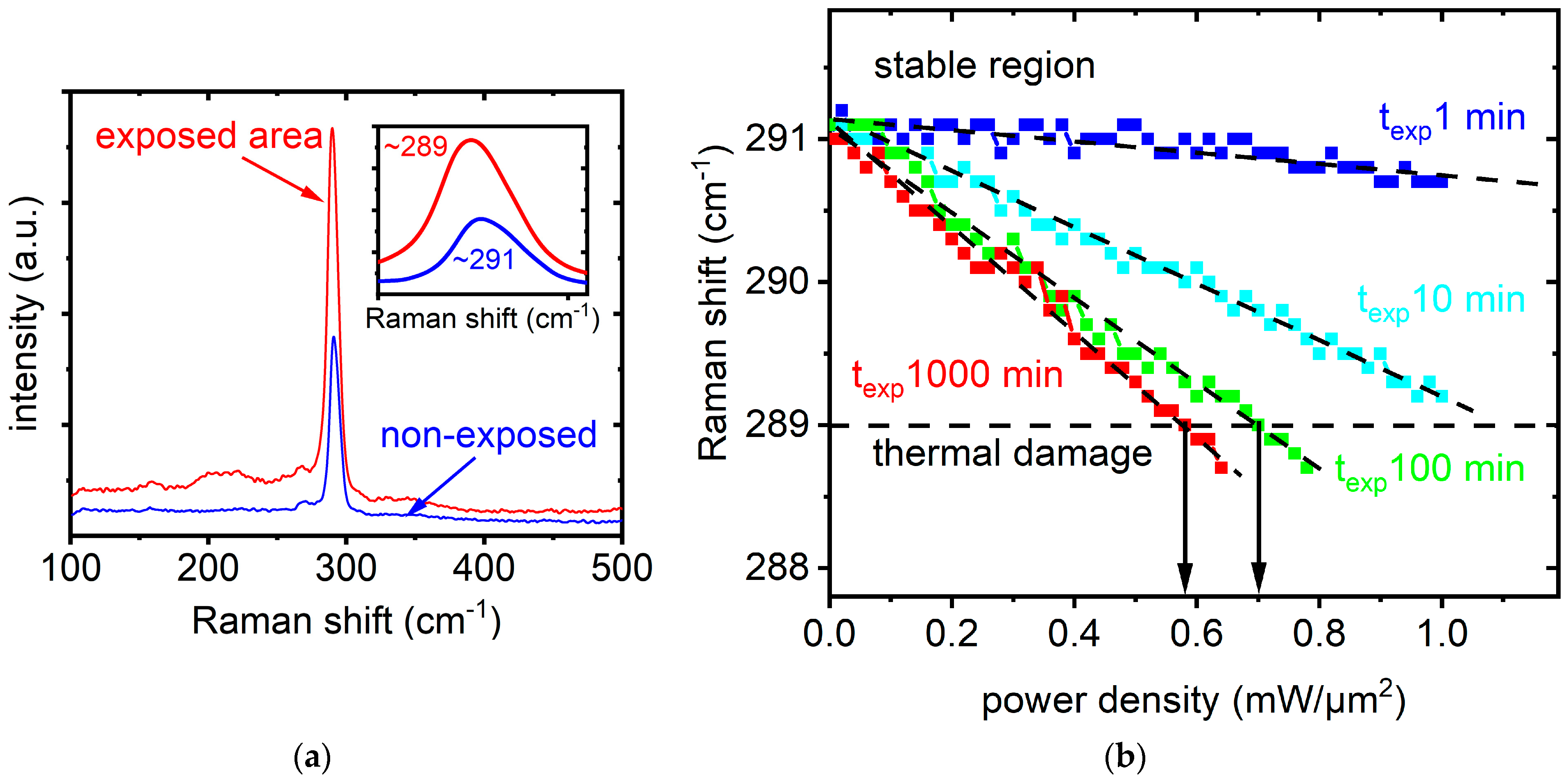
3.1. Raman Spectroscopy Investigations

The general effect of laser exposure (780 nm) on a THz photomixer structure is presented in Figure 3a. Both exemplary spectra, for the exposed (red) and non-exposed (blue) areas, of the structures are dominated by the A1g (LO) phonon mode of GaAs. Additionally, they both exhibit weaker modes at ~270 cm−1 and at ~165 cm−1. The higher Raman shift is attributed to the transverse optical (TO) phonon mode, symmetry forbidden according to the selection rules for (001) GaAs, due to crystalline disorder normal to the substrate surface [54,55,56] and to second order scattering, respectively. However, on closer inspection of these two spectra, differences become discernable: firstly, the position of the A1g (LO) mode shifts from 291 cm−1 to 289 cm−1 after exposure. In addition, two broad bands are observed at ~200 cm−1 and at ~210 cm−1 in the spectrum recorded at the exposed area. These Raman bands may be attributed to amorphous As and the disorder activated longitudinal acoustic mode (DALA)—indications of irreversible material degradation [55,56,57]. They emerge in the spectrum when the A1g (LO) mode shifts below 289 cm−1. Furthermore, the exposed area exhibits a higher intensity of the A1g (LO) mode than the non-exposed area. This intensity increase can be related to several factors, such as, e.g., reflectivity changes. In our study, the intensity increase is caused primarily by thermal effects. As soon as the thermal damage threshold is reached by the high incident optical power density, different defect types, possibly also oxides reported to be related to a high Raman intensity [58,59,60,61], develop.
Since the position of the Raman A1g (LO) mode of GaAs has been reported to be extremely sensitive to material properties such as crystallinity, thermal damage, and strain [55,62], it was employed to study the effect of incident optical power density for different exposure times (texp). The results are presented in Figure 3b. Each data point was achieved by recording a Raman spectrum after exposing the material for texp at the respective power density. The position of the A1g (LO) mode was then evaluated. As the power density increases, a continuous “red/down” shift of the A1g (LO) mode is found. The slope of this shift increases as the texp increases. In the following, it was confirmed by microscope inspection that degradation, i.e., melting occurs for structures, which exhibit a Raman shift below 289 cm−1. Here, obviously, the thermal damage threshold has been exceeded. The “critical” high optical power density region in which there are indications of irreversible material/structural changes can then, therefore, be determined. We found that the photomixer structures can withstand an average optical power density of up to ~0.7 mW/µm2 and ~0.58 mW/µm2 for texp of 100 and 1000 min, respectively, at room temperature when biased at 10V. Above these optical power densities, a combination of optical and Ohmic heating causes non-reversible structural changes, and the thermal damage threshold is exceeded.
Figure 4a,b show exemplary images obtained from micro-Raman intensity mappings collected in the central area of the interdigitated MSM structure without and with indication of degradation/thermal damage. A uniform intensity is observed for structures without any indication of damage, whereas strongly non-uniform intensity is observed for structures indicating degradation. In this region, thermal degradation in the photomixer MSM active region was additionally confirmed by microscope inspection.

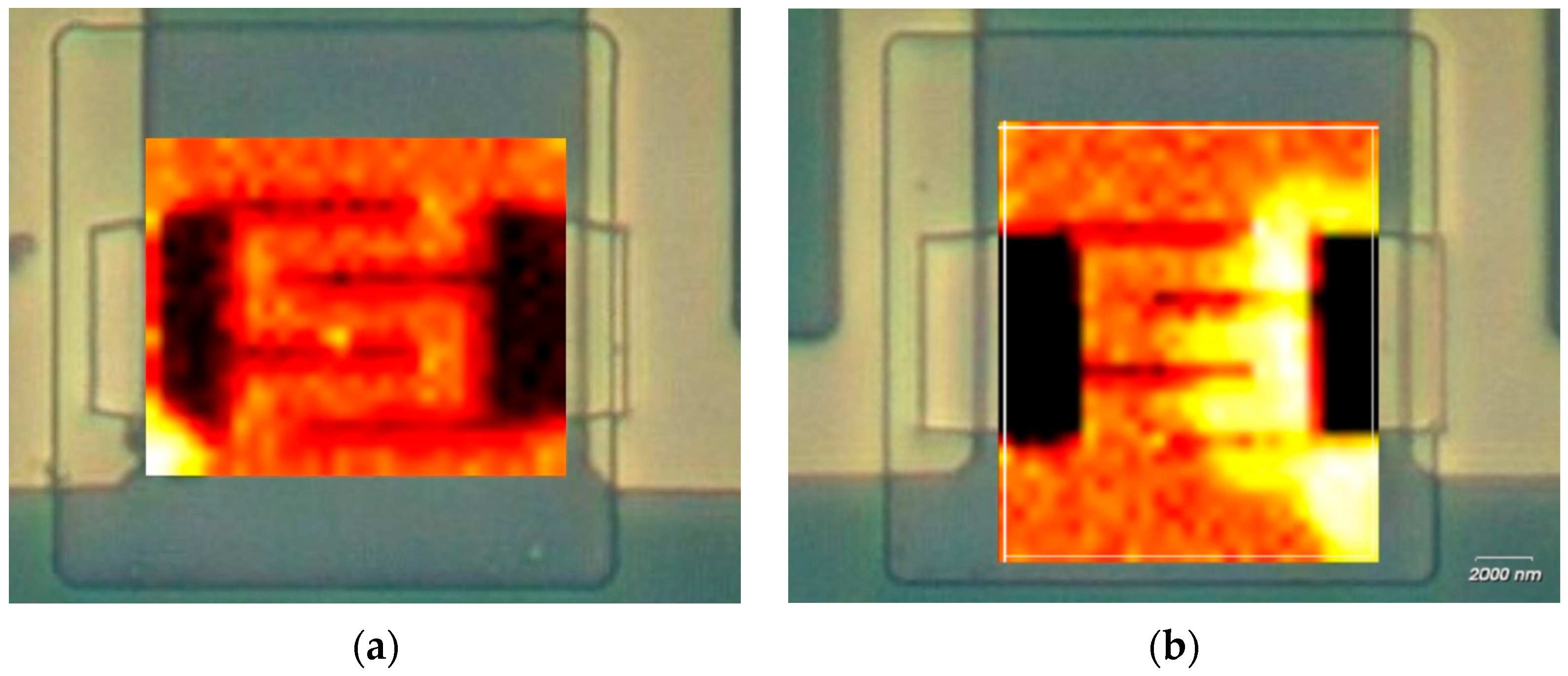
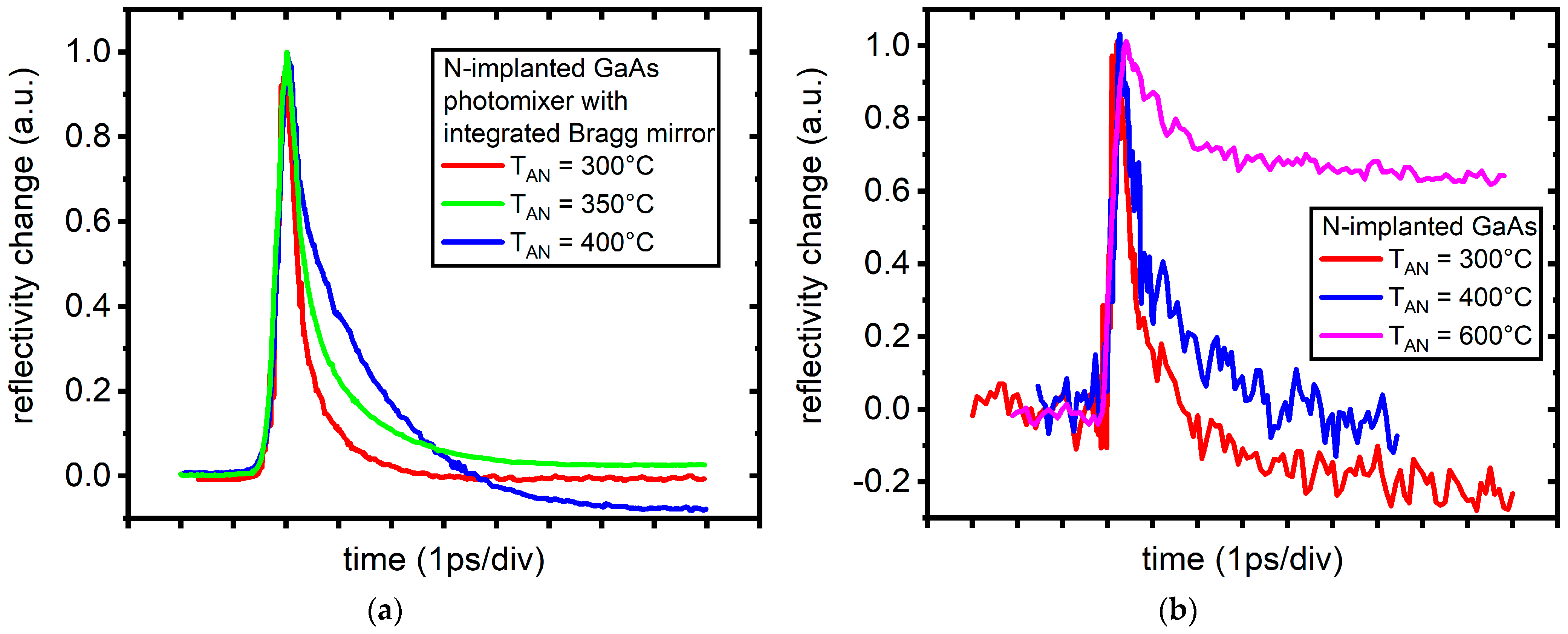
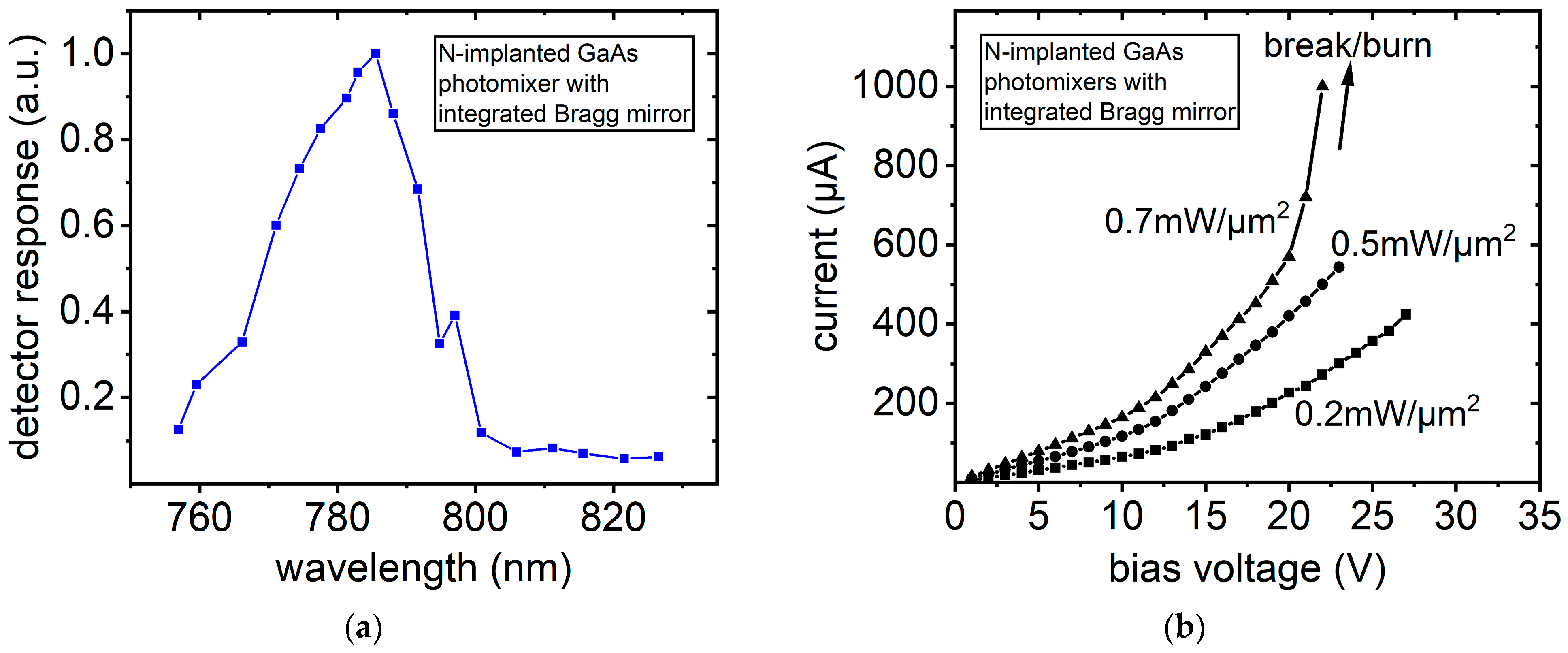
3.2. Carrier Lifetime and Photomixer Characteristics

Besides using Raman spectroscopy to determine the optimal work/operation conditions range, we demonstrate additionally, in this section, that the material system with its carrier lifetime is suitable for the photomixing in devices presented. More details to the photomixer structure performance will be presented in our separate study.
The lifetime of photogenerated carriers in nitrogen-implanted GaAs materials grown on top of the Bragg mirror (Figure 1) was studied using femtosecond, all-optical pump-probe spectroscopy measurements. Details to the setup can be found in [52]. For implanted materials annealed in the range from 300 °C to 400 °C, carrier lifetimes were extracted from the pump-probe data using a bi-exponential fitting based on the Drude model [52]. The initial fast component τ1 represents a sub-picosecond trapping time of hot electrons and was in the range from ~200 to up to 300 fs, respectively. A subsequent “slow” carrier lifetime component τ2, corresponding to the electron–hole recombination time [63], was in the range between 1.2 and 1.4 ps. These results, shown in Figure 5a, are fully comparable with the data extracted from measurements performed on annealed N-implanted GaAs materials without the Bragg mirror (Figure 5b) [64]. The latter confirms that the internal Bragg mirror itself does not additionally affect the carrier lifetime in the implanted and annealed active GaAs layer. Furthermore, it was demonstrated that carrier lifetime values can be tuned, via annealing, to the values best suited for the pre-defined THz output frequency range [65].
In the following, comprehensive THz photomixing experiments were performed on the photomixer presented in Figure 2 with integrated interdigitated MSM structure, dipole antenna, and RF choke (further details will be presented in our separate study). The photomixing results presented in Figure 6a demonstrate the THz output power dependence on the one incident optical wavelength, while the other beam wavelength is shifted by 1 nm, measured by a pyroelectric detector in the wavelength range ~750 nm to 830 nm. A maximum detector response was observed when the wavelengths of the two tunable sources were set to 785 and 786 nm and the total optical power density levels were kept below 0.4 mW/µm2 during the photomixing measurements. The measured detector response maximum (Figure 6a) in this case corresponds to an output frequency of 486 GHz, for which our dipole resonant antenna and our Bragg mirror (calculated reflectivity maximum ~780 nm ÷ 790 nm) were designed. Indeed, these data are in good agreement with the range predicted previously by a simulation of the reflectivity for 12 periods of a GaAs/AlAs superlattice with thicknesses of 55 nm/67 nm, which was presented for MBE grown LT-GaAs materials used for the fabrication of photodetectors and photomixers [66]. Furthermore, representative (total) current-voltage characteristics (Figure 6b) measured on the photomixer structure (after 100 min optical exposure) indicate deviations from a linear behavior for the input optical power density range ~0.7 mW/µm2. This result correlates and is in very good agreement with the data presented in Figure 3b, where the Raman A1g (LO) mode of GaAs exhibits a shift down to about 289 cm−1 for the sample exposed optically for 100 min. Additionally, thermal degradation in the photomixer (MSM) active region was confirmed both by microscope inspection as well as by micro-Raman mapping measurements (Figure 4b) for higher optical power density levels above 0.7 mW/µm2.

4. Discussion

It is well-known that the temperature dependence of the phonon frequency is described by the anharmonic terms in the vibrational Hamiltonian of the crystal lattice, which take into account thermal expansion of the lattice and phonon-phonon interaction [67]. This leads to a red/down shift of the phonon frequency with respect to the harmonic frequency. Further contributions are to be considered for heteroepitaxial systems such as GaAs/Si, when lattice and thermal mismatches cause strain in the epilayer. Here, the temperature dependence of the A1g (LO) frequency mode shift can be analyzed by considering three contributions: the lattice thermal expansion Δ(1)(T), the anharmonic decay of phonons Δ(2)(T), and the strain in the layers Δ(3)(T), as follows [68]:
ω(T) = ω(0) + Δ(1)(T) + Δ(2)(T) + Δ(3)(T),
where ω(0) is the harmonic frequency of the optical mode.
In our experiments, however, we do not concern ourselves with the temperature dependence, but rather with the determination of the effect of optical power density (after exposure) on the Raman shift. The increase of the incident optical power density in our experiments in the range from ~0.02 up to ~1 mW/µm2 leads to the observed “red/down” shift of the Raman band at ~291 cm−1 (A1g (LO)). Therefore, the dependence can be described empirically by the following equation:
ω(PDENS) = ω(NON-EXP) + Χ × PDENS,
where ω(NON-EXP) corresponds to Raman shift before exposure and ω(PDENS) is the experimentally evaluated Raman shift induced by the incident optical power density PDENS. The slope of the fitted characteristics represents the value of Χ. The coefficient Χ depends strongly on the exposure time, i.e., the total time during which the active area of the photomixer structure was illuminated with the incident laser wavelength (780 nm). The values are found to be approx. −1.8, −2.8, and −3.5, for the exposure times 10, 100, and 1000 min, respectively. There is a slight dispersion in the measured values, which deviate from the behavior described by our Equation (2). It can be explained by the measurement procedure, i.e., the “step-by-step” exposure and the successive Raman measurement, which may have affected the characteristics measured. A further optimization of the characterization procedure will be the object of future studies.
In a simple approximation, it can be assumed that the implanted GaAs layer absorbs the laser energy (during the laser exposure) and its surface temperature increases. The initiation of non-reversible degradation processes manifested by melting is taken as a criterion for the thermal damage threshold. In the case of GaAs irradiated with our cw laser operated at 780 nm wavelength during 1, 10, 100, and 1000 min, we were able to monitor “structural” changes in the optical power density range from ~0.02 up to ~1 mW/µm2 with the help of Raman spectroscopy. The major aim of our investigations was to identify the “safe” optical power density region where the material properties do not degrade. Indeed, the presented micro-Raman spectra indicate the initiation of degradation effects (i.e., melting effects/thermal damage threshold) in the investigated structures already at optical power density levels far below <1 mW/µm2. From data reported in the past, we estimated optical power density levels in the range from ~0.125 mW/µm2 [3], ~0.25 mW/µm2 [4], ~0.38 mW/µm2 [8] to ~0.4 mW/µm2 [5], which fully correspond to “safe” optical power density levels as was experimentally determined in our study. Furthermore, power density levels in the range from ~0.62 mW/µm2 [18], ~0.67 mW/µm2 [24,26], ~0.7 mW/µm2 [12] to ~0.8 mW/µm2 [19] were estimated for different photomixer devices, for which no indications of the thermal damage threshold were reported. Nevertheless, e.g., ~2 mW/µm2 [30], and ~2.4 mW/µm2 [13] exceed the “safe” optical power density level range determined in our work, most probably due to enhanced heat dissipation in the structures presented.
In addition, it should be noted that the thermal damage threshold in the implanted GaAs material under investigation occurs for higher bias voltage already at “lower” optical power densities. This is “general knowledge” and was experimentally confirmed for LT-GaAs photomixer structures by numerous groups in the past. Nevertheless, the results presented in our study—especially those “Raman shift vs. power density” measurements presented in Figure 3b—can help find the “safe” operation region for reliable and stable THz generation. A repetition of the “short-term” (100 and 1000 min under ~0.7 and ~0.6 mW/µm2 optical power densities) optical exposure experiments on the THz photomixer structures under investigation, where the Raman A1g (LO) mode of GaAs exhibits shift values below 289 cm−1, confirm the non-reversible “characteristics” of the thermally initialized degradation effects. Finally, our photomixer structures were tested also in the regime of “long-term operation” (up to 1000 h) at “safe” optical power density ~0.4 mW/µm2 at 10 V bias voltage. In the following, the investigated structures were inspected both by optical microscopy as well as by micro-Raman mapping measurements. A comparison of the micro-Raman mapping images (measurements performed over a large MSM active area) before and after long-term operation reveals that the Raman A1g (LO) mode of the GaAs shift stays above 289 cm−1, i.e., the value we determined experimentally below which thermal damage is observed. Nevertheless, this confirms that the photomixer structures can withstand operation up to 1000 h if an average optical power density of ~0.4 mW/µm2 and bias voltage 10 V are kept constant. Hence, the estimation of “safe” operation conditions with the help of Raman spectroscopy can deliver important information for the increase in device “lifetime” and reliability.

5. Conclusions

In this work, we investigated the “evolution” of degradation effects in THz photomixer structures fabricated on nitrogen-implanted GaAs with the help of Raman spectroscopy. The occurrences of the thermal damage threshold/irreversible structural changes were determined and observed for optical power density levels above ~0.6 and ~0.7 mW/µm2 for 1000 and 100 min of operation mode, respectively. In addition, the so-called “safe” optical power density regions were identified. Device testing in the “long-term operation” regime (up to 1000 h) reveals that the photomixer structures can withstand an average optical power density of up to ~0.4 mW/µm2 when biased at 10 V without any indications of degradation. This knowledge is a prerequisite for device applications where device stability, long-term and reliable operation are required. Therefore, Raman spectroscopy will play an important role in the development of “next generation” long-term operating continuous wave THz photomixers.

Author Contributions

Conceptualization, M.M., H.H.H., R.A. and R.S.; methodology, M.M., H.H.H., R.A., G.C., D.C., J.C., I.K., J.S. and S.P.; software, G.C. and D.C.; validation, M.M., H.H.H., R.A., D.E.B., S.F.H., I.K., R.S., J.S. and S.P.; formal analysis, G.C., J.C., D.C. and J.S.; investigation, M.M., H.H.H., R.A., D.E.B., S.F.H., G.C., A.P., J.C., D.C., I.K. and J.S.; resources, J.M., C.M.S., S.P. and R.S., data curation, M.M., H.H.H. and R.S.; writing—original draft, M.M. and H.H.H.; writing—review and editing, M.M., H.H.H., R.A., D.E.B., C.M.S. and R.S.; supervision, H.H.H., J.M., C.M.S., S.P. and R.S.; project administration, S.P. and R.S.; funding acquisition, S.P. and R.S. All authors have read and agreed to the published version of the manuscript.

Funding

Research in Rochester was supported in part by the U.S. Department of Energy under Grant DE-SC0021468.

Data Availability Statement

Experimental data are available upon reasonable request from the corresponding authors.

Conflicts of Interest

The authors declare no conflict of interest. The funders had no role in the design of the study; in the collection, analyses, or interpretation of data; in the writing of the manuscript, or in the decision to publish the results.

References

  1. Liliental-Weber, Z.; Swider, W.; Yu, K.M.; Kortright, J.; Smith, F.W.; Calawa, A.R. Breakdown of crystallinity in low-temperature-grown GaAs layers. Appl. Phys. Lett. 1991, 58, 2153–2155. [Google Scholar] [CrossRef]
  2. Look, D.C. Molecular beam epitaxial GaAs grown at low temperatures. Thin Solid Films 1993, 231, 61–73. [Google Scholar] [CrossRef]
  3. Brown, E.R.; McIntosh, K.A.; Nichols, K.B.; Dennis, C.L. Photomixing up to 3.8 THz in low-temperature-grown GaAs. Appl. Phys. Lett. 1995, 66, 285–287. [Google Scholar] [CrossRef]
  4. McIntosh, K.A.; Brown, E.R.; Nichols, K.B.; McMahon, O.B.; DiNatale, W.F.; Lyszczarz, T.M. Terahertz photomixing with diode lasers in low-temperature-grown GaAs. Appl. Phys. Lett. 1995, 67, 3844–3846. [Google Scholar] [CrossRef]
  5. Matsuura, S.; Tani, M.; Sakai, K. Generation of coherent terahertz radiation by photomixing in dipole photoconductive antennas. Appl. Phys. Lett. 1997, 70, 559–561. [Google Scholar] [CrossRef]
  6. Kordoš, P.; Förster, A.; Marso, M.; Rüders, F. 550 GHz bandwidth photodetector on low-temperature grown molecular-beam epitaxial GaAs. Electron. Lett. 1998, 34, 119–120. [Google Scholar] [CrossRef]
  7. Shan, W.; Yu, K.M.; Walukiewicz, W.; Ager, J.W.; Haller, E.E.; Ridgway, M.C. Reduction of band-gap energy in GaNAs and AlGaNAs synthesized by N+ implantation. Appl. Phys. Lett. 1999, 75, 1410–1412. [Google Scholar] [CrossRef]
  8. Matsuura, S.; Blake, G.A.; Wyss, R.A.; Pearson, J.C.; Kadow, C.; Jackson, A.W.; Gossard, A.C. Design and characterization of optical-THz phase-matched traveling-wave photomixers. In Proceedings of the SPIE’s International Symposium on Optical Science, Engineering, and Instrumentation, Denver, CO, USA, 12 November 1999; Hwu, R.J., Wu, K., Eds.; Terahertz Gigahertz Photonics. Society of Photo-Optical Instrumentation Engineers (SPIE): Bellingham, WA, USA, 1999; p. 484. [Google Scholar] [CrossRef]
  9. Siebert, K.; Siebe, F.; Roskos, H.; Leonhardt, R. A two-color Ti:sapphire laser for CW-THz generation. In Proceedings of the Conference on Lasers and Electro-Optics (CLEO 2000), Technical Digest; Postconference Edition; TOPS Vol.39 (IEEE Cat. No.00CH37088), San Francisco, CA, USA, 7–12 May 2000; p. 497. [Google Scholar] [CrossRef]
  10. Stöhr, A.; Heinzelmann, R.; Hagedorn, K.; Güsten, R.; Schäfer, F.; Stüer, H.; Siebe, F.; van der Wal, P.; Krozer, V.; Feiginov, M.; et al. Integrated 460 GHz photonic transmitter module. Electron. Lett. 2001, 37, 1347–1348. [Google Scholar] [CrossRef]
  11. Yu, K.M.; Walukiewicz, W.; Wu, J.; Beeman, J.W.; Ager, J.W.; Haller, E.E.; Shan, W.; Xin, H.P.; Tu, C.W.; Ridgway, M.C. Formation of diluted III–V nitride thin films by N ion implantation. J. Appl. Phys. 2001, 90, 2227–2234. [Google Scholar] [CrossRef]
  12. Mikulics, M.; Siebe, F.; Fox, A.; Marso, M.; Forster, A.; Stuer, H.; Schafer, F.; Gusten, R.; Kordos, P. Generation of 460 GHz radiation by photomixing in low-temperature-grown MBE GaAs. In Proceedings of the Fourth International Conference on Advanced Semiconductor Devices and Microsystem, Smolenice, Slovakia, 16 October 2003. [Google Scholar] [CrossRef]
  13. Peytavit, E.; Arscott, S.; Lippens, D.; Mouret, G.; Matton, S.; Masselin, P.; Bocquet, R.; Lampin, J.F.; Desplanque, L.; Mollot, F. Terahertz frequency difference from vertically integrated low-temperature-grown GaAs photodetector. Appl. Phys. Lett. 2002, 81, 1174–1176. [Google Scholar] [CrossRef]
  14. Wu, J.; Shan, W.; Walukiewicz, W. Band anticrossing in highly mismatched III V semiconductor alloys. Semicond. Sci. Technol. 2002, 17, 860–869. [Google Scholar] [CrossRef]
  15. Mikulics, M.; Marso, M.; Kordoš, P.; Stanček, S.; Kováč, P.; Zheng, X.; Wu, S.; Sobolewski, R. Ultrafast and highly sensitive photodetectors fabricated on high-energy nitrogen-implanted GaAs. Appl. Phys. Lett. 2003, 83, 1719–1721. [Google Scholar] [CrossRef]
  16. Sinning, S.; Dekorsy, T.; Helm, M. Ultrafast carrier dynamics in nitrogen-implanted GaAs. IEE Proc. Optoelectron. 2004, 151, 361–364. [Google Scholar] [CrossRef]
  17. Krotkus, A.; Coutaz, J.-L. Non-stoichiometric semiconductor materials for terahertz optoelectronics applications. Semicond. Sci. Technol. 2005, 20, S142–S150. [Google Scholar] [CrossRef]
  18. Döhler, G.H.; Renner, F.; Klar, O.; Eckardt, M.; Schwanhäußer, A.; Malzer, S.; Driscoll, D.; Hanson, M.; Gossard, A.C.; Loata, G.; et al. THz-photomixer based on quasi-ballistic transport. Semicond. Sci. Technol. 2005, 20, S178–S190. [Google Scholar] [CrossRef]
  19. Mikulics, M.; Marso, M.; Mayorga, I.C.; Güsten, R.; Stanček, S.; Kováč, P.; Wu, S.; Li, X.; Khafizov, M.; Sobolewski, R.; et al. Photomixers fabricated on nitrogen-ion-implanted GaAs. Appl. Phys. Lett. 2005, 87, 041106. [Google Scholar] [CrossRef]
  20. Suzuki, M.; Tonouchi, M. Fe-implanted InGaAs photoconductive terahertz detectors triggered by 1.56μm femtosecond optical pulses. Appl. Phys. Lett. 2005, 86, 163504. [Google Scholar] [CrossRef]
  21. Salem, B.; Morris, D.; Aimez, V.; Beerens, J.; Beauvais, J.; Houde, D. Pulsed photoconductive antenna terahertz sources made on ion-implanted GaAs substrates. J. Physics Condens. Matter 2005, 17, 7327–7333. [Google Scholar] [CrossRef]
  22. Chimot, N.; Mangeney, J.; Joulaud, L.; Crozat, P.; Bernas, H.; Blary, K.; Lampin, J.F. Terahertz radiation from heavy-ion-irradiated In0.53Ga0.47As photoconductive antenna excited at 1.55 μm. Appl. Phys. Lett. 2005, 87, 193510. [Google Scholar] [CrossRef]
  23. Mikulics, M.; Wu, S.; Marso, M.; Adam, R.; Forster, A.; van der Hart, A.; Kordos, P.; Luth, H.; Sobolewski, R. Ultrafast and highly sensitive photodetectors with recessed electrodes fabricated on low-temperature-grown GaAs. IEEE Photon. Technol. Lett. 2006, 18, 820–822. [Google Scholar] [CrossRef]
  24. Mikulics, M.; Michael, E.A.; Schieder, R.; Stutzki, J.; Güsten, R.; Marso, M.; van der Hart, A.; Bochem, H.P.; Lüth, H.; Kordoš, P. Traveling-wave photomixer with recessed interdigitated contacts on low-temperature-grown GaAs. Appl. Phys. Lett. 2006, 88, 041118. [Google Scholar] [CrossRef]
  25. Salem, B.; Morris, D.; Aimez, V.; Beauvais, J.; Houde, D. Improved characteristics of a terahertz set-up built with an emitter and a detector made on proton-bombarded GaAs photoconductive materials. Semicond. Sci. Technol. 2006, 21, 283–286. [Google Scholar] [CrossRef]
  26. Mikulics, M.; Michael, E.A.; Marso, M.; Lepsa, M.; van der Hart, A.; Lüth, H.; Dewald, A.; Stanček, S.; Mozolik, M.; Kordoš, P. Traveling-wave photomixers fabricated on high energy nitrogen-ion-implanted GaAs. Appl. Phys. Lett. 2006, 89, 071103. [Google Scholar] [CrossRef]
  27. Sartorius, B.; Roehle, H.; Künzel, H.; Böttcher, J.; Schlak, M.; Stanze, D.; Venghaus, H.; Schell, M. All-fiber terahertz time-domain spectrometer operating at 1.5 μm telecom wavelengths. Opt. Express 2008, 16, 9565–9570. [Google Scholar] [CrossRef]
  28. Ospald, F.; Maryenko, D.; von Klitzing, K.; Driscoll, D.C.; Hanson, M.P.; Lu, H.; Gossard, A.C.; Smet, J.H. 1.55 μm ultrafast photoconductive switches based on ErAs: InGaAs. Appl. Phys. Lett. 2008, 92, 131117. [Google Scholar] [CrossRef]
  29. Mikulics, M.; Marso, M.; Wu, S.; Fox, A.; Lepsa, M.; Grutzmacher, D.; Sobolewski, R.; Kordos, P. Sensitivity Enhancement of Metal– Semiconductor –Metal Photodetectors on Low-Temperature-Grown GaAs Using Alloyed Contacts. IEEE Photonics Technol. Lett. 2008, 20, 1054–1056. [Google Scholar] [CrossRef]
  30. Peytavit, E.; Lampin, J.-F.; Hindle, F.; Yang, C.; Mouret, G. Wide-band continuous-wave terahertz source with a vertically integrated photomixer. Appl. Phys. Lett. 2009, 95, 161102. [Google Scholar] [CrossRef]
  31. Plinski, E. Terahertz photomixer. Bull. Pol. Acad. Sci. Tech. Sci. 2010, 58, 463–470. [Google Scholar] [CrossRef]
  32. Hofmann, M.R.; Scheller, M.; Brenner, C.; Baaske, K.; Koch, M. Cost-effective THz spectroscopy with continuous-wave laser sources. In Proceedings of the EuCAP 2010—4th European Conference on Antennas and Propagation, Barcelona, Spain, 12–16 April 2010; pp. 1–4. [Google Scholar]
  33. Pačebutas, V.; Bičiūnas, A.; Balakauskas, S.; Krotkus, A.; Andriukaitis, G.; Lorenc, D.; Pugžlys, A.; Baltuška, A. Terahertz time-domain-spectroscopy system based on femtosecond Yb:fiber laser and GaBiAs photoconducting components. Appl. Phys. Lett. 2010, 97, 031111. [Google Scholar] [CrossRef]
  34. Preu, S.; Döhler, G.H.; Malzer, S.; Wang, L.J.; Gossard, A.C. Tunable, continuous-wave Terahertz photomixer sources and applications. J. Appl. Phys. 2011, 109, 061301. [Google Scholar] [CrossRef]
  35. Brenner, C.; Friedrich, C.-S.; Hofmann, M.R. Semiconductor Diode Lasers for Terahertz Technology. J. Infrared. Millimeter. Terahertz Waves 2011, 32, 1253–1266. [Google Scholar] [CrossRef]
  36. Xu, M.; Mittendorff, M.; Dietz, R.J.B.; Künzel, H.; Sartorius, B.; Göbel, T.; Schneider, H.; Helm, M.; Winnerl, S. Terahertz generation and detection with InGaAs-based large-area photoconductive devices excited at 1.55 μm. Appl. Phys. Lett. 2013, 103, 251114. [Google Scholar] [CrossRef]
  37. Koenig, S.; Lopez-Diaz, D.; Antes, J.; Boes, F.; Henneberger, R.; Leuther, A.; Tessmann, A.; Schmogrow, R.; Hillerkuss, D.; Palmer, R.; et al. Wireless sub-THz communication system with high data rate. Nat. Photonics 2013, 7, 977–981. [Google Scholar] [CrossRef]
  38. Deninger, A. State-of-the-art in terahertz continuous-wave photomixer systems. In Handbook of Terahertz Technology for Imaging, Sensing and Communications; Elsevier: Amsterdam, The Netherlands, 2013; pp. 327–373. [Google Scholar] [CrossRef]
  39. Peytavit, E.; Pavanello, F.; Ducournau, G.; Lampin, J.-F. Highly efficient terahertz detection by optical mixing in a Fabry-Perot cavity LT-GaAs photoconductor. In Proceedings of the 2014 39th International Conference on Infrared, Millimeter, and Terahertz Waves (IRMMW-THz), Tucson, AZ, USA, 14–19 September 2014; pp. 1–2. [Google Scholar] [CrossRef]
  40. Ríos, R.D.V.; Bikorimana, S.; Ummy, M.A.; Dorsinville, R.; Seo, S.-W. A bow-tie photoconductive antenna using a low-temperature-grown GaAs thin-film on a silicon substrate for terahertz wave generation and detection. J. Opt. 2015, 17, 125802. [Google Scholar] [CrossRef]
  41. Nagatsuma, T.; Ducournau, G.; Renaud, C.C. Advances in terahertz communications accelerated by photonics. Nat. Photonics 2016, 10, 371–379. [Google Scholar] [CrossRef]
  42. Currie, M. Low-temperature grown Gallium Arsenide (LT-GaAs) high-speed detectors. In Photodetectors; Elsevier: Amsterdam, The Netherlands, 2016; pp. 121–155. [Google Scholar] [CrossRef]
  43. Burford, N.M.; El-Shenawee, M.O. Review of terahertz photoconductive antenna technology. Opt. Eng. 2017, 56, 010901. [Google Scholar] [CrossRef]
  44. Kohlhaas, R.B.; Dietz, R.J.B.; Breuer, S.; Nellen, S.; Liebermeister, L.; Schell, M.; Globisch, B. Improving the dynamic range of InGaAs-based THz detectors by localized beryllium doping: Up to 70 dB at 3 THz. Opt. Lett. 2018, 43, 5423–5426. [Google Scholar] [CrossRef] [PubMed]
  45. Ponomarev, D.; Lavrukhin, D.; Yachmenev, A.; Khabibullin, R.; Semenikhin, I.; Vyurkov, V.; Ryzhii, M.; Otsuji, T.; Ryzhii, V. Sn-nanothreads in GaAs matrix and their sub- and terahertz applications. J. Phys. Conf. Ser. 2018, 1092, 012166. [Google Scholar] [CrossRef]
  46. Safian, R.; Ghazi, G.; Mohammadian, N. Review of photomixing continuous-wave terahertz systems and current application trends in terahertz domain. Opt. Eng. 2019, 58, 110901. [Google Scholar] [CrossRef]
  47. Che, M.; Matsuo, Y.; Kanaya, H.; Ito, H.; Ishibashi, T.; Kato, K. Optoelectronic THz-Wave Beam Steering by Arrayed Photomixers with Integrated Antennas. IEEE Photonics Technol. Lett. 2020, 32, 979–982. [Google Scholar] [CrossRef]
  48. Xie, J.; Ye, W.; Zhou, L.; Guo, X.; Zang, X.; Chen, L.; Zhu, Y. A Review on Terahertz Technologies Accelerated by Silicon Photonics. Nanomaterials 2021, 11, 1646. [Google Scholar] [CrossRef] [PubMed]
  49. Che, M.; Kondo, K.; Kanaya, H.; Kato, K. Arrayed Photomixers for THz Beam-Combining and Beam-Steering. J. Light. Technol. 2022, 40, 6657–6665. [Google Scholar] [CrossRef]
  50. Hollfelder, M.; Hardtdegen, H.; Meyer, R.; Carius, R.; Lüth, H. (AlGa)As grown by low pressure metalorganic vapor phase epitaxy using a N2 carrier. J. Electron. Mater. 1994, 23, 1061–1065. [Google Scholar] [CrossRef]
  51. Hardtdegen, H.; Ungermanns, C.; Hollfelder, M.; Raafat, T.; Carius, R.; Hasenöhrl, S.; Lüth, H. A new approach towards low-pressure metalorganic vapor phase epitaxy of (AlGa)As using triethylgallium and dimethylethylaminealane. J. Cryst. Growth 1994, 145, 478–484. [Google Scholar] [CrossRef]
  52. Chen, G.; Chakraborty, D.; Cheng, J.; Mikulics, M.; Komissarov, I.; Adam, R.; Bürgler, D.E.; Schneider, C.M.; Hardtdegen, H.; Sobolewski, R. Transient THz Emission and Effective Mass Determination in Highly Resistive GaAs Crystals Excited by Femtosecond Optical Pulses. Crystals 2022, 12, 1635. [Google Scholar] [CrossRef]
  53. Mikulics, M.; Lu, J.; Huang, L.; Tse, P.; Zhang, J.; Mayer, J.; Hardtdegen, H. Laser micro annealing conditioning for the suppression of statistical scatter in freestanding Sb2Te3 nanowire resistance. Flatchem 2020, 21, 100164. [Google Scholar] [CrossRef]
  54. Wagner, J.; Hoffman, C. Resonant two-phonon Raman scattering in GaAs: A sensitive probe for implantation damage and annealing. Appl. Phys. Lett. 1987, 50, 682–684. [Google Scholar] [CrossRef]
  55. Fleischer, S.; Beling, C.D.; Fung, S.; Nieveen, W.R.; Squire, J.E.; Zheng, J.Q.; Missous, M. Structural and defect characterization of GaAs and AlxGa1−xAs grown at low temperature by molecular beam epitaxy. J. Appl. Phys. 1997, 81, 190–198. [Google Scholar] [CrossRef]
  56. Jiang, D.-S.; Li, X.-P.; Sun, B.-Q.; Han, H.-X. A Raman scattering study of GaAs: As films lifted off GaAs substrate. J. Phys. D Appl. Phys. 1999, 32, 629–631. [Google Scholar] [CrossRef]
  57. Yazji, S.; Zardo, I.; Soini, M.; Postorino, P.; Morral, A.F.i.; Abstreiter, G. Local modification of GaAs nanowires induced by laser heating. Nanotechnology 2011, 22, 325701. [Google Scholar] [CrossRef]
  58. McDevitt, N.T.; Baun, W.L.; Solomon, J.S. Characterization of Thermally Treated Gallium Arsenide by Laser-Raman and Auger Spectroscopy. 1984. Available online: https://apps.dtic.mil/sti/tr/pdf/ADA148414.pdf (accessed on 8 August 2023).
  59. McDevitt, N.T.; Solomon, J.S. Thermal Oxide Layers on GaAs Studied by Raman and Auger Spectroscopy. J. Electrochem. Soc. 1986, 133, 1913–1917. [Google Scholar] [CrossRef]
  60. Garg, A.; Kapoor, A.; Tripathi, K. Laser-induced damage studies in GaAs. Opt. Laser Technol. 2003, 35, 21–24. [Google Scholar] [CrossRef]
  61. Pimenta, A.C.S.; Limborço, H.; González, J.C.; Cifuentes, N.; Ramos, S.L.L.M.; Matinaga, F.M. Photodegradation of Si-doped GaAs nanowire. RSC Adv. 2019, 9, 39488–39494. [Google Scholar] [CrossRef] [PubMed]
  62. Pizani, P.S.; Campos, C.E.M. Raman probing of thermal damage depth profile in annealed GaAs. J. Appl. Phys. 1998, 84, 6588–6591. [Google Scholar] [CrossRef]
  63. Shockley, W.; Read, W.T. Statistics of the Recombinations of Holes and Electrons. Phys. Rev. 1952, 87, 835–842. [Google Scholar] [CrossRef]
  64. Mikulics, M.; Marso, M.; Mantl, S.; Lüth, H.; Kordoš, P. GaAs photodetectors prepared by high-energy and high-dose nitrogen implantation. Appl. Phys. Lett. 2006, 89, 091103. [Google Scholar] [CrossRef]
  65. Chen, G.; Mikulics, M.; Adam, R.; Pericolo, A.; Serafini, J.; Preble, S.; Cheng, J.; Chimera, C.; Komissarov, I.; Hardtdegen, H.H.; et al. Photomixing THz Generation from Nitrogen-Ion–Implanted GaAs Metal-Semiconductor-Metal Diodes Enhanced by a Bragg Mirror. In Proceedings of the 2020 45th International Conference on Infrared, Millimeter, and Terahertz Waves (IRMMW-THz), Buffalo, NY, USA, 8–13 November 2020; pp. 1–2. [Google Scholar] [CrossRef]
  66. Mikulics, M. Preparation and Optimization of Low-Temperature Grown GaAs Photomixers. Ph.D. Thesis, RWTH Aachen, Aachen, Germany, 2005. [Google Scholar]
  67. Menéndez, J.; Cardona, M. Temperature dependence of the first-order Raman scattering by phonons in Si, Ge, andα−Sn: Anharmonic effects. Phys. Rev. B 1984, 29, 2051–2059. [Google Scholar] [CrossRef]
  68. Ardila, A.M.; Martínez, O.; Avella, M.; Jiménez, J.; Gérard, B.; Napierala, J.; Gil-Lafon, E. Temperature dependence of the Raman shift in GaAs conformal layers grown by hydride vapor phase epitaxy. J. Appl. Phys. 2002, 91, 5045–5050. [Google Scholar] [CrossRef]
Figure 1. SEM micrograph of the AlAs/GaAs layers serving as a Bragg mirror and grown by MOVPE on SI-GaAs. The contrast was increased by etching the AlAs layers with an HF-H2O (1:40) solution. An AlAs/GaAs Bragg mirror with nominal thicknesses (before etching) of 67 nm/55 nm was chosen for the MOVPE epitaxial layer growth.
Crystals 13 01267 g001
Figure 2. (a) Optical micrograph of an MSM structure (b) integrated with a resonant dipole antenna and RF choke.
Crystals 13 01267 g002
Figure 3. (a) representative Raman spectra collected in the central area of the interdigitated MSM structure (THz photomixer) for the non-exposed (blue) and exposed (red) areas. (b) position of the Raman A1g (LO) mode for nitrogen-implanted GaAs as a function of incident optical power density (wavelength 780 nm) for different exposure times (texp) and constant 10 V bias. Each data point was achieved by recording a Raman spectrum after exposing the material for the exposure time texp at the respective power density. The dashed lines through the measurement data are only a guide to the eye. Please note that four different photomixer structures were used for the respective measurements. Although the structures were fabricated on the identical material, the individual lithographical imperfections (see Figure 4a,b) can influence heat dissipation processes differently. Therefore, the slope could deviate slightly from that expected.
Crystals 13 01267 g003
Figure 4. Exemplary micro-Raman intensity mapping images for the Raman mode at 289 cm−1 with data collected in the central area of the interdigitated MSM structure (a) without indication of degradation/thermal damage; (b) with indication of local degradation/thermal damage. The mapping images were obtained with the help of Renishaw software (version 5.2). The intensity at 289 cm−1 is color coded from red for low to yellow for high intensity.
Crystals 13 01267 g004
Figure 5. Comparison of normalized reflectivity change (representative) measurements for N-implanted SI GaAs materials with (a) and without (b) integrated Bragg mirror. (a) samples annealed at 300 °C, 350 °C, and 400 °C [52]; (b) samples annealed at 300 °C, 400 °C, and 600 °C reproduced from [Mikulics, M.; Marso, M.; Mantl, S.; Lüth, H.; Kordoš, P. GaAs photodetectors prepared by high-energy and high-dose nitrogen implantation. Appl. Phys. Lett. 2006, 89, 091103. https://doi.org/10.1063/1.2339907] with the permission of AIP Publishing.
Crystals 13 01267 g005
Figure 6. (a) example for normalized detector response (sample annealed at 300 °C) versus wavelength of both cw laser sources, whereat their relative difference is kept constant and equal to 1 nm. The x-axis corresponds to the wavelength of only one of the laser sources. (b) exemplary IV characteristics for a THz photomixer sample (after a 100 min exposure time) measured at different optical power densities.
Crystals 13 01267 g006
Disclaimer/Publisher’s Note: The statements, opinions and data contained in all publications are solely those of the individual author(s) and contributor(s) and not of MDPI and/or the editor(s). MDPI and/or the editor(s) disclaim responsibility for any injury to people or property resulting from any ideas, methods, instructions or products referred to in the content.

