1. Introduction
Thin film solar cells have gained extensive attention owing to their advantages such as their high efficiency, low cost, and flexibility. In order to further reduce the price of thin film solar cells and improve their application value, absorbing layer materials as Cu
2ZnSnS
4 (CZTS), Sb
2S
3, CuSbS
2, and CuPbSbS
3, which have abundant element reserves and good photoelectric performance, have attracted more and more attention from researchers [
1]. In CZTS thin film, multiple defects are easy to form, and the secondary phases of N-type semiconductors such as ZnS and SnS
2 make it easy to affect the device’s efficiency [
2,
3]. Sb
2S
3 is a quasi-one-dimensional structural material, and its crystal orientation is complex and difficult to adjust, which will seriously affect the charge transfer efficiency [
4]. CuSbS
2 is a two-dimensional material, and the 2D monolayered crystal structure prevents the overlap of the electron clouds between the layers, allowing efficient transportation of the carriers in an intra-layer manner but blocking their transportation along the out-of-plane direction [
5]. Recently, some pioneering works have shown that the introduction of Pb source into CuSbS
2 to form CuPbSbS
3 can improve the two-dimensional crystal structure to a three-dimensional crystal. The three-dimensional electron cloud structure will help improve the charge transfer efficiency, which is expected to demonstrate advanced electronic dimensionality [
6].
The first appearance of CuPbSbS
3 in solar cells was a top structure device of Glass/ITO/CdS/CuPbSbS
3/Spiro-OMeTAD/Au prepared by Professor Tang’s group using the spin-coating method. This device achieved a photoelectric conversion efficiency (PCE) of 2.23% and an open voltage (V
OC) of 699 mV [
6]. Subsequently, they further updated the PCE to 2.65% in 2021 by optimizing the crystallinity of the CuPbSbS
3 film, which is also the champion device efficiency of CuPbSbS
3 so far [
7].
The preparation method of CuPbSbS
3 and its application in solar cells are relatively not enough. The common preparation method for similar four-component compound CZTS films is the solution-spin coating method, which can easily control the content of each component and form a film with uniform texture and controllable thickness. However, since the K
sp of PbS, Sb
2S
3, and Cu
2S are too different with respect to orders of magnitude, it is difficult to prepare CuPbSbS
3 with an aqueous solution-spin coating method. Due to the large number of coordination bonds to be paired on the S atom in butyldithiocarbamic acid (BDCA) solution, it can chelate metal cations very effectively and form a stable gel, finally precipitate the corresponding metal sulfides through high temperature heating [
8,
9]. The above BDCA solution method has achieved great success in the preparation of other photovoltaic absorption materials and its feasibility has been fully verified [
8,
10]. In this regard, we tried to use BDCA solution to prepare the precursor solution. A CuPbSbS
3 film can be formed under the joint reaction of a variety of metal sulfides [
9]. However, in this process, the CuPbSbS
3 film will inevitably undergo relatively complex annealing conditions, which is easy to cause irreversible effects on other functional layers (especially in the top structure solar cell). Consequently, we use chemically stable, electrically conductive, and single-crystal oriented Mo films as substrates, which enables CuPbSbS
3 deposited on Mo substrates to perform more demanding process operations, and also benefits the substrate structure design of CuPbSbS
3 solar cells.
In this article, we have prepared a pure p-type CuPbSbS3 thin film with wide bandgap of 2.0 eV and high absorption coefficient of ~105 cm−1. The characteristics make it a top cell material in laminated cells. In order to further explore its potential of photoelectric device, we have assembled a substrate structured CuPbSbS3 solar cells for the first time. The final assembled device has a photoelectric conversion efficiency of 0.094%. Lastly, we analyzed the adverse factors of the cell performance from the band structure and conductive properties.
3. Results and Discussion
BDCA is easily synthesized by the combination reaction of n-butylamine (CH
3(CH
2)
3NH
2) and carbon disulfide (CS
2), and used to dissolve a variety of metal oxides (MO) to form sulfur-based organometallic complex precursor solutions (reaction 1). The organometallic complex will be pyrolyzed to form the sulfur-based complex (reaction 2).
The Cu-Pb-Sb precursors are subsequently mixed at a mole ratio of Cu:Pb:Sb = 0.9:1:1. In order to explore the formation process of substances and afterwards determine the drying and annealing temperatures of the sintering procedure, TGA and DSC of Cu-Pb-Sb mixed solution was performed.
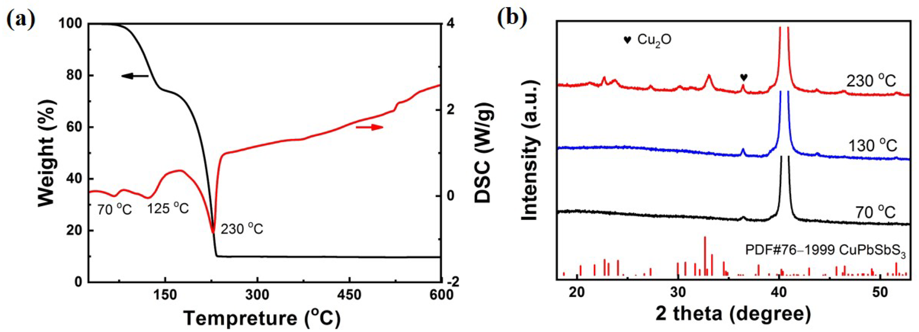
Figure 2a shows the phase change process of the Cu-Pb-Sb mixed solution. The endothermic peak at 70 °C attributes to the evaporation of ethanol. A broad endothermic peak around 125 °C is associated to removal of free BDCA. At 230 °C, the Cu-Pb-Sb mixed solution has the greatest mass loss, owing to the fact that the BDCA solution begins to dissociate the metal sulfides and starts the reaction to form CuPbSbS
3. In order to confirm this hypothesis, XRD tests were conducted on the as-spin coating film annealing at different temperatures. As shown in
Figure 2b, the film shows amorphous properties after annealing at 70 °C, in which the diffraction peak at 36.41° belongs to Cu
2O preferentially precipitated in solution. Due to the small charge and coordination number of Cu
+, its polarization ability is weak, and the coordination bond strength of the coordination compound formed with BDCA solution is also low. Therefore, the precipitation of Cu
2O was observed at 70 °C. The phenomenon of producing a p-type light-absorbing material of copper oxide in the film, which maybe helps to promote the absorption of sunlight, and is also easy to form a copper poor CuPbSbS
3 thin film benefit to improve the device efficiency similar in copper based solar cells, such as Cu(In,Ga)(S,Se)
2 and CZTS. Above situation is consistent with the purpose of the proportion of copper poor elements used in the design of the experiment. The XRD pattern of the sample annealing at 130 °C is consistent with that of 70 °C, which indicates that CuPbSbS
3 cannot be generated in the sample below 125 °C. However, when the temperature was increased to 230 °C, the sample showed obvious multiple diffraction peaks, which belonged to CuPbSbS
3 phase (PDF#76-1999). The Cu-Pb-Sb mixed sulfides dissociates and stable CuPbSbS
3 phase is formed around 230 °C. Based on the above XRD and TG analysis, we can obtain a more suitable preparation process, and set the drying and annealing temperatures of the final film preparation to 70 °C and 275 °C accordingly.
Generally a ~500 nm absorber film is beneficial to photoelectric performance of thin film solar cells [
2]. The thickness of thin film can be easily adjusted by repeating spin-coating/sintering process. Thus, CuPbSbS
3 films were prepared by repeating spin-coating/sintering process. To clarify the formation process of CuPbSbS
3 films by the spin coating method, the morphology, composition, and structural characteristics of each layer were investigated. As shown in
Figure 3, the 1 layer (1L) film is a uniform film with a thickness of about 220 nm, and the grain size is about 60 nm. However, there are some ~100 nm special particles on its surface. After repeating the spin-coating/sintering process, the prepared 2 layers (2L) and 3 layers (3L) films are uniform and dense without the special large particles. The grain sizes of 2L and 3L films are similar to that of 1L film. The thicknesses of 2L and 3L film are 400 nm and 560 nm, respectively.
The energy dispersive spectrometer (EDS) was used to explore the component of 1L, 2L and 3L films. EDS tests were applied at five different points for uniformity test and 100 µm
2 area for average value test. SEM images of CuPbSbS
3 films for the EDS test are presented in
Figure S1 of Supplementary information and the results are summarized in
Table 1. The EDS results of 1L sample shows that the average Cu:Pb:Sb:S ratio of 100 µm
2 area is 1.0:1.4:0.99:4.1, which is slightly different from the 1.0:1.0:1.0:3.0 of chemometric CuPbSbS
3, mainly displaying a Pb-rich and S-rich constituent. We hypothesize that some PbS failed to participate in the reaction to form CuPbSbS
3 while PbS is finally precipitated in BDCA solution. This phenomenon is confirmed in the XRD pattern (
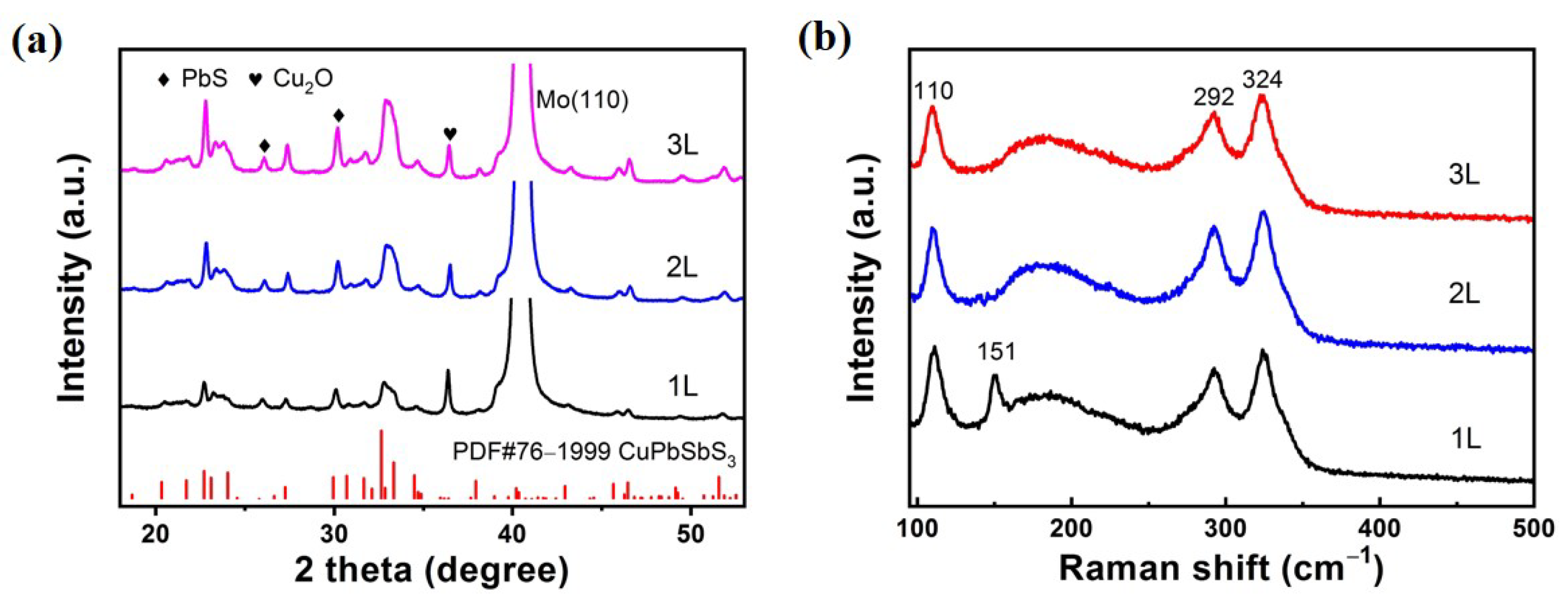
Figure 4a), and the diffraction peaks of PbS are detected in all of the XRD patterns of the films. However, the average element content detected at the positions of large particles of 1L film (point1, 2 and 3) is 1.0:1.5:1.4:4.0, which is different from the average element content of the 100 µm
2 area. On account of the higher Sb and S contents, it can be inferred that the large particles on 1L film maybe Sb
2S
3 grains which was found similarly in the literature [
11]. For the 2L and 3L films, the element content ratios at each position are relatively consistent, which indicates that the prepared films are high uniformity and that the element ratios are close to the chemometric CuPbSbS
3.
In
Figure 4a, the XRD patterns show that the CuPbSbS
3 diffraction peaks of the 2L and 3L films are obviously enhanced and the crystallinity is improved after repeated spin-coating and annealing. With the increase of spin-coating times, Cu
2O and PbS phases still exist, which is consistent with the above conclusion. Since the solubility of Cu
2O in BDCA is not high, it is precipitated easily even though it is annealed at low temperature. PbS is precipitated when BDCA is dissociated at a high temperature. However, there is no diffraction peaks of Sb compound can be detected even in 1L sample, which proves that the content of Sb
2S
3 particles is low. Moreover, it is also found from SEM images that the Sb
2S
3 particles only appear on 1L film, meaning little content of Sb
2S
3 secondaryphase in the film.
To further verify the above results, we conduct Raman tests and show them in
Figure 4b. Raman spectra show that the 1L film annealed at 270 °C has obvious Raman peaks of CuPbSbS
3 phase (110 cm
−1, 292 cm
−1 and 342 cm
−1), which is consistent with the literature [
12]. A 151 cm
−1 peak referred to the Sb
2S
3 phase only appears on 1L film rather than 2L and 3L films, which verifies again the existence of Sb
2S
3 on 1L film except other samples [
13]. These results are in agreement with those of SEM and XRD.
To sum up, we can clearly understand the formation process of CuPbSbS3 film. Firstly, Cu2O is precipitated easily due to volatilization of BDCA solution even at low temperature of 70 °C. Secondly, Sb2S3 and PbS are precipitated when 1L film is spin-coated, but only PbS phase is precipitated in 2L and 3L samples. Finally, a main phase is CuPbSbS3 by annealing above 230 °C. Although the composition of the film is complex, the tiny secondary phases Cu2O, Sb2S3 and PbS are p-type semiconductors and light-absorbing materials similar to CuPbSbS3. Therefore, the existence of these secondary phases may also bring certain performance improvements to solar cells.
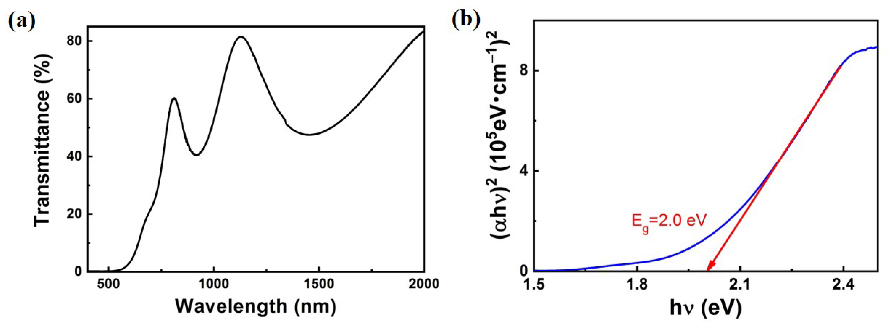
In order to explore the potential of CuPbSbS
3 films as absorption materials, we tested the transmission spectrum and calculated absorption coefficient of a 3L-CuPbSbS
3 film on glass, as shown in
Figure 5. The absorption coefficient of CuPbSbS
3 film can reach up to 10
5 cm
−1, which fully proves its potential as an absorption material for solar cells. The calculated band gap of CuPbSbS
3 is 2.0 eV which is different from its theoretical direct band gap of 1.41 eV [
14]. In fact, due to differences in preparation methods, the actual band gap value reported now will be slightly different. For example, Richard L. Brutchey’s team prepared CuPbSbS
3 with a band gap of 1.21 eV in 2020 [
15]. In the same year, the band gap of CuPbSbS
3 prepared by J. Tang’s team is 1.31 eV [
6]. David J. Lewis’s group prepared CuPbSbS
3 powder with a band gap of 1.55 eV in 2021 [
12]. In the process of preparing CuPbSbS
3, secondary phases such as Cu
2O (2.2–2.48 eV), PbS (0.76–1.91 eV) and Sb
2S
3 (1.7–1.8 eV) are easily generated, and the formation of these secondary phases will have a certain impact on the final band gap of the film [
16,
17,
18,
19,
20]. The wide band gap value of 2.0 eV indicates that CuPbSbS
3 can be applied to the laminated top solar cell material, which helps to improve the light absorption of the laminated solar cell in the short wavelength segment. So, we prepare CuPbSbS
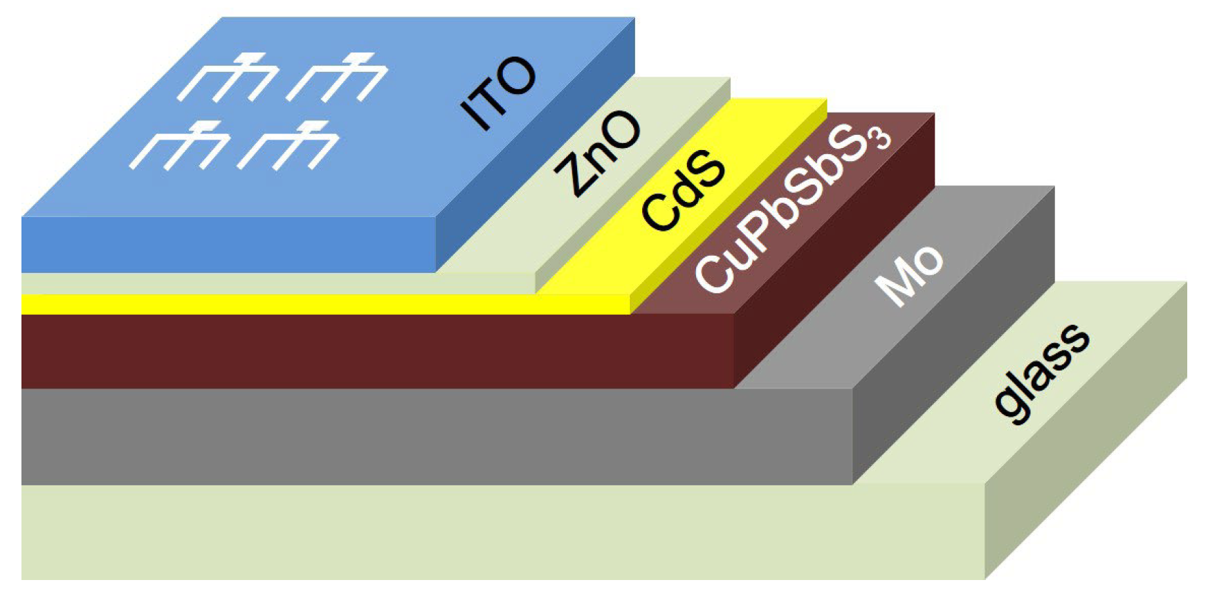
3 films with repeating the spin coating/sintering process three times, and assemble them into Glass/Mo/CuPbSbS
3/CdS/ZnO/ITO structure of the solar cell to probe into its development potential in laminated top solar cells.
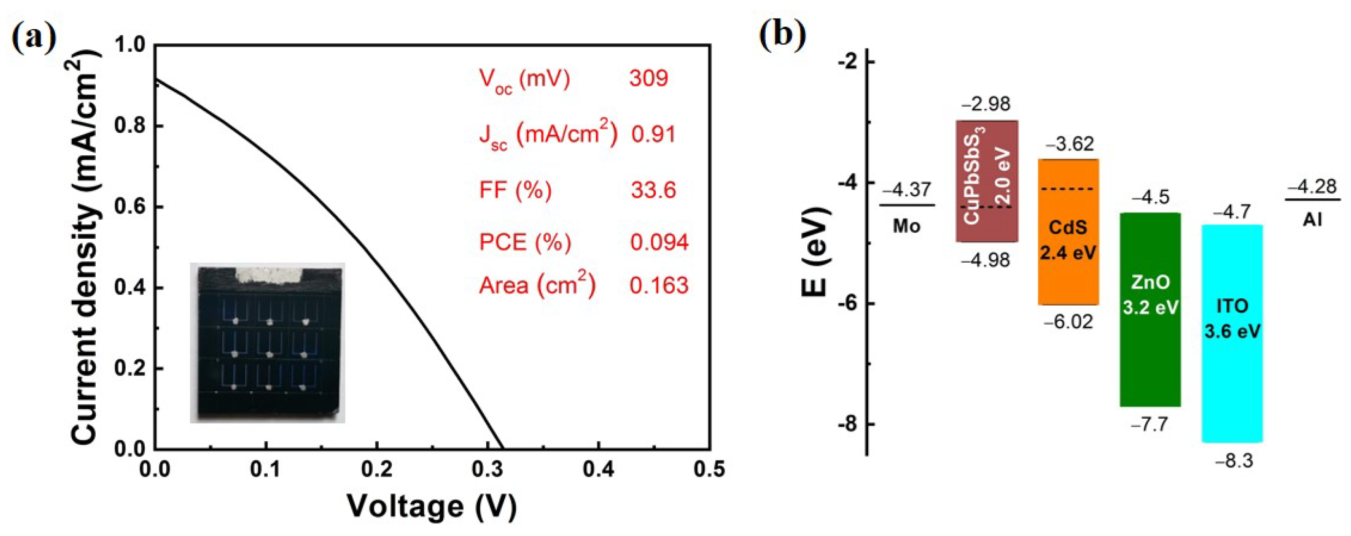
The photovoltaic performance of the device is shown in
Figure 6a. The obtained open voltage (V
OC), short circuit current density (J
SC), filling factor (FF) and PCE of CuPbSbS
3 cell are 309 mV, 0.91 mA/cm
2, 33.6% and 0.094%, respectively. The collection efficiency of photoexcited carriers was tested from the EQE spectrum presented in
Figure S3. The integrating current obtained with EQE spectrum is 0.81 mA/cm
2 which is consistent with the J
SC obtained from J-V curve. To investigate the charge extraction and recombination processes in the solar device, the electrochemical impedance spectroscopy (EIS) experiment was executed under dark conditions, which is displayed in
Figure S4; the corresponding equivalent circuit model is also illustrated. The fitted equivalent circuit model is composed of series resistance (R
s), charge transfer resistance (R
tr), and recombination resistance (R
rec), as well as parallel capacitors of C
tr and C
rec. The fitted R
s, R
tr and R
rec are 36 ohm, 283 ohm and 481 ohm, respectively. The R
rec is inversely proportional to the charge recombination rate of the device. R
rec of the CuPbSbS
3 solar cell is lower than that of the emerging CZTS and Sb
2S
3 solar cells by one order of magnitude, meaning a more recombination loss in our device [
2,
21]. The dark J-V curve of the CuPbSbS
3 device is used to determine the diode properties. As shown in
Figure S5, the reverse saturation current (J
0) is 1.74 × 10
−4 mA/cm
2, which is about two orders of magnitude larger than that of the emerging CZTS and Sb
2S
3 solar cells, indicating that there is an excess of short-circuit channels in the CuPbSbS
3 device [
2,
21]. The existent of a lot of short-circuit channels also leads to poor short circuit current density and open voltage.
To explore the mechanism factors affecting solar cell performance, the band scheme of the CuPbSbS
3 device must be observed. The conduction band minimum (CBM), valence band maximum (VBM), and Fermi level (E
f) of CuPbSbS
3 and CdS films were measured by ultraviolet electron spectroscopy (UPS), and the parameters of other layers were taken from the reference [
22]. The energy level structure of CuPbSbS
3 thin-film solar cells was obtained (
Figure 6b). It can be seen that the Fermi energy level is 0.58 eV above VBM of CuPbSbS
3 film, which means serious deep-level defects in the film and leads to poor conductivity and serious carrier recombination, resulting in small short-circuit current density. At the same time, the Fermi level difference between CuPbSbS
3 and CdS is only about 0.3 eV, and then causes the low open-circuit voltage. It can also be seen from the band scheme that the front and back electrodes (Mo and Al) are not very suitable electrode materials. The work function of Mo is 4.3 eV and VBM of CuPbSbS
3 film is 4.98 eV, which induces a big cliff for hold transport and will cause serious interface carrier recombination. To test the contact between the CuPbSbS
3 film and the Mo substrate, the I-V properties of Mo and CuPbSbS
3/Mo structures were tested. As shown in
Figure S6, there is a non-ohmic contact between CuPbSbS
3 and Mo due to a potential barrier between them which will seriously affect the performance of the solar cell. In brief, reducing the serious carrier recombination during CuPbSbS
3 or interfaces is a key factor to improve the efficiency of the CuPbSbS
3 thin film solar cells. In order to improve the carrier transportation and collection efficiencies, CuPbSbS
3 thin films with better crystallinity and conductivity and fewer defects should be prepared. An interface modification between Mo and CuPbSbS
3 is needed to reduce the hole transport barrier. Other strategies to promote the device performance by enhancing the absorption efficiency (including application of photon convertors such as quantum dots, plasmonic metallic nano-components, or a bottom metallic mirror) have proved to be feasible both in theory and via experiments [
23].
