Article

One-Dimensional NaSn2F5 Crystals Inside Single-Walled Carbon Nanotubes

by
Ruslan M. Zakalyukin
*,
Ekaterina A. Levkevich
and
Andrey S. Kumskov
Shubnikov Institute of Crystallography, Federal Scientific Research Centre «Crystallography and Photonics», Russian Academy of Sciences, Leninskiy Prospekt, 59, Moscow 119333, Russia
*
Author to whom correspondence should be addressed.
Crystals 2023, 13(7), 1065; https://doi.org/10.3390/cryst13071065
Submission received: 16 June 2023 / Revised: 28 June 2023 / Accepted: 3 July 2023 / Published: 6 July 2023

Abstract

:
Crystals of NaSn2F5 were obtained from an aqueous solution. Their morphology and habitus were studied via scanning electron microscopy and X-ray phase diffraction analysis. The crystals obtained have a long prismatic shape with a very large aspect ratio (>100). The faceting of the crystal is represented by the (110) face, while the (100) face is practically absent. A nanocomposite incorporating one-dimensional (1D) NaSn2F5@SWCNT crystals was synthesized from the melt by means of the capillary wetting technique. The embedded fragment is represented by two planes of Sn cations, which provide contrast in high-resolution electron microscopy images. The cation plane is represented by the (110) crystallographic plane of the NaSn2F5 structure. The crystallographic direction [2 2 ¯ 3] coincides with the nanotube axis. The first layer of Sn cations forms a hexagonal network with Sn atoms at its nodes. The tin atoms in the second layer are arranged according to the closest spherical packing law in a plane, but with a distance between atoms that is two times greater than that in the first layer. Sn cations’ hexagon sizes are ~0.87 nm and ~0.69 nm in size. According to the Raman spectroscopy data, the nanocomposite behaves as an electron acceptor. The SWCNT diameter of 1.54 nm revealed using NaSn2F5@SWCNT Raman spectroscopy corresponds to their diameter in electron microscope images and the diameter used for modeling.

1. Introduction

Single-walled carbon nanotubes (SWCNTs) are ultra-lightweight and have unique physical and chemical properties such as electrical and thermal conductivity, mechanical strength and flexibility [1]. They are important for practical applications in nanoelectronics, photovoltaics, thermoelectric power engineering, electrochemical energy storage, sensors, spintronics and magnetic recording [2,3,4,5,6,7,8,9].
SWCNTs’ properties are determined by their chiral structure. For example, they may have metallic or semiconducting conductivity depending on their structure. Many possible applications of SWCNTs require nanotube samples with certain uniform electronic properties. One of the ways to achieve property homogeneity along the entire length of SWCNTs is the method of filling their internal channels with one-dimensional (1D) crystals. The degree of crystallinity and the structure of a 1D nanocrystal strongly depend on the ratio between the structural parameters of encapsulated substances and the SWCNT channel inner diameter. Nowadays, nanocomposites based on filled SWCNT are of great interest to researchers for obtaining fundamental scientific knowledge and areas of practical application [10,11,12].
The structure of 1D-crystal@SWCNT nanocomposites can be determined via high-resolution transmission electron microscopy (HRTEM). The nanocomposite comprises one-dimensional crystals inside SWCNTs. An ordered arrangement of atoms in the channel can be observed using HRTEM. It should be noted that in nanotubes of different diameters, the introduced substance can form crystals that differ from bulk single crystals in symmetry, length and angle of atomic bonds. The distortion of the geometric parameters of one-dimensional crystals is obviously due to spatial restrictions imposed by the walls of the nanotube and the adjustment of the nanocrystal structure to the SWCNT’s inner diameter and its chirality. For a number of crystals, one can observe the formation of helical structures of mono-atomic filling. The behavior and nucleation of crystals of iron (Fe), rhenium (Re) and gold (Au) were directly observed using high-resolution electron microscopy [13]. Using the I2@SWCNT nanocomposite as an example, the influence of the nanotube diameter on the formation of helical chains of iodine atoms inside the SWCNT was shown [14]. For the first time, the conductive character of synthesized 1D sulfur chains in SWCNT at atmospheric pressure was established by means of calculating the electronic structure and quantum transfer. These data contrast sharply with those for bulk sulfur, which requires ultrahigh pressures in excess of ~90 GPa to become metallic. At this pressure, a structural phase transition to the orthorhombic phase occurs. From the structure of such an orthorhombic phase, one can hypothetically isolate 1D sulfur chains with a zigzag configuration [15]. A similar structure was calculated using the density functional theory for encapsulated chains of Fe, Au and Cu atoms forming a zigzag structure that can be explained by topological considerations [16]. The structure of such monoatomic chains strongly depends on the SWCNT diameter. The chains of tellurium (Te) observed using HRTEM demonstrate one-dimensional Peierls structural distortion and a transition from metallic conductivity to the insulator depending on the SWCNT diameter [17].
For some systems, the spatial restriction imposed on the intercalated substance leads to the formation of 1D crystals with a structure that is not characteristic of bulk compounds. The structure of 1D crystals in SWCNT is largely determined by the nanocrystal crystallographic orientation with respect to the nanotube axis (the longitudinal axis of 1D crystals can correspond to different crystallographic directions of the bulk material), decreases in the coordination number of atoms in the encapsulated substance and differences between the crystal lattice parameters for 1D and 3D crystals, as well as the formation of nanocrystals with a crystal lattice atypical for bulk materials. The orientation of nanocrystals is related to the nanotube diameter. The introduced substance tends to maintain stoichiometry even at the minimum channel dimensions, which largely determines the choice of crystallographic axes in the structure. The nanocrystal lattice parameters along the nanotube axis are less distorted since the crystal experiences almost no steric hindrance in this direction. Nevertheless, some works note the expansion/compression of a 1D crystal lattice along the SWNT axis. In particular, this effect was observed for KI [18]. Stretching (or compression) of the lattice parameters along the SWCNT axis is most likely caused by compression/stretching of the structure in the transverse direction, while the atomic volume remains unchanged. The structure, longitudinal elasticity and electronic properties of KI@SWCNT were investigated by means of density functional theory calculations [19]. With a decrease in the confining volume (a decrease in the SWCNT diameter from ~2.5 nm to ~1.3 nm), 1D PbTe crystals exhibit a gradual thinning, while the structure is formed via selection from the bulk analog in the [110] or [100] growth direction along the nanotube axis. This corresponds to the situation in which a stoichiometric crystal does not fit into the dimensions of an SWCNT internal channel. As a result of charge compensation in the nanotube, 1D superstructures are formed on a nanometer scale with atomic density modulations formed by the periodic addition of supplementary peripheral atoms to the main structural motif. Structural changes in the crystallographic configuration of the composites bring about redistribution of the charge density on the SWCNT walls and the possible appearance of electron density waves [20].
Filling nanotubes with triatomic compounds makes it difficult to interpret the nanocomposite’s structure. There are several examples of triatomic structures—for instance, perovskite and fluorite-like. The perovskites CsPbBr3 and CsSnI3 were incorporated into the SWCNT channels with a diameter of 1.2–1.6 nm. The halide structures of CsPbBr3 and CsSnI3 formed inorganic polymer-like two-layer structures constituting a quarter of the ABX3 unit cell in the cross section [21]. Depending on the nanotube diameter, a change in stoichiometry is observed: the ratio of cations changes and the electrical neutrality of the embedded crystal are disturbed.
A PbSnF4@SWCNT nanocomposite was obtained in [22]. The structure of the 1D nanocomposite PbSnF4@SWCNT and HRTEM images were modeled. As a result, a monoclinic modification of lead tetrafluorostannate was identified (space group P2/n). The PbSnF4 structure was distorted fluorite-like. The nanotube diameter was significant and the three-layer packing of cations was practically not distorted. The nanocomposite E(PbSnF4;SnF2)@SWCNT of the PbF2-SnF2 system with a eutectic composition with heterophase boundaries between SnF2 and PbSnF4 nanocrystals was synthesized. The authors revealed twinning on 1D PbSnF4 crystals inside the channel of SWCNTs and built a twin structure model [23].
The studied structures of 1D single crystals in the channels of carbon nanotubes can be described by spherical packings formed by anionic or cationic sublattices or joint anionic–cationic lattices. Tin fluoride SnF2 is an example of a structure not based on classic spherical packing, but even in this case, the structure is represented by the distorted two-layer spherical packing of cations [24,25,26]. It is of interest to obtain and study a crystal based on a compound whose structure cannot be described by spherical packing. An example of such a compound is sodium pentafluorodistannate, NaSn2F5.
The structure of sodium pentafluorodistannate was determined by means of X-ray diffraction analysis in 1964. This compound crystallizes in a tetragonal system with the parameters a = 6.37 Å, c = 13.71 Å, and V = 556 Å3 [27]. In the same year, other authors specified that NaSn2F5 crystallizes in the P42/nbc space group with the parameters a = 9.02 Å and c = 13.685 Å [28]. The structure of NaSn2F5 consists of tin cation chains located in the direction of the fourfold axis. Tin cations form polyhedra (coordination number is 4), which are interconnected along an edge. Fluorine anions in the coordination sphere of the tin atom have angles slightly smaller than a right angle between each other and are turned outward from the axis of the tin polyhedra, coordinating sodium atoms located in the channels between the chains [29].
The purpose of our work is to synthesize and study the morphology of NaSn2F5 crystals, obtain the nanocomposite of sodium pentafluorodistannate, and incorporate it into single-walled carbon nanotubes with the formation of 1D crystals in the SWCNT channel.

2. Materials and Methods

2.1. Synthesis and Investigation of NaSn2F5 Crystals

The synthesis of NaSn2F5 crystals from an aqueous solution was performed using tin (II) fluoride SnF2 (Sigma-Aldrich, St. Louis, MO, USA) and sodium fluoride NaF (pure, LenReactiv, St. Petersburg, Russia). The calculated fluorides’ weighted amounts based on molar ratios were placed in plastic tubes and dissolved in distilled water. The test tubes were heated to 70 °C in an ultrasonic bath to obtain a concentrated solution and achieve supersaturation during cooling. An ice bath was utilized to increase the crystallization product yield as the solution was gradually cooled, resulting in abundant fluorostannate crystallization. Sodium pentafluorodistannate formed long prismatic crystals.
The obtained NaSn2F5 crystals were examined using X-ray diffraction (XRD) analysis on a Shimadzu XRD 6000 diffractometer (Shimadzu, Kyoto, Japan). Powder diffraction patterns were taken in the range of angles 2θ from 10° to 60° with a step of 0.02°, 1 s exposure time per point and CuKα radiation. The cell parameters were obtained via the least squares method.
Preliminary scanning electron microscopy (SEM) of NaSn2F5 crystals was carried out with a Mini SEM A5100 electron microscope with secondary electron (SE) and back-scattered electron (BSE) detectors at an accelerating voltage of 15 kV. Further SEM investigations and energy dispersive X-ray spectroscopy (EDX) were carried out with a field emission scanning electron-ion microscope FEI Scios (Thermo Fisher Scientific, Waltham, MA, USA) with accelerating voltages varying from 2 to 20 kV. The electron beam resolution was 1.4 nm at 1 kV.

2.2. Synthesis and Investigation of NaSn2F5@SWCNT Nanocomposite

Single-walled carbon nanotubes were filled with NaSn2F5 using the capillary wetting technique. For the synthesis, we used synthesized NaSn2F5 crystals and carbon nanotubes (OCSiAl company, Leudelange, Grand-Duché de Luxembourg, TuballTM). The typical nanotube diameter distribution is from 1 to 2.5 nm, the typical length is up to 1 mm, and the typical aspect ratio is up to 10,000. A test charge (mass ratio of SWCNT:NaSn2F5 = 1:20) was placed in a quartz ampoule. The ampoule was connected to a vacuum system under a pressure of 5 Pa and a temperature of 250 °C for 30 min. Then, the ampoule was sealed under a vacuum and placed in a muffle furnace, where it was heated at 295 °C for 24 h. The melting point of NaSn2F5 is about 283 °C. Next, it was cooled to room temperature at a rate 0.5 °C/min. After cooling, the samples containing the nanocomposite and crystallized melt were removed.
The NaSn2F5@SWCNT nanocomposite samples for transmission electron microscopy (TEM,) were dispersed in an ultrasonic bath with hexane and then were deposited on copper grids with a carbon film (SPI Supplies, West Chester, PA, USA). TEM was carried out on an FEI Osiris microscope (Thermo Fisher Scientific, USA) with an accelerating voltage of 200 kV. The resolution with this voltage was about 1.5 Å.
Raman spectroscopy of carbon nanotubes and the NaSn2F5@SWCNT nanocomposite was carried out with a 3D scanning laser Raman spectrometer Confotec NR500 (SOL Instruments, Minsk, Belarus) using a green laser (532 nm, ~2.33 eV) and a red laser (633 nm, ~1.96 eV).

3. Results and Discussion

3.1. Investigation of NaSn2F5 Crystals

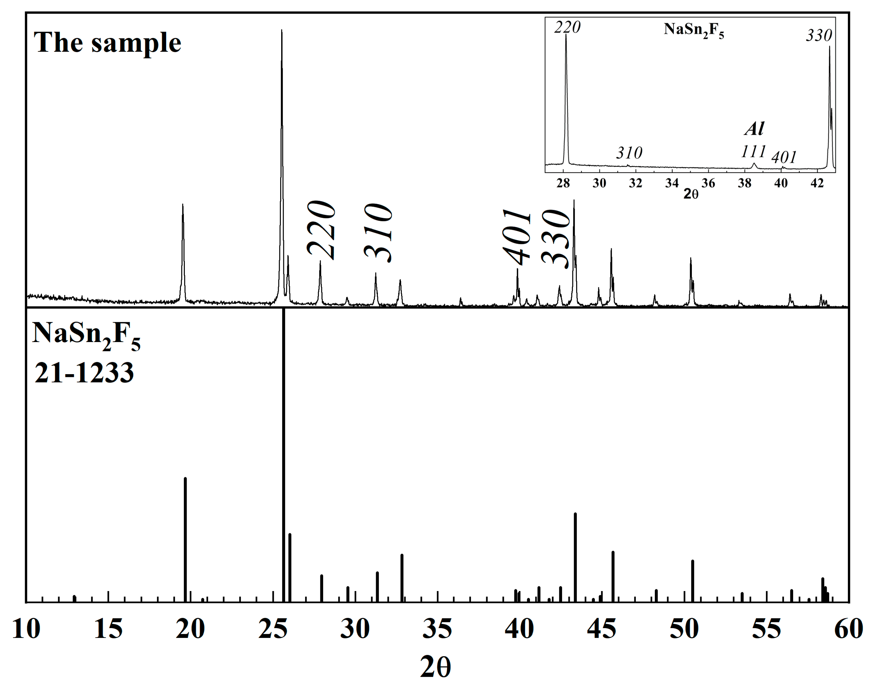
3.1.1. X-ray Diffraction Phase Analysis

The quality of synthesized crystals was determined using XRD. The resulting NaSn2F5 powder diffraction pattern is shown in Figure 1 along with a line diagram of the powder pattern corresponding to powder database card 21-1233 (NaSn2F5 P42/nbc, a = 9.020(3) Å, c = 13.686(3) Å, V = 1113.50 Å3) [28].
The quality of diffraction pattern indexing was determined using the difference between indexing parameters Q:
ΔQ = Qexp − Qcalc,
while the indexing parameter was determined using the formula:
Q = 10,000/d2,
where d is interplanar spacing, Å.
The results of powder diffraction pattern indexing are presented in Table 1.
The obtained cell parameters (Table 1) are in good agreement with the powder database data. Small deviations of the indexing parameters ΔQ indicate a good degree of crystallization of the sample. There are no foreign impurities according to XRD data.
To determine the crystals’ faceting, they were deposited on a polished aluminum substrate. The crystals were distributed via vibration over the surface of the substrate in such a way that they formed a uniform coating in one layer. The crystals were located independently of each other and were fixed with an X-ray amorphous film. A sample weighing approximately ~3 mg was distributed over ~1 cm2 of the substrate surface area where the X-ray beam hit. When recording the diffraction pattern, a classic pattern for a textured sample was observed (Figure 1 inset). This is mainly represented by reflections of the (hh0) type, which indicate the formation of a prismatic crystal habit by the (110) face.

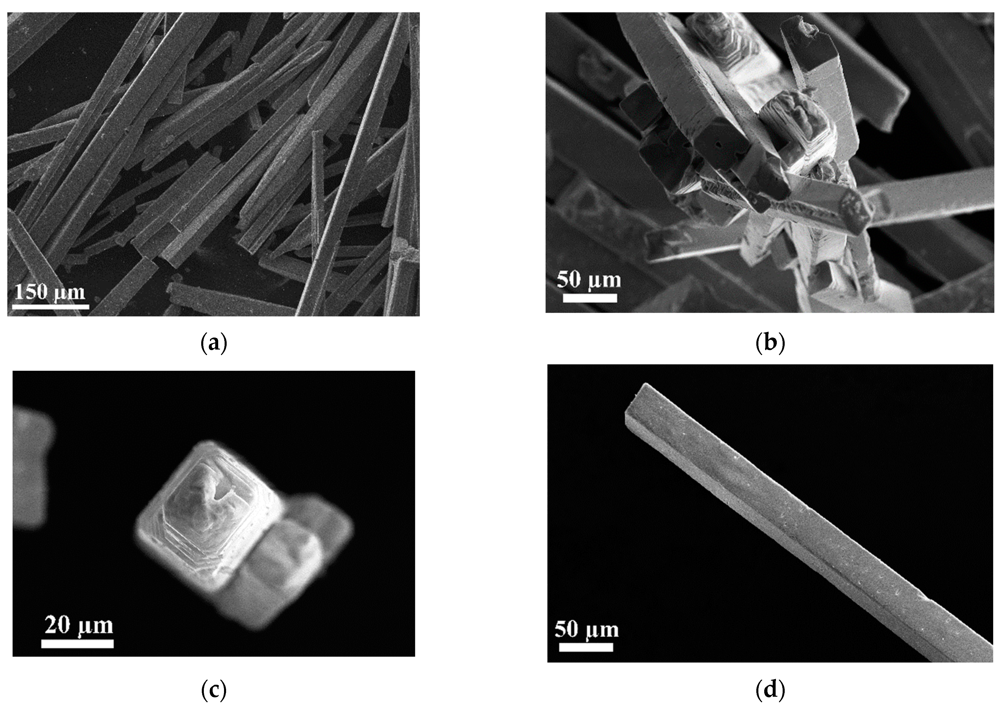
3.1.2. Scanning Electron Microscopy

The results of the SEM investigation of NaSn2F5 crystals are presented in Figure 2.
NaSn2F5 crystals are transparent and have a long prismatic shape. On the electron micrographs, one can see quadrangular prisms with a height of 300 to 1500 μm (Figure 2a). The cross section of the prisms is represented either by squares, which is consistent with a tetragonal structure (P42/nbc, point group 4/mmm), or by rectangles with an aspect ratio of 1.2–1.5 (Figure 2b,c). As a result of spontaneous crystallization from the solution, imperfect crystals are obtained. The side walls are rough, apparently etched with a solution in some places (Figure 2d). Some of the crystals were broken during the process of drying and placing on a stage for microscopic investigation.
Macroscopically, the NaSn2F5 faces are atomically smooth with kinks only in the region of steps, corresponding to tangential (layer-by-layer) crystal growth. Figure 2c shows growth steps perpendicular to the [001] direction of the tetragonal structure. The upper steps are represented by octagons, the sides of which are perpendicular to the directions [010], [100], [110], and [1 1 ¯ 0]. At the top of the crystal, there is a vicinal growth hillock where growth has been interrupted. The crystal is faceted by the planes of the (110) and (100) sets. The (100) faceting planes are practically degenerate. The observation of several crystal cleavages indicates that defect-free prisms grow with a square cross section; in the presence of a defect in the cross section, the crystals have a rectangular cross section.
Features of the crystals’ faceting are associated with the formation of the (110) plane. Consideration of the crystal structure shows that this plane can be formed by a plane of tin atoms or a plane containing sodium and tin atoms. In the first case, the surface is formed by chains of fluorine atoms parallel to the crystallographic axis c; they are interspersed with wide bands containing non-bonding (filled) orbitals of tin atoms. The orbitals lie in the plane of atoms. In the second case, chains of sodium atoms are located between chains of tin atoms, between which there are fluorine atoms. The non-bonding orbital is located perpendicular to the plane. In both cases, the attachment of atoms to a given face is complicated by the presence of a large area occupied by non-bonding tin orbitals.
In solutions, tin cations mainly form [SnF3] ions, as was shown earlier in [30]. At the same time, a small number of [Sn2F5] ions are present in the solution. They only participate in the NaSn2F5 crystal formation. When considering the structure (NaSn2F5 P42/nbc a = 9.02 Å, c = 13.685 Å [28]), fragments of [SnF2-F-SnF2] can be distinguished, and the distance between the fluorine and tin atoms is 2.07–2.09 Å. The bridging fluorine atom is 2.22 Å away from both tin atoms. The angle between the nearest fluorine atoms is 89°. They have angles of 81–84° with a bridging fluorine atom. The angle of the bridging fluorine atom Sn-F-Sn is 134°. Pairs of fluorine atoms relative to the Sn–F–Sn chain are in the trans position. This is also true for non-bonding orbitals of tin atoms. The NaSn2F5 crystal growth process probably proceeds as follows. The [Sn2F5] ion approaches the (001) face of the growing crystal almost perpendicularly. In this case, the ion forms two Sn–F bonds which are 2.53 Å long. One bond is formed from fluorine atoms of the crystal to the nearest tin atom of the [Sn2F5] ion. The second bond is formed from the fluorine atom of the [Sn2F5] ion to the tin atom of the crystal. These two bonds fix the [Sn2F5] ion on the (001) face of the growing crystal. At this time, a tin atom of the surface and a tin atom of the ion involved in the bond formation complete their polyhedron to four fluorine atoms. These fluorine atoms form a disphenoid due to their repulsion from the non-bonding orbital of the tin atom. The tin atoms participating in the addition of the [Sn2F5] ion turn their non-bonding orbitals to the trans position relative to the formed bonds. Sodium cations fill the channels of fluorine atoms which form in the structure after the addition of [Sn2F5] ions to the (001) face. The described mechanism explains the formation of long prismatic crystals with a large aspect ratio, the value of which can exceed 1000.
Usually, the sizes of crystals grown via spontaneous crystallization from supersaturated solutions are related to the cell parameter as follows: the smaller the cell parameter, the larger the crystal size is in the direction of this parameter. In our case, the crystal grows in the direction of the largest parameter c (~13.7 Å), but the symmetry axis 42, which coincides with this direction, is helical. Thus, it is possible to conditionally reduce the effective size of the parameter c by a factor of 2, which makes it smaller than the parameter a (~9 Å) and corresponds to the usual behavior of a crystal during growth.
On the energy dispersive X-ray spectrum of the sample (Figure 2e), only Na, Sn and F can be seen. The carbon C peaks are associated with the use of an electrically conductive carbon substrate in the SEM study. The atomic amounts of the elements are Na 11.17%, Sn 22.81%, F 53.23%, and C 12.79%.
The synthesized crystals were used to obtain a nanocomposite for incorporation into the channels of SWCNTs.

3.2. Investigation of the NaSn2F5@SWCNT Nanocomposite

3.2.1. Transmission Electron Microscopy and Structure Modelling

Figure 3a shows a 22.4 nm-wide bundle of carbon nanotubes with diameters from 1.5 to 2.2 nm, continuously filled with NaSn2F5. An enlarged fragment with a clear structural motif was chosen to model the structure (Figure 3b). In the micrograph, the greatest contrast is provided by tin atoms (ZSn = 50, black balls in Figure 3b) forming hexagons. The presence of sodium atoms (ZNa = 11) leads to some blurring of the cationic motif. Fluorine atoms have a low atomic number (ZF = 9) and are not observed in the micrograph. Carbon atoms (ZC = 6) merge in the area of the rounded walls of carbon nanotubes, where they overlap and form visible boundaries. The SWCNT diameter measured from the TEM image is dt~1.55 nm, and the sizes of the hexagons of tin atoms are a~0.87 nm and b~0.69 nm (Figure 3b).
The development of nanocomposite atomic models is based on the bulk crystal structure, interatomic distances and the stoichiometry of substances incorporated into SWCNT channels.
Based on the results of TEM analysis (Figure 3a,b), a chiral SWCNT (16,6) with a calculated diameter of 1.54 nm was selected to model the structure. The NaSn2F5 fragment was obtained from the structure of NaSn2F5 (P42/nbc a = 9.02 Å, c = 13.685 Å [28]). The selected fragment corresponds to the projection onto the (110) plane of the original structure. The axis of the nanotube coincides with the direction [2 2 ¯ 3] of the sodium pentafluorodistannate’s tetragonal structure. Combining the calculated SWCNT fragment and NaSn2F5 fragment, we obtained an atomic model of the NaSn2F5@SWCNT nanocomposite (Figure 3c). The crystal model is represented by 90 cations (30 Na atoms and 60 Sn atoms) and 150 anions (F atoms). The SWCNT model is represented by 1208 carbon atoms. The diameter of the modelled SWCNT is dtm~1.54 nm, and the sizes of the hexagons of tin atoms are am~0.88 nm and bm~0.68 nm (Figure 3c). The sizes obtained from the model are in good agreement with the actual sizes measured from the microphotograph.
Verification of the constructed structural model is carried out through the modeling of a TEM image and its comparison with the original micrograph. The simulation conditions are as follows: accelerating voltage 200 kV, spherical aberration 1.2. The resulting TEM model (Figure 3d) corresponds to the micrographs obtained experimentally (Figure 3b).
Figure 4a shows a unit cell of NaSn2F5 (P42/nbc a = 9.02 Å, c = 13.685 Å [28]) projected onto the (001) plane. The (110) plane represented by tin atoms located on the diagonal of the cell base is clearly visible (Layer №1). On both sides of it, two planes of tin atoms are parallel, one of which is Layer №2. The fluorine atoms (green balls) bound to tin atoms in the two layers form channels in which sodium atoms are located (orange balls). In the fragment highlighted with black lines (Figure 4a), corresponding to the SWCNT channel, the stoichiometric composition of the compound is completely preserved. Figure 4b shows a fragment of the NaSn2F5 structure, which is located in the nanotube channel (Figure 3c) in its projection onto the (001) plane. The nanotube axis is horizontal.
3]. Tin layer №1 is shown as a blue grid and tin layer №2 is shown as a sky-blue grid.
Figure 4c shows a fragment of the NaSn2F5 structure in its projection onto the (110) plane. It contains only two layers of tin atoms (Layer №1, №2) and stoichiometrically related fluorine and sodium atoms. The black lines indicate the boundaries of the fragment included in the SWCNT (16,6) channel. The direction coinciding with these lines corresponds to the crystallographic direction [2 2 ¯   3] of the NaSn2F5 structure. The NaSn2F5 fragment introduced into the SWCNT is represented by two planes of Sn cations (blue atoms—layer №1; sky blue atoms—layer №2), which provide contrast in high-resolution electron microscopy (EM) images. The first layer of Sn cations forms a hexagonal grid with Sn atoms located at the nodes (the grid shown in blue in Figure 4c). The second layer of tin atoms is less dense, and they are arranged according to the law of the closest spherical packing in a plane, but with a distance between atoms that is twice as large as in layer №1 (the grid shown in sky blue in Figure 4c). The hexagons of the first layer are located parallel to the nanotube axis, and atoms of the second layer are located above the centers of the first layer hexagons.
The resulting structural model and EM image of NaSn2F5@SWCNT are consistent with the sizes and contrast of the HRTEM image.

3.2.2. Raman Spectroscopy

The most interesting characteristic features of carbon nanotubes’ Raman spectra are:
  • RBM-mode, or first-order mode (radial breathing mode, ~100–350 cm−1), corresponds to radial vibrations of carbon atoms. It is a unique phonon mode, appearing only in carbon nanotubes. It is possible to estimate the diameter distribution of SWCNTs from the positions of the RBM peaks.
  • G-mode (tangential C-C stretch mode, ~1550–1600 cm−1) characterizes the sp2 vibrational mode. Unlike graphene/graphite (G~1580 cm−1), the G band of carbon nanotubes consists of several peaks due to twisting effects. The two main components are G+ (oscillations of atoms parallel to the nanotube axis—LO phonon mode) and G- (oscillations of atoms in the direction perpendicular to the axis of the nanotube tangentially to its wall—TO phonon mode) [31,32,33].
Table 2 shows the RBM band frequencies and SWCNT diameters calculated from the equation:
ωRBM = A/dt + B,
where A = 234 cm−1 nm and B = 10 cm−1 nm [31].
The diameters of nanotubes obtained from the analysis of the RBM peaks of Raman spectra, in particular 1.54 nm (Table 2), in the composition of the nanocomposite is in agreement with the SWCNT (16,6) chosen earlier for modeling the atomic structure of NaSn2F5@SWCNT.
According to the Kataura plot, at such diameters of nanotubes (Table 2) and at laser energies of ~2.33 eV and ~1.96 eV, SWCNTs of a semiconducting type are mostly excited [34].
Figure 5 shows the G regions of Raman spectra of unfilled carbon nanotubes and the NaSn2F5@SWCNT nanocomposite and the results of their fitting.
The G band in nanotubes contains several modes with different symmetries. The tangential modes that are Raman-active exhibit A1g, E1g and E2g symmetries, which can be established only using polarization studies [35]. In our case, fitting was carried out using two peaks with PseudoVoight lineshape (Figure 5c–f). The change in the positions of the G+ and G− peaks after SWCNT filling (Table 3) can indicate a shift in electron density (Figure 5a,b).
When using a green laser, an upshift in the G+ mode and a downshift in the G− mode are observed after filling the SWCNT channels (Table 3). In addition, a change in the G peak shape is observed in the case of NaSn2F5@SWCNT nanocomposite due to broadening, downshift and an increase in the intensity of the G− component. This is probably due to an increase in the contribution of metallic nanotubes, which are smaller in number but present in the sample, to the spectrum. When irradiated with a red laser, a stronger G+ mode upshift (approximately seven times greater than that when using a green laser) and a G− mode upshift by 13.8 cm−1 are observed (Table 3). Such upshifts clearly indicate a shift in electron density from the nanotube walls to the incorporated NaSn2F5 crystals, which characterizes the compound as an electron acceptor. Based on the structural model, fluorine atoms directly come into contact with nanotube walls. In this complex fluoride, it is difficult to guess how exactly this compound behaves with respect to the SWCNT walls. The electron density on tin atoms can probably be redistributed through the interaction of fluorine anions with the nanotube shell, which leads to its shift from the SWCNT walls to the intercalated compound.

4. Conclusions

In the investigation of crystal shape, the data obtained from electron microscopy and X-ray phase analysis made it possible to determine the morphology of NaSn2F5 crystals obtained from a saturated aqueous solution. The crystals have a long prismatic shape with an aspect ratio of length to width of about 1:100 and more. The NaSn2F5 compound has a tetragonal structure with the space group P42/nbc and the unit cell parameters a = 9.02 Å and c = 13.685 Å. The faceting of the prism is represented by the (110) face, while the (100) face degenerates. The faceting of the crystal is represented by the plane of the sodium pentafluorodistannate structure, which contains the maximum density of non-bonding orbitals of tin cations. The crystal grows due to the addition of [Sn2F5] ions, although their concentration in the solution is low and the main ion in the solution is the [SnF3] ion. At the ends of the prism, there are vicinal growth hillocks, on which there is a set of faces, namely (110) and (100). The crystal chemical analysis of the structure made it possible to suggest the growth mechanism of NaSn2F5. Growth occurs due to the addition of [Sn2F5] ions onto the (001) crystal face, which is unfolded by one tin atom on the (001) crystal surface. The ion joins it with the formation of two Sn–F bonds located perpendicular to the surface. Fluorine atoms complete the polyhedra of tin atoms at the crystal–ion interface, forming a disphenoid. Non-bonding orbitals with respect to the formed bond turn into the trans position. After that, sodium cations are incorporated into the structure.
A nanocomposite for incorporation, NaSn2F5@SWCNT, was synthesized from the melt using the capillary wetting technique. It was possible to determine the structural model of the incorporated crystal. In the EM images, one can observe a pattern resembling the closest spherical packing. Crystal chemical analysis of the NaSn2F5 structure showed that tin cations in planes perpendicular to the [110] direction occupy positions of the closest spherical packing, but with increased distances between atoms (by approximately two times for the first type of tin cation plane and approximately four times for the second type). The superposition of these two planes of the structural model explains the image obtained with the electron microscope. The model is represented by a fragment of the NaSn2F5 structure projected onto the (110) crystallographic plane, which is the face of the prism of bulk NaSn2F5 crystals. The nanotube axis corresponds to the direction [2 2 ¯ 3] of the sodium pentafluorodistannate tetragonal structure. The incorporated fragment is represented by two planes of tin cations. The first layer of cations forms a hexagonal network with Sn atoms located at its nodes. Such a network can be considered as a closely packed spherical layer, in which a third of the atoms are missing. The second layer of tin atoms is less dense, and they are located according to the law of closest spherical packing in a plane, but with a distance between atoms two times greater than that in the first layer. These layers are present in the NaSn2F5 bulk structure, which cannot be described by a spherical packing in the classic form. The constructed atomic model was verified by modeling the EM image, which is in agreement with the real HRTEM picture. The dimensions of the model are consistent with the experimental data. The SWCNT diameter of 1.54 nm, revealed by the results of Raman spectroscopy performed on the nanocomposite, coincides with the modelled nanotube (16,6) diameter. The shift in the G bands of the nanocomposite Raman spectra compared to empty SWCNTs at excitation wavelengths of 532 nm and 633 nm indicates a shift in electron density from the nanotube walls to the embedded 1D NaSn2F5 crystals.
This nanocomposite was obtained for the first time. It is possible to use it in the creation of additives for fluoride-ion galvanic cells, as a working element for the determination of fluorine, etc.

Author Contributions

Conceptualization, R.M.Z.; investigation, R.M.Z., E.A.L. and A.S.K.; writing—original draft preparation, R.M.Z., E.A.L. and A.S.K.; writing—review and editing, R.M.Z. and E.A.L.; visualization, E.A.L. All authors have read and agreed to the published version of the manuscript.

Funding

This work was performed within the state assignment of Federal Scientific Research Center “Crystallography and Photonics” of the Russian Academy of Sciences.

Data Availability Statement

Not applicable.

Acknowledgments

This work was performed within the State Assignment Federal Scientific Research Centre “Crystallography and Photonics” of the Russian Academy of Sciences and was performed using the equipment of the Shared Research Centre of the FSRC “Crystallography and Photonics” of RAS.

Conflicts of Interest

The authors declare no conflict of interest.

References

  1. Monthioux, M. Carbon Meta-Nanotubes: Synthesis, Properties and Applications; Wiley: Hoboken, NJ, USA, 2012. [Google Scholar]
  2. Endo, M.; Strano, M.S.; Ajayan, P.M. Potential applications of carbon nanotubes. In Carbon Nanotubes: Advanced Topics in the Synthesis, Structure, Properties and Applications; Jorio, A., Dresselhaus, G., Dresselhaus, M.S., Eds.; Springer: Berlin/Heidelberg, Germany, 2008; pp. 13–62. [Google Scholar] [CrossRef]
  3. Kharlamova, M.V.; Kramberger, C. Applications of filled single-walled carbon nanotubes: Progress, challenges, and perspectives. Nanomaterials 2021, 11, 2863. [Google Scholar] [CrossRef] [PubMed]
  4. Yoon, J.; Kim, U.; Yoo, Y.; Byeon, J.; Lee, S.-K.; Nam, J.-S.; Kim, K.; Zhang, Q.; Kauppinen, E.I.; Maruyama, S.; et al. Foldable Perovskite Solar Cells Using Carbon Nanotube-Embedded Ultrathin Polyimide Conductor. Adv. Sci. 2021, 8, 2004092. [Google Scholar] [CrossRef] [PubMed]
  5. Zhu, S.; Sheng, J.; Chen, Y.; Ni, J.; Li, Y. Carbon nanotubes for flexible batteries: Recent progress and future perspective. Natl. Sci. Rev. 2021, 8, nwaa261. [Google Scholar] [CrossRef] [PubMed]
  6. Halankar, K.K.; Mandal, B.P.; Tyagi, A.K. Superior electrochemical performance of MoS2 decorated on functionalized carbon nanotubes as anode material for sodium ion battery. Carbon Trends 2021, 5, 100103. [Google Scholar] [CrossRef]
  7. Duong, H.M.; Tran, T.Q.; Kopp, R.; Myint, S.M.; Peng, L. Chapter 1—Direct spinning of horizontally aligned carbon nanotube fibers and films from the floating catalyst method. In Nanotube Superfiber Materials (Second Edition); Schulz, M.J., Shanov, V., Yin, Z., Cahay, M., Eds.; William Andrew Publishing: Norwich, NY, USA, 2019; pp. 3–29. [Google Scholar]
  8. Duong, H.M.; Myint, S.M.; Tran, T.Q.; Le, D.K. Chapter 6—Post-spinning treatments to carbon nanotube fibers. In Carbon Nanotube Fibers and Yarns; Miao, M., Ed.; Woodhead Publishing: Sawston, UK, 2020; pp. 103–134. [Google Scholar]
  9. Kamedulski, P.; Lukaszewicz, J.P.; Witczak, L.; Szroeder, P.; Ziolkowski, P. The importance of structural factors for the electrochemical performance of graphene/carbon nanotube/melamine powders towards the catalytic activity of oxygen reduction reaction. Materials 2021, 14, 2448. [Google Scholar] [CrossRef]
  10. Hu, Z.; Breeze, B.; Kashtiban, R.; Sloan, J.; Lloyd-Hughes, J. Zigzag HgTe nanowires modify the electron–phonon interaction in chirality-refined single-walled carbon nanotubes. ACS Nano 2022, 16, 6789–6800. [Google Scholar] [CrossRef]
  11. Faulques, E.; Kalashnyk, N.; Slade, C.A.; Sanchez, A.M.; Sloan, J.; Ivanov, V.G. Vibrational and electronic structures of tin selenide nanowires confined inside carbon nanotubes. Synth. Met. 2022, 284, 116968. [Google Scholar] [CrossRef]
  12. Vorfolomeeva, A.A.; Pushkarevsky, N.A.; Koroteev, V.O.; Surovtsev, N.V.; Chuvilin, A.L.; Shlyakhova, E.V.; Plyusnin, P.E.; Makarova, A.A.; Okotrub, A.V.; Bulusheva, L.G. Doping of carbon nanotubes with encapsulated phosphorus chains. Inorg. Chem. 2022, 61, 9605–9614. [Google Scholar] [CrossRef]
  13. Cao, K.; Biskupek, J.; Stoppiello, C.T.; McSweeney, R.L.; Chamberlain, T.W.; Liu, Z.; Suenaga, K.; Skowron, S.T.; Besley, E.; Khlobystov, A.N.; et al. Atomic mechanism of metal crystal nucleus formation in a single-walled carbon nanotube. Nat. Chem. 2020, 12, 921–928. [Google Scholar] [CrossRef]
  14. Fan, X.; Dickey, E.C.; Eklund, P.C.; Williams, K.A.; Grigorian, L.; Buczko, R.; Pantelides, S.T.; Pennycook, S.J. Atomic arrangement of iodine atoms inside single-walled carbon nanotubes. Phys. Rev. Lett. 2000, 84, 4621–4624. [Google Scholar] [CrossRef]
  15. Fujimori, T.; Morelos-Gómez, A.; Zhu, Z.; Muramatsu, H.; Futamura, R.; Urita, K.; Terrones, M.; Hayashi, T.; Endo, M.; Young Hong, S.; et al. Conducting linear chains of sulphur inside carbon nanotubes. Nat. Commun. 2013, 4, 2162. [Google Scholar] [CrossRef] [PubMed] [Green Version]
  16. Lusk, M.T.; Hamm, N. Ab initio study of toroidal carbon nanotubes with encapsulated atomic metal loops. Phys. Rev. B 2007, 76, 125422. [Google Scholar] [CrossRef] [Green Version]
  17. Medeiros, P.V.C.; Marks, S.; Wynn, J.M.; Vasylenko, A.; Ramasse, Q.M.; Quigley, D.; Sloan, J.; Morris, A.J. Single-atom scale structural selectivity in Te nanowires encapsulated inside ultranarrow single-walled carbon nanotubes. ACS Nano 2017, 11, 6178–6185. [Google Scholar] [CrossRef] [PubMed] [Green Version]
  18. Sloan, J.; Kirkland, A.I.; Hutchison, J.L.; Green, M.L.H. Integral atomic layer architectures of 1D crystals inserted into single walled carbon nanotubes. Chem. Commun. 2002, 13, 1319–1332. [Google Scholar] [CrossRef]
  19. Anuchin, N.M.; Enyashin, A.N. Electronic and mechanical properties of endohedral composites of carbon nanotubes with potassium iodide: DFT study. J. Struct. Chem. 2023, 64, 662–673. [Google Scholar] [CrossRef]
  20. Eliseev, A.A.; Falaleev, N.S.; Verbitskiy, N.I.; Volykhov, A.A.; Yashina, L.V.; Kumskov, A.S.; Zhigalina, V.G.; Vasiliev, A.L.; Lukashin, A.V.; Sloan, J.; et al. Size-dependent structure relations between nanotubes and encapsulated nanocrystals. Nano Lett. 2017, 17, 805–810. [Google Scholar] [CrossRef]
  21. Kashtiban, R.J.; Patrick, C.E.; Ramasse, Q.; Walton, R.I.; Sloan, J. Picoperovskites: The smallest conceivable isolated halide perovskite structures formed within carbon nanotubes. Adv. Mater. 2023, 35, 2208575. [Google Scholar] [CrossRef]
  22. Zakalyukin, R.M.; Levkevich, E.A.; Kumskov, A.S.; Orekhov, A.S. Superionic conductor PbSnF4 in the inner channel of SWNT. AIP Conf. Proc. 2018, 1957, 030001. [Google Scholar] [CrossRef]
  23. Zakalyukin, R.M.; Levkevich, E.A.; Kumskov, A.S. Nanocomposite E(PbSnF4;SnF2)@SWCNT—Promising material for fluoride-ion batteries. Ceram. Int. 2022, 48, 26565–26574. [Google Scholar] [CrossRef]
  24. Zakalyukin, R.M.; Mavrin, B.N.; Dem’yanets, L.N.; Kiselev, N.A. Synthesis and characterization of single-walled carbon nanotubes filled with the superionic material SnF2. Carbon 2008, 46, 1574–1578. [Google Scholar] [CrossRef]
  25. Zakalyukin, R.M.; Demyanets, L.; Kiselev, N.; Kumskov, A.S.; Kislov, M.; Krestinin, A.; Hutchison, J. One-dimensional SnF2 single crystals in the inner channels of single-wall carbon nanotubes: I. Preparation and basic characterization. Crystallogr. Rep. 2010, 55, 507–512. [Google Scholar] [CrossRef]
  26. Zakalyukin, R.M.; Demyanets, L.; Kiselev, N. One-Dimensional SnF2 single crystals in the inner channels of single-wall carbon nanotubes: II. Structure and nanocomposite construction modeling. Crystallogr. Rep. 2010, 55, 688–694. [Google Scholar] [CrossRef]
  27. Donaldson, J.D.; O’Donoghue, J.D. Complex tin(II) fluorides. J. Chem. Soc. 1964, 44, 271–275. [Google Scholar] [CrossRef]
  28. McDonald, R.; Larson, A.; Cromer, D.T. The crystal structure of sodium pentafluorodistannate (II), NaSn2F5. Acta Crystallogr. 1964, 17, 1104–1108. [Google Scholar] [CrossRef]
  29. Zakalyukin, R.M.; Levkevich, E.A.; Nikolaeva, A.V. Synthesis and X-ray-graphical characteristics of the MeSn2F5 (Me = Na, K, Rb, Cs) fluoride-ion conductors. Fine Chem. Technol. 2021, 16, 426–437. [Google Scholar] [CrossRef]
  30. Birchall, T.; Dénès, G. A 19F, 119Sn nuclear magnetic resonance and 119Sn Mössbauer study of the SnF2–MF–H2O system. Can. J. Chem. 1984, 62, 591–595. [Google Scholar] [CrossRef]
  31. Dresselhaus, M.; Dresselhaus, G.; Saito, R.; Jorio, A. Raman spectroscopy of carbon nanotubes. Phys. Rep. 2005, 409, 47–99. [Google Scholar] [CrossRef]
  32. Dresselhaus, M.S.; Eklund, P.C. Phonons in carbon nanotubes. Adv. Phys. 2000, 49, 705–814. [Google Scholar] [CrossRef]
  33. Li, Z.; Deng, L.; Kinloch, I.A.; Young, R.J. Raman spectroscopy of carbon materials and their composites: Graphene, nanotubes and fibres. Prog. Mater. Sci. 2023, 135, 101089. [Google Scholar] [CrossRef]
  34. Kataura, H.; Kumazawa, Y.; Kojima, N.; Maniwa, Y.; Umezu, I.; Masubuchi, S.; Kazama, S.; Zhao, X.; Ando, Y.; Ohtsuka, Y.; et al. Optical absorption and resonance Raman scattering of carbon nanotubes. AIP Conf. Proc. 1999, 486, 328–332. [Google Scholar] [CrossRef]
  35. Jorio, A.; Dresselhaus, G.; Dresselhaus, M.S.; Souza, M.; Dantas, M.S.S.; Pimenta, M.A.; Rao, A.M.; Saito, R.; Liu, C.; Cheng, H.M. Polarized Raman study of single-wall semiconducting carbon nanotubes. Phys. Rev. Lett. 2000, 85, 2617–2620. [Google Scholar] [CrossRef] [PubMed]
Figure 1. X-ray powder diffraction pattern of NaSn2F5 crystals and line diagram from the 21-1233 powder database card. Inset: Texture diffraction pattern of a prismatic crystal’s face.
Crystals 13 01065 g001
Figure 2. SEM investigation of NaSn2F5 crystals: (a) accelerating voltage 15 kV, secondary electron detecting mode; (bd) accelerating voltage 20 kV, secondary electron detecting mode; (e) EDX spectrum.
Crystals 13 01065 g002aCrystals 13 01065 g002b
Figure 3. NaSn2F5@SWCNT TEM investigation and modelling. (a) SWCNT bundle filled with NaSn2F5. (b) Enlarged fragment of the filled SWCNT. (c) NaSn2F5@SWCNT nanocomposite structure model in a projection on the (110) plane of the tetragonal NaSn2F5 structure (Sn atoms are blue, Na atoms are orange, fluorine atoms are green, carbon atoms are grey). (d) NaSn2F5@SWCNT nanocomposite TEM image model.
Crystals 13 01065 g003aCrystals 13 01065 g003b
Figure 4. NaSn2F5 structure (Sn atoms are blue and sky blue, Na atoms are orange, fluorine atoms are green). (a) NaSn2F5 unit cell with two Sn (110) layers. The black lines highlight the volume of the structure, which includes the stoichiometric number of the compound atoms. (b) Structure fragment containing two tin layers, which is incorporated into the channel of SWCNT. Sn layer №1 is highlighted with a blue color, while Sn layer №2 is highlighted with a sky-blue color. (c) Projection of two layers of tin atoms onto the (110) plane. The black lines highlight the fragment that enters the SWCNT channel, coinciding with the direction [2 2 ¯ . Tin layer №1 is shown as a blue grid and tin layer №2 is shown as a sky-blue grid.
Crystals 13 01065 g004
Figure 5. Raman spectra of carbon nanotubes and NaSn2F5@SWCNT. (a) Shift of G modes obtained at 532 nm. (b) Shift of G modes obtained at 633 nm. (c,d) SWCNT G mode fitting. (e,f) NaSn2F5@SWCNT G mode fitting.
Crystals 13 01065 g005aCrystals 13 01065 g005b
Table 1. Indexing results.
d, ÅQexpI/Imaxh k lQcalcΔQ
119.5934.5272487.91332 0 0490.03−2.12
220.5824.3118537.8842 0 1543.22−5.34
325.5323.4860822.901002 1 2825.31−2.41
425.9183.4349847.56140 0 4851.10−3.54
527.8673.1990977.17152 2 0980.05−2.88
629.5123.02431093.3352 1 31091.282.05
731.2642.85871223.67123 1 01225.07−1.40
832.7412.73301338.82152 0 41341.13−2.31
939.6722.27011940.4852 1 51942.38−1.90
1039.8692.25931959.0834 0 01960.11−1.03
1140.4222.22972011.4424 0 12013.30−1.86
1241.0852.19522075.1673 1 42076.17−1.01
1342.4052.12992204.3683 3 02205.12−0.77
1443.3112.08742295.03514 1 22295.39−0.36
1544.8362.01992450.9844 2 02450.130.85
1645.5791.98872528.49252 1 62527.510.98
1748.2131.88602811.3664 0 42811.210.15
1850.4271.80823058.49233 3 43056.222.27
1953.4261.71363405.5030 0 83404.411.09
2056.4431.62893768.8745 2 23765.473.40
NaSn2F5 P42/nbc, a = 9.03(5) Å, c = 13.71(1) Å, V = 1119.2(4) Å3.
Table 2. RBM bands and SWCNT diameters.
LaserSWCNTNaSn2F5@SWCNT
RBM, cm−1dt, nmRBM, cm−1dt, nm
532 nm
(2.33 eV)
118.482.16136.951.84
136.891.84166.291.50
149.281.68203.561.21
168.191.48241.741.01
633 nm
(1.96 eV)
116.552.20116.322.20
131.601.92134.101.89
145.031.73161.641.54
Table 3. G-bands’ shift.
LaserG ModeSWCNTNaSn2F5@SWCNTΔG, cm−1
532 nm
(2.33 eV)
G+, cm−11579.171581.43+2.26
G−, cm−11557.861553.67−4.19
633 nm
(1.96 eV)
G+, cm−11572.941589.56+16.62
G−, cm−11550.061563.86+13.80
Disclaimer/Publisher’s Note: The statements, opinions and data contained in all publications are solely those of the individual author(s) and contributor(s) and not of MDPI and/or the editor(s). MDPI and/or the editor(s) disclaim responsibility for any injury to people or property resulting from any ideas, methods, instructions or products referred to in the content.

