Article

Growth and Characterization of All-Inorganic Halide Perovskite CsPbF3 Single Crystals

1
The Key Laboratory of Weak Light Nonlinear Photonics, School of Physics, Nankai University, Tianjin 300071, China
2
The State Key Laboratory of Intense Pulsed Radiation Simulation and Effect, Northwest Institute of Nuclear Technology, Xi’an 710024, China
3
Shenzhen Research Institute, Nankai University, Shenzhen 518083, China
*
Authors to whom correspondence should be addressed.
Crystals 2023, 13(5), 765; https://doi.org/10.3390/cryst13050765
Submission received: 4 April 2023 / Revised: 25 April 2023 / Accepted: 27 April 2023 / Published: 4 May 2023
(This article belongs to the Special Issue Photoelectric Functional Crystals)

Abstract

:
Lead-based halide perovskite semiconductors have demonstrated considerable potential in optoelectronic applications. However, the lack of high-quality crystals suitable for research has led to rare reports on CsPbF3 single crystals. Good quality CsPbF3 single crystals were successfully grown using the Bridgman method. The structure, luminescence, and electrical properties of crystals were investigated. At room temperature, the crystal structure was determined to be cubic perovskite, with a calculated bandgap of 3.68 eV. The measured emission spectrum showed one broad emission peak at approximately 400 nm. Three decay time constants were obtained from a sum of exponential functions fit to the fluorescence decay curve: 0.4 ns, 2.4 ns, and 15.0 ns for fast, middle, and slow decay times, respectively. The decay times excited by pulsed X-ray were measured to be 2.2 ns and 10.2 ns, indicating that CsPbF3 is an ultrafast scintillator. Furthermore, the electrical properties demonstrated that CsPbF3 exhibits high ion mobility, which is approximately 20 times that of electron mobility.

1. Introduction

Lead-based halide perovskites with a stoichiometric ratio of ABX3 (where A = MA+, GA+, and Cs+; B = Pb2+; X = Cl, Br, and I) exhibit high carrier mobility, long diffusion length, adjustable bandgap, and defect tolerance. Therefore, they are exceptional candidates for various applications such as photodetectors, radiation detectors, solar cells, light-emitting diodes, and other fields [1,2,3,4,5,6,7]. Compared with the organic-inorganic hybrid perovskites, all-inorganic perovskite CsPbX3 (X = Cl, Br, and I) is more appealing for radiation detection due to its superior stability, optoelectronic performances, and radiation hardness. CsPbI3 has garnered considerable attention due to its exceptional thermal stability and ideal bandgap of approximately 1.75 eV, making it an attractive candidate for tandem applications. Tan et al. showed a study on the thermal stability of low-dimensional perovskites that utilize hydrophobic organic ammonium salts and their potential to safeguard CsPbI3 through passivation. The highest-performing solar cell device employing CsPbI3 as its primary material demonstrated an unprecedented efficiency of 21.0% while sustaining high stability [8,9]. CsPbBr3 quantum dots emit light at a narrow band at room temperature, which makes them highly desirable for use in conventional light-emitting devices as well as emerging quantum light sources [10]. He et al. reported that all inorganic perovskite CsPbBr3 devices resolve 137Cs 662 keV γ-rays with 1.4% energy resolution, the CsPbBr3 detector exhibited an excellent hole mobility lifetime product of 8 × 10⁻³ cm2 V−1, and a long hole lifetime of up to 296 μs. This research has established perovskite CsPbBr3 semiconductors as exceptional candidates for high energy γ-ray detection in the new generation [11]. Although CsPbCl3 has received less attention than CsPbBr3, some researchers have reported its optical and photodetection properties. CsPbCl3 crystals have shown excellent ultrafast scintillation at low-temperature and semiconductor detection performance [12,13].
In particular, aluminium gallium nitride (AlxGa1−xN) is used to fabricate the visible-blind photodetector where the band gap energy can be adjusted from 3.4 eV (GaN) to 6.2 eV (AlN) by modifying the composition parameter x. Typically, the composition is altered to achieve a long wavelength cut-off below 300 nm by selecting a sufficiently high value for x. Conventional photodiodes and Schottky barrier detectors can be created, although the latter are somewhat simpler to manufacture. Silicon carbide (SiC) photodiodes are sensitive to light with wavelengths below approximately 355 nm, making them suitable for visible-blind detection. CsPbF3 perovskite semiconductors possess a relatively large band gap energy of approximately 3.68 eV and a direct band gap, resulting in a well-defined long wavelength cut-off. Compared to the difficulty of growing GaN and SiC crystals, CsPbF3 single crystals are easier to obtain in excellent quality, indicating their potential for application in visible-blind photodetectors. CsPbF3 is a direct bandgap semiconductor with optical activity, which can effectively be used in optical and optoelectronic devices [14]. Bouznik et al. investigated the fast conduction of fluoride ions in CsPbF3 polycrystals using continuous wave and pulse NMR techniques. The CsPbF3 crystals were grown from the melt in an Ar-HF mixture atmosphere using a high-frequency crystallization apparatus [15]. Berastegui et al. observed a transition of CsPbF3 from a rhombohedral distorted perovskite structure to a cubic perovskite structure at 187 K through neutron diffraction experiments, and the transition was found to be discontinuous [16]. In the low-temperature phase, cations exhibit a parallel displacement away from the center of their anion polyhedrons, which proves the existence of ferroelectric properties [17]. The CsPbF3 polycrystalline sample was prepared by mixing stoichiometric amounts of CsF and PbF2 in a dry box filled with nitrogen gas. Wang et al. circumvent the multiple bottlenecks of Li+ ion batteries by using CsPbF3 as a solid-state electrolyte. The battery cycled stably at 25 °C for 4581 h without considerable capacity fade [18]. Therefore, this ternary compound exhibits potential characteristics in terms of its performance. The optical performance of CsPbF3 has not been investigated and presented yet, mainly due to the difficulty in obtaining high-quality CsPbF3 crystals. Most perovskite devices are based on polycrystalline and thin films, which are greatly affected by a high density of traps and grain boundaries. In contrast, single crystals have significantly lower trap densities. However, there is insufficient research on the optical performance of CsPbF3 single crystals, and many blanks need to be filled. As a result, the potential application of polycrystalline devices is significantly limited.
In this study, good-quality CsPbF3 single crystals were grown by the Bridgman method. The optical and luminescence properties of the crystal were characterized and analyzed. The results demonstrate that CsPbF3 crystal exhibits ultrafast scintillation and has potential as an ultrafast scintillation crystal. Additionally, the electrical properties of the crystals were characterized, revealing that CsPbF3 single crystals exhibit high ion mobility and can be applied as a semiconductor.

2. Materials and Methods

2.1. Crystal Growth of CsPbF3

The Bridgman method involves using a furnace with a hot and cold zone to create a temperature gradient, where the hot zone is maintained at a temperature above the melting point of the crystal [19,20,21]. The melt moves from the hot zone to the cold zone to complete the crystallization of the material by controlling the descending system. This method is commonly used to prepare single crystals of alkali metal, alkaline earth metal halides, and fluorides. The CsPbF3 single crystals were prepared using the vertical Bridgman method. The advantages of preparing CsPbF3 single crystals by the Bridgeman method mainly include the following aspects. Firstly, the raw material is sealed in the crucible, which reduces the leakage and pollution caused by the volatilization of the raw material, so the composition of the crystal is easy to control. Secondly, the perovskite structure can easily accommodate impurity atoms, which is conducive to the removal of volatile impurities, thereby improving the crystal quality. The experimental configuration for crystal growth is depicted in Figure 1. High-purity powders of CsF (99.99%, Aladdin) and PbF2 (99.99%, Aladdin) were mixed in a 1:1 ratio and ground thoroughly. The raw materials were mixed and put into a platinum crucible. The crucible was then placed inside a sealed quartz crucible. The crucible was moved to the Bridgman furnace for the growth of single crystals. The furnace temperature was set to 30°C higher than the melting point of the growth crystal. After the raw material was melted and soaked for 24 h, the drop controller system started to work, and the growth rate was set to 0.5 mm/h. Subsequently, CsPbF3 single crystal growth was started, and the temperature gradient in the solid-liquid interface was about 20–30 °C/cm. After the entire solution was crystallized, the furnace was cooled down to room temperature at a rate of 50 °C/h. The crystal boules obtained were cut into plates, polished, and sealed.

2.2. Characterization

The crystal structure of CsPbF3 was analyzed using a Bruker D8 advanced X-ray powder diffractometer with Cu Ka radiation (λ = 1.5406 Å), scanning 2θ from 10–90° with a step size of 0.02°. The thermal stability was tested using a NETZSCH STA449F3 instrument under a nitrogen atmosphere, with a heating program from 20 °C to 800 °C at a heating rate of 10 °C/min. The cathodoluminescence (CL) spectroscopy was tested using a HORIBA i-CLUE spectrometer with an electron beam voltage of 30 keV. The transmission spectrum was measured using a Hitachi U-4100 UV-vis spectrophotometer. The photoluminescence (PL) spectrum and fluorescence decay curve were measured using the FS5 spectrometer from Edinburgh, UK. The X-ray excited luminescence (XEL) and decay kinetic curve excited by X-rays were characterized with the Dongyi DF-7000X X-ray spectrometer with a rhodium target X-ray tube operating at 40 kV. Electrical properties were measured using the Keysight B1500A semiconductor analyzer.

3. Results and Discussion

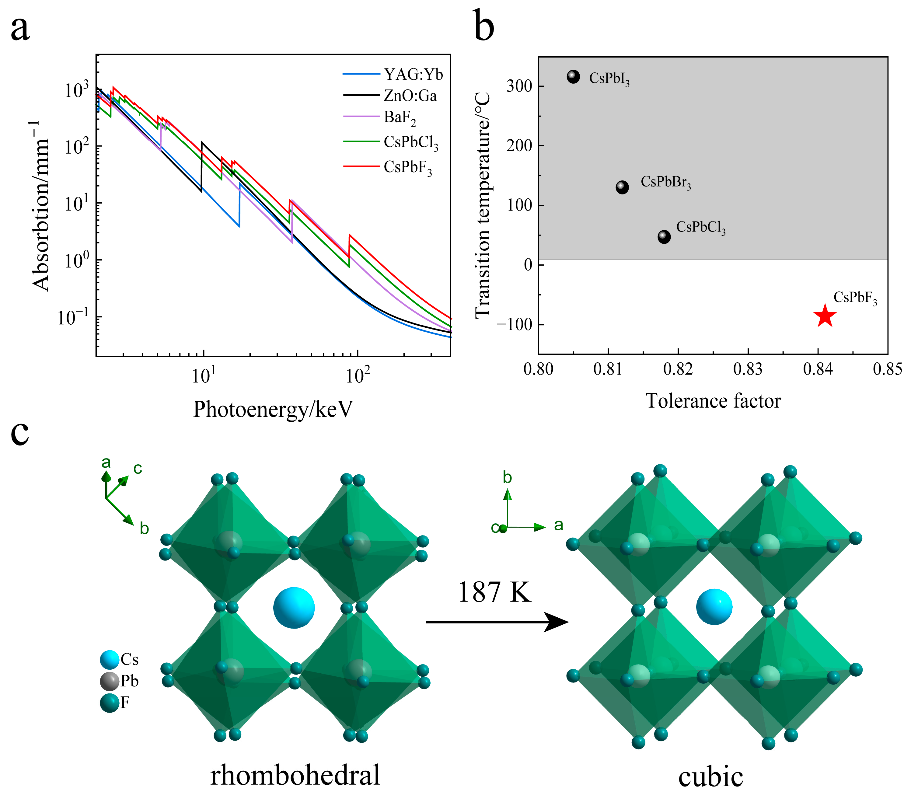
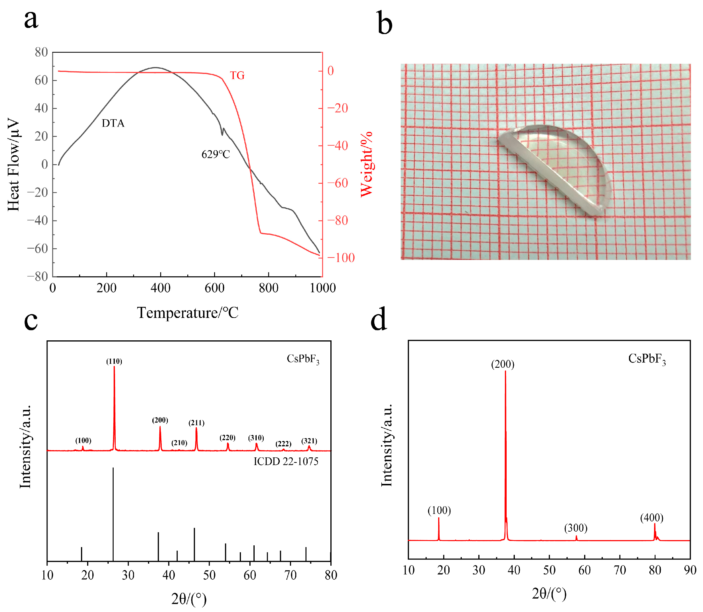
3.1. Crystal Structure and Growth

Figure 2a illustrates the linear attenuation coefficients as a function of photon energy for several fast scintillation crystals, which were calculated using the NIST XCOM photon cross-section database. The red line in Figure 2a depicts the linear attenuation coefficient of CsPbF3. It has been observed that the value of the red line is marginally higher than that of the other curves, indicating that a thinner layer of material is required to achieve effective photon cut-off. Compared with other ultrafast inorganic scintillators, CsPbF3 has superior photon cut-off capabilities due to its high average atomic number (Cs: 55, Pb: 82, and F: 9) and relatively high density (ρ = 5.6 g/cm3). The statement suggests that CsPbF3 is capable of absorbing X-rays more efficiently compared to other materials, indicating its potential superiority in X-ray imaging applications.
One of the key aspects is the stability of perovskite materials, which can affect the crystal structure transition, has not received sufficient attention. ABX3-type perovskites can form different crystal structures based on the sizes of the A, B, and X ions. The first requirement is the octahedral factor, which is calculated below:
μ = r B r X
where r B and r X are the efficient ionic radii of B and X, respectively. The octahedral factor is an important parameter for determining the stability of the ABX3-type perovskite structure. When the octahedral factor falls in the range of 0.4420–0.8950, the octahedral structure can remain relatively stable. The octahedral factor of CsPbF3 is 0.8947, which is close to the edge of the stable region. The most commonly used and most successful geometric ratio is the Goldschmidt tolerance factor ( t G ) [22,23], which can be expressed as follows:
t G = r A + r X 2 ( r B + r X )
where r A is the efficient ionic radii of A. The Goldschmidt tolerance factor is widely used to investigate distorted perovskites. A sTable 3D perovskite phase with high absorption coefficients can be formed within the range of 0.8–1.0. CsPbF3 has a tolerance factor of 0.841, which is close to the edge of the stable perovskite structure. This indicates that CsPbF3 may display unique properties because of its borderline stability.
Figure 2b illustrates the relationship between cubic transition temperature and Goldschmidt tolerance factor of CsPbX3 (X = F, Cl, Br, and I) crystals. CsPbI3 tends to crystalize into a yellow non-perovskite phase, which has poor optoelectronic properties at room temperature [24]. There are cubic phase transitions as CsPbCl3 and CsPbBr3 are cooled from high temperature to room temperature. The Bridgman method used to grow these crystals can result in residual stress, twinning, and cracking, which can reduce the yield of high-quality single crystals. Although Zhao et al. managed to find some good quality CsPbBr3 crystals that exhibit an energy resolution of 5.5%, the yield of high-quality single crystals was extremely low (less than 5%) [25]. However, CsPbF3 is in a cubic phase at room temperature, and its phase transition temperature is as low as 187 K. There is no cubic phase transition-induced defects as the crystal grows by the melting method. Due to the strong polar molecular bond of Cs+ and F, CsPbF3 is susceptible to being hygroscopic, and it is prone to oxidation and volatilization at high temperatures. Therefore, obtaining high-quality CsPbF3 crystals can be a challenging task. As shown in Figure 2c, the cubic CsPbF3 is formed by the lead cation and six fluorine ions surrounding the lead cation to form an octahedral coordination. The lead cation locates at the center of the fluorine octahedron; the caesium cation is in the cavity created by the octahedron. At around 187 K, there is the phase transition of CsPbF3 from the rhombohedral distorted perovskite structure to the cubic phase.
The differential thermal analysis (DTA) and thermogravimetric analysis (TG) curves of the perovskite powder are shown in Figure 3a. The DTA heating curve (black line) shows an evident endothermic peak at 629 °C; it is the absorption peak temperature that corresponds to the melting point of CsPbF3. The TG curve indicates that the crystal melts at 629 °C and experiences a steep weight loss, which suggests strong volatility at high temperatures. When using the Bridgman method to prepare crystals, the furnace temperature must be carefully controlled based on the melting point of the crystal. The furnace temperature should be set above the melting point but not excessively high when preparing crystals using the Bridgman method. This is because excessively high temperatures can cause the volatilization of raw materials and lead to component segregation during the crystal preparation process. Hence, the furnace temperature is typically maintained at approximately 660 °C. Figure 3b displays a high-quality CsPbF3 single crystal, which has been polished to a transparent finish with a thickness of 3 mm. The optical clarity of the crystal is apparent, as it is colorless and devoid of any visible macroscopic defects.
In Figure 3c, a comparison is presented between the XRD pattern of CsPbF3 and the standard PDF card (ICDD 22-1075) for CsPbF3. The analysis indicates that CsPbF3 has a cubic perovskite structure at room temperature. Additionally, when the crystal boule experiences an impact force, a smooth cleavage surface becomes visible. To investigate this further, cleavage surface XRD pattern analyses were conducted on the surface, and the results are displayed in Figure 3d. The results demonstrate that the (100) surfaces of the CsPbF3 single crystal can be easily cleaved, similar to those of CsPbCl3 [26].

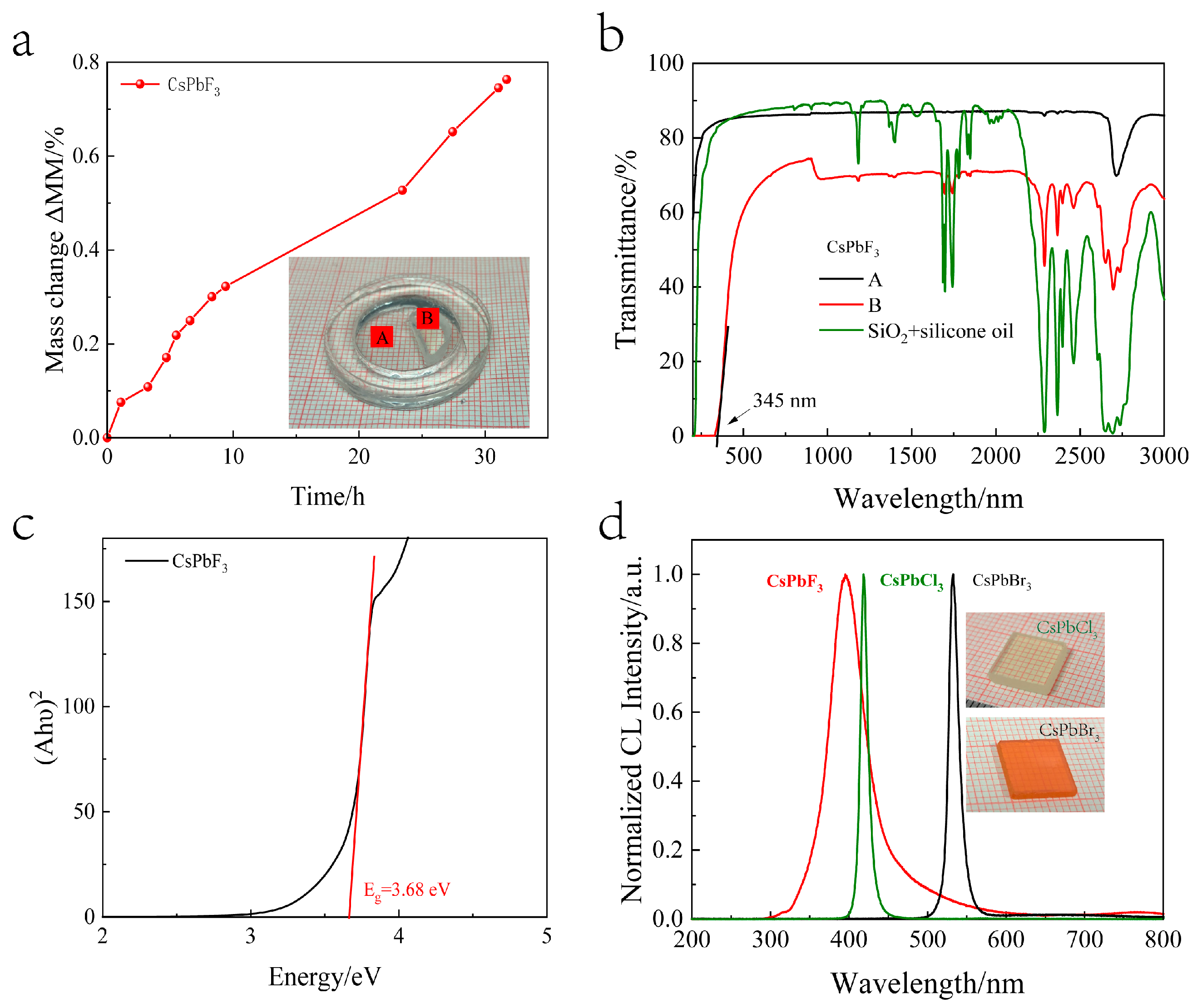
3.2. Optical Properties

The CsPbF3 crystal is known to be hygroscopic in air. In Figure 4a, the mass variation of the crystal as a function of time is presented. During the experiment, the CsPbF3 crystal was exposed to air for 30 h, and its mass increased by 0.8% as a result of its hygroscopic nature. This result highlights the high sensitivity of the crystal to hygroscopicity, emphasizing the importance of encapsulating crystals for any application. To prevent hygroscopicity, the crystals were encapsulated in a quartz box that was filled with nitrogen. Silicone oil coupling was utilized between the quartz windows and the crystal to enhance light collection. Encapsulation has been shown to be an effective method for preventing hygroscopicity, and this packaging technique is both straightforward and efficient.
In order to characterize the optical quality of the single crystal, the transmission spectrum from 200 to 3000 nm is shown in Figure 4b. The black curve corresponds to the A region in Figure 4a, which is equivalent to the cavity between two quartz windows. This structure forms a Fabry–Perot resonator with a lower transmission spectrum compared to the quartz plates. The absorption peak at around 2730 nm is related to OH-. The transmission spectrum of the A region is also used as a background to analyze the transmission spectrum of the encapsulated crystal. The red curve corresponds to the B region in Figure 4a, which is the transmission spectrum of the encapsulated CsPbF3 sample. The jump of transmittance at 800 nm is attributed to the detector shift of the spectrometer. The transmittance of CsPbF3 is more than 70% from 800 to 3000 nm, and the absorption edge is around 345 nm. The infrared absorption peak in zone B corresponds to the transmission spectrum of the quartz windows and silicone oil (blue line). Meanwhile, the Tauc Plot method was used to calculate the optical bandgap, as shown in Figure 4c. The bandgap of the CsPbF3 crystal is about 3.68 eV, indicating it is a wide bandgap semiconductor. This result is consistent with the calculation results reported [13].
Figure 4d shows CL spectra of CsPbX3 (X = F, Cl, and Br) crystals grown by the Bridgman method. The pictures of CsPbCl3 and CsPbBr3 are also shown in the plot. CsPbCl3 is a light-yellow transparent crystal, and CsPbBr3 is an orange transparent crystal. The CL spectra show the emission wavelengths of CsPbF3, CsPbCl3, and CsPbBr3 are 400 nm, 419 nm, and 534 nm, respectively. They correspond to their direct radiative transitions between the conduction band and valence band. Meanwhile, it demonstrates that the regulation of anions can achieve tunability of the emission wavelength. The full width at half maximum (FWHM) of emission peaks obtained from Gaussian fitting are 54 nm, 12 nm, and 14 nm, respectively. The FWHM value of the CsPbF3 emission peak is larger than that of CsPbCl3 and CsPbBr3, which may be due to spectral broadening induced by crystal surface deterioration.
Figure 5a shows the fluorescence excitation and emission spectra of the CsPbF3 crystal. The excitation wavelength is 208 nm, and the emission peak is around 400 nm, which is consistent with the CL spectrum. Figure 5b displays the fluorescence decay curve of the emission spectrum of CsPbF3 using an excitation wavelength of 300 nm and a monitoring wavelength of 400 nm. The green curve represents the fluorescence decay kinetic curve, and the black line represents the instrument response coefficient. The instrument response coefficient is subtracted by the inverse convolution function. The fitting results indicate that there are three decay components with decay times of 0.4 ns, 2.4 ns, and 15.0 ns, accounting for 30.4%, 50.9%, and 18.7%, respectively. This suggests that the fluorescence luminescence of CsPbF3 is fast. Compared to thin films, perovskite single crystals exhibit a stronger self-absorption effect due to the longer optical path photons take within the crystal, which increases the probability of non-radiative transitions. In the previous works, it was also observed that the PL lifetime of CsPbBr3 single crystals was shorter than that of thin film samples [27,28].
Figure 5c,d show the X-ray excited luminescence properties of the CsPbF3 crystal. In Figure 5c, the crystal emits light with a slightly redshifted wavelength of 405 nm under X-ray excitation, which is attributed to the self-absorption effect. In Figure 5d, the decay kinetic curve of CsPbF3 crystal excited by the pulsed X-ray is presented. The fitting results indicate that there are two decay components with decay times of 2.2 ns and 10.2 ns. These decay components have a good correspondence with the fluorescence decay components and indicate the potential of CsPbF3 in scintillation luminescent materials.

3.3. Electrical Properties

Figure 6a shows the Current-Voltage (I-V) curve of an ohmic type Au/CsPbF3/Au device, where the thickness of the crystal is 2 mm. The I-V curve provides valuable information on the electrical behaviors of the material, as it shows the relationship between the current flowing through the device and the voltage applied to it. In this case, the resistance of the sample is found to be approximately 2 × 10⁵ Ω, which can be inferred from the slope of the I-V curve at different voltage points. Interestingly, the cyclic I-V curve reveals that the forward scanning curve does not coincide with the reverse scanning curve. This hysteresis effect suggests that the electrical response of the material is not reversible and may be influenced by various mechanisms such as ferroelectric properties, ion vacancy migration, and so on. Although the cubic CsPbF3 does not exhibit ferroelectricity, the hysteresis effect observed in the I-V curve is believed to be related to ion migration, which may be influenced by factors such as defects, impurities, and other material parameters.
Figure 6b depicts the Current-Time (I-T) curve of the CsPbF3 single crystal under a bias voltage of 2 V, which was employed to determine the ionic and electron conductivities using the DC voltage method. The I-T curve can be separated into three stages, which are dominated by ionic migration, dominated by electron migration, and solely electron migration. The calculated ion conductivity and electron conductivity are 1.1 × 10⁻⁵ s/cm and 5.86 × 10⁻⁷ s/cm, respectively, indicating that the I-V curve hysteresis effect is linked to fluoride ion migration. The phenomenon of fluoride ion migration is commonly observed in other fluoride materials, including PbF2, SrF2, BaF2, and PbSnF4, which are all considered fluoride ion conductors. Fast ion conductors have also been discovered in gas detectors and solid electrolyte batteries. CsPbF3 is a fast ionic conductor, and its perovskite structure’s tolerance factor is located at the boundary of a stable structure. Due to the small ion radius of fluoride ions, they can move freely within the perovskite skeleton created by Pb2+, resulting in fluoride ion migration. CsPbCl3 and CsPbBr3 also exhibit ion migration, which has been exploited in research fields such as photon artificial synapses and memristors [29,30].
The intrinsic instability of perovskite materials towards water, oxygen, and temperature is primarily accountable for their inferior stability. Therefore, before characterizing the electrical performance of the CsPbF3 device, a packaging process was employed, in which the crystal was enclosed with resin casting. The devices that were not electrically tested exhibited insignificant changes in their crystal structure for a duration of one month. Conversely, the electrodes of devices that were exposed to the bias experienced marked blackening owing to direct contact with the perovskite layer. The exposure of the device to a high-voltage environment instigated electrode decomposition, and the corrosion of the gold electrode by the migration of perovskite ions resulted in apparent discoloration. Hence, the investigation of CsPbF3 stability is an essential research field.

4. Conclusions

This investigation reports the preparation of CsPbF3 single crystal by the Bridgman method. The optical and electrical properties of the synthesized crystal were characterized. The crystal was found to have a band gap of 3.68 eV, a PL emission wavelength of approximately 400 nm, and a fluorescence lifetime with three components: 0.4 ns, 2.4 ns, and 15.0 ns. It was also observed that the CsPbF3 single crystal had a high density and excellent photon cut-off ability. Under pulsed X-ray excitation, the decay times were measured to be 2.2 ns and 10.2 ns, indicating its potential as an ultrafast scintillation crystal. However, it was also noted that CsPbF3 is prone to being hygroscopic and exhibits high ion mobility. These properties make CsPbF3 single crystals promising candidates for various applications, such as ultrafast scintillation materials or visible-blind photoelectric detection devices and more.

Author Contributions

X.Y. and F.Y. conceived the idea and designed the experiments. X.Y., C.G., K.D. and S.L. participated in the crystal growth and preparation. X.Y., C.P., X.H., H.H. and Z.S. performed the device characterization and simulation. B.X., Y.J., R.W., K.Z., Y.L. and W.D. analyzed the data and contributed to the mechanism investigation. X.Y. and F.Y. wrote the manuscript. All authors participated in the discussion and commented on the manuscript. All authors have read and agreed to the published version of the manuscript.

Funding

This research was funded by the National Key R&D Program of China, grant number 2022YFB3503901, the National Natural Science Foundation of China under Grant 12175110, 11775120, 11535010, and Foundation of State Key Laboratory of Intense Pulsed Radiation Simulation and Effect under Grant SKLIPR1805.

Conflicts of Interest

The authors declare no conflict of interest. The funders had no role in the design of the study; in the collection, analyses, or interpretation of data; in the writing of the manuscript; or in the decision to publish the results.

References

  1. Liu, X.; Li, J.; Wang, X.; Yang, D. Inorganic lead-based halide perovskites: From fundamental properties to photovoltaic applications. Mater. Today 2022, 61, 191–217. [Google Scholar] [CrossRef]
  2. Chen, Y.; Feng, Z.; Pal, A.; Zhang, J. Recent Progress on the Performance of Lead-Based Halide Perovskite APbX3 Detectors. Phys. Status Solidi A 2022, 219, 2200018. [Google Scholar] [CrossRef]
  3. Xu, J.; Maxwell, A.; Wei, M.; Wang, Z.; Chen, B.; Zhu, T.; Sargent, E.H. Defect Tolerance of Mixed B-Site Organic-Inorganic Halide Perovskites. ACS Energy Lett. 2021, 6, 4220–4227. [Google Scholar] [CrossRef]
  4. Worku, M.; Ben-Akacha, A.; Blessed Shonde, T.; Liu, H.; Ma, B. The Past, Present, and Future of Metal Halide Perovskite Light-Emitting Diodes. Small 2021, 1, 2000072. [Google Scholar] [CrossRef]
  5. Tian, J.; Xue, Q.; Yao, Q.; Li, N.; Brabec, C.J.; Yip, H.L. Inorganic Halide Perovskite Solar Cells: Progress and Challenges. Adv. Energy Mater. 2020, 10, 2000183. [Google Scholar] [CrossRef]
  6. Tao, S.; Schmidt, I.; Brocks, G.; Jiang, J.; Tranca, I.; Meerholz, K.; Olthof, S. Absolute energy level positions in tin- and lead-based halide perovskites. Nat. Commun. 2019, 10, 2560. [Google Scholar] [CrossRef]
  7. He, Y.; Hadar, I.; Kanatzidis, M.G. Detecting ionizing radiation using halide perovskite semiconductors processed through solution and alternative methods. Nat. Photonics 2021, 16, 14–26. [Google Scholar] [CrossRef]
  8. Ahmad, W.; Khan, J.; Niu, G.; Tang, J. Inorganic CsPbI3 Perovskite-Based Solar Cells: A Choice for a Tandem Device. Solar RRL 2017, 1, 1700048. [Google Scholar] [CrossRef]
  9. Tan, S.; Yu, B.; Cui, Y.; Meng, F.; Huang, C.; Li, Y.; Chen, Z.; Wu, H.; Shi, J.; Luo, Y.; et al. Temperature-Reliable Low-Dimensional Perovskites Passivated Black-Phase CsPbI3 toward Stable and Efficient Photovoltaics. Angew. Chem. Int. Ed. Engl. 2022, 61, e202201300. [Google Scholar] [CrossRef]
  10. Yuan, S.; Wang, Z.K.; Zhuo, M.P.; Tian, Q.S.; Jin, Y.; Liao, L.S. Self-Assembled High Quality CsPbBr3 Quantum Dot Films toward Highly Efficient Light-Emitting Diodes. ACS Nano 2018, 12, 9541–9548. [Google Scholar] [CrossRef]
  11. He, Y.; Petryk, M.; Liu, Z.; Chica, D.G.; Hadar, I.; Leak, C.; Ke, W.; Spanopoulos, I.; Lin, W.; Chung, D.Y.; et al. CsPbBr3 perovskite detectors with 1.4% energy resolution for high-energy γ-rays. Nat. Photonics 2020, 15, 36–42. [Google Scholar] [CrossRef]
  12. He, Y.; Stoumpos, C.C.; Hadar, I.; Luo, Z.; McCall, K.M.; Liu, Z.; Chung, D.Y.; Wessels, B.W.; Kanatzidis, M.G. Demonstration of Energy-Resolved gamma-Ray Detection at Room Temperature by the CsPbCl3 Perovskite Semiconductor. J. Am. Chem. Soc. 2021, 143, 2068–2077. [Google Scholar] [CrossRef] [PubMed]
  13. Mykhaylyk, V.B.; Rudko, M.; Kraus, H.; Kapustianyk, V.; Kolomiets, V.; Vitoratou, N.; Chornodolskyy, Y.; Voloshinovskii, A.S.; Vasylechko, L. Ultra-fast low temperature scintillation and X-ray luminescence of CsPbCl3 crystals. J. Mater. Chem. C 2023, 11, 656–665. [Google Scholar] [CrossRef]
  14. Murtaza, G.; Ahmad, I.; Maqbool, M.; Aliabad, H.A.R.; Afaq, A. Structural and Optoelectronic Properties of Cubic CsPbF3 for Novel Applications. Chinese Phys. Lett. 2011, 28, 117803. [Google Scholar] [CrossRef]
  15. Bouznik, V.M.; Moskvich, Y.N.; Voronov, V.N. Nuclear magnetic resonance study of 19F motion in CsPbF3. Chem. Phys. Lett. 1976, 37, 464–467. [Google Scholar] [CrossRef]
  16. Berastegui, P.; Hull, S.; Eriksson, S.-G. A low-temperature structural phase transition in CsPbF3. J. Phys. Condens. Matter. 2001, 13, 5077–5088. [Google Scholar] [CrossRef]
  17. Smith, E.H.; Benedek, N.A.; Fennie, C.J. Interplay of Octahedral Rotations and Lone Pair Ferroelectricity in CsPbF3. Inorg. Chem. 2015, 54, 8536–8543. [Google Scholar] [CrossRef]
  18. Wang, J.; Hao, J.; Duan, C.; Wang, X.; Wang, K.; Ma, C. A Fluoride-Ion-Conducting Solid Electrolyte with Both High Conductivity and Excellent Electrochemical Stability. Small 2022, 18, e2104508. [Google Scholar] [CrossRef]
  19. Song, J.; Cui, Q.; Li, J.; Xu, J.; Wang, Y.; Xu, L.; Xue, J.; Dong, Y.; Tian, T.; Sun, H.; et al. Ultralarge All-Inorganic Perovskite Bulk Single Crystal for High-Performance Visible-Infrared Dual-Modal Photodetectors. Adv. Opt. Mater. 2017, 5, 1700157. [Google Scholar] [CrossRef]
  20. Vanecek, V.; Kral, R.; Paterek, J.; Babin, V.; Jary, V.; Hybler, J.; Kodama, S.; Kurosawa, S.; Yokota, Y.; Yoshikawa, A.; et al. Modified vertical Bridgman method: Time and cost effective tool for preparation of Cs2HfCl6 single crystals. J. Cryst. Growth 2020, 533, 125479. [Google Scholar] [CrossRef]
  21. Zhang, P.; Zhang, G.; Liu, L.; Ju, D.; Zhang, L.; Cheng, K.; Tao, X. Anisotropic Optoelectronic Properties of Melt-Grown Bulk CsPbBr3 Single Crystal. J. Phys. Chem. Lett. 2018, 9, 5040–5046. [Google Scholar] [CrossRef] [PubMed]
  22. Charles, B.; Dillon, J.; Weber, O.J.; Islam, M.S.; Weller, M.T. Understanding the stability of mixed A-cation lead iodide perovskites. J. Mater. Chem. A 2017, 5, 22495–22499. [Google Scholar] [CrossRef]
  23. Li, Z.; Yang, M.; Park, J.S.; Wei, S.H.; Berry, J.J.; Zhu, K. Stabilizing Perovskite Structures by Tuning Tolerance Factor: Formation of Formamidinium and Cesium Lead Iodide Solid-State Alloys. Chem. Mater. 2015, 28, 284–292. [Google Scholar] [CrossRef]
  24. Straus, D.B.; Guo, S.; Cava, R.J. Kinetically Stable Single Crystals of Perovskite-Phase CsPbI3. J. Am. Chem. Soc. 2019, 141, 11435–11439. [Google Scholar] [CrossRef] [PubMed]
  25. Zhao, L.; Zhou, Y.; Shi, Z.; Ni, Z.; Wang, M.; Liu, Y.; Huang, J. High-yield growth of FACsPbBr3 single crystals with low defect density from mixed solvents for gamma-ray spectroscopy. Nat. Photonics. 2023, 17, 315–323. [Google Scholar] [CrossRef]
  26. Kobayashi, M.; Omata, K.; Sugimoto, S.; Tamagawa, Y.; Kuroiwa, T.; Asada, H.; Takeuchi, H.; Kondo, S. Scintillation characteristics of CsPbCl3 single crystals. Nucl. Instrum. Methods. Phys. Res. B 2008, 592, 369–373. [Google Scholar] [CrossRef]
  27. Li, C.; Zang, Z.; Han, C.; Hu, Z.; Tang, X.; Du, J.; Leng, Y.; Sun, K. Highly compact CsPbBr3 perovskite thin films decorated by ZnO nanoparticles for enhanced random lasing. Nano Energy 2017, 40, 195–202. [Google Scholar] [CrossRef]
  28. Pan, L.; Pandey, I.R.; Miceli, A.; Klepov, V.V.; Chung, D.Y.; Kanatzidis, M.G. Perovskite CsPbBr3 Single-Crystal Detector Operating at 1010 Photons s−1 mm−2 for Ultra-High Flux X-ray Detection. Adv. Opt. Mater. 2023, 11, 2202946. [Google Scholar] [CrossRef]
  29. Yang, L.; Singh, M.; Shen, S.W.; Chih, K.Y.; Liu, S.W.; Wu, C.I.; Chu, C.W.; Lin, H.W. Transparent and Flexible Inorganic Perovskite Photonic Artificial Synapses with Dual-Mode Operation. Adv. Funct. Mater. 2020, 31, 2008259. [Google Scholar] [CrossRef]
  30. Wu, Y.; Wei, Y.; Huang, Y.; Cao, F.; Yu, D.; Li, X.; Zeng, H. Capping CsPbBr3 with ZnO to improve performance and stability of perovskite memristors. Nano Res. 2016, 10, 1584–1594. [Google Scholar] [CrossRef]
Figure 1. Schematic illustration of the crystal growth using the vertical Bridgman method.
Crystals 13 00765 g001
Figure 2. (a) Linear attenuation coefficients as a function of photon energy for several fast scintillation crystals. (b) The relationship between cubic transition temperature and Goldschmidt tolerance factor. (c) A transition of CsPbF3 from a rhombohedral distorted perovskite structure to a cubic perovskite structure at 187 K.
Crystals 13 00765 g002
Figure 3. (a) DTA (black line) and TG curves (red line) of the CsPbF3 crystal. (b) Photograph of CsPbF3 single crystal. (c) Powder XRD pattern of the CsPbF3 crystal and standard PDF card (ICDD 22-1075) of the CsPbF3 crystal. (d) Cleavage surface XRD pattern of the CsPbF3 crystal.
Crystals 13 00765 g003
Figure 4. (a) The weight of the crystal changes with time. (b) Optical transmission spectrum of the CsPbF3 crystal. (c) The band gap of the sample was calculated by the Tauc Plot method. (d) Cathodoluminescence spectrum of the CsPbX3 (X = F, Cl and Br) crystals.
Crystals 13 00765 g004
Figure 5. (a) Photoluminescence excitation and emission spectra of CsPbF3 crystal. (b) Photoluminescence decay curve of CsPbF3 crystal (Excitation: 300 nm; Emission: 400 nm). (c) X-ray emission spectra of CsPbF3 crystal. (d) Decay kinetics curve excited by the pulsed X-ray.
Crystals 13 00765 g005
Figure 6. (a) Current-Voltage and (b) Current-Time characteristic curves of an ohmic type Au/CsPbF3/Au device.
Crystals 13 00765 g006
Disclaimer/Publisher’s Note: The statements, opinions and data contained in all publications are solely those of the individual author(s) and contributor(s) and not of MDPI and/or the editor(s). MDPI and/or the editor(s) disclaim responsibility for any injury to people or property resulting from any ideas, methods, instructions or products referred to in the content.

