Abstract
In this study, the performance of Schottky barrier diodes (SBD) based on β-Ga2O3 with floating metal rings (FMR) was investigated using numerical simulations with Technology Computer-Aided Design (TCAD) software. The simulation parameters of β-Ga2O3, including those in barrier lowering, impact ionization, and image-force-lowering models, were extracted from experimental results. Similar forward conduction characteristics to SBDs without FMRs were exhibited by the device, and its breakdown characteristics were influenced by structural parameters such as FMR spacing, width, number, epitaxial layer thickness, and doping concentration. A breakdown voltage of 2072 V was achieved by the optimized device at a doping concentration of 1016 cm−3, which was 2.5 times higher than that of a device without FMRs. This study also indicated that for general doping concentrations and epitaxial layer thicknesses, the breakdown voltage with such structures can reach at least 1.5 times higher than that of a device without FMRs. Overall, insights into optimizing the design of β-Ga2O3-based SBDs with FMRs were provided in this study.
1. Introduction
Beta-phase gallium oxide (β-Ga2O3) is widely used as an ultra-wide bandgap semiconductor and for power electronics due to its wide bandgap (4.8 eV) [1], large critical electric field (~8 MV) [2], high Baliga’s figure of merit (BFOM) [3], and varying electron doping concentrations ranging from 1014 cm−3 to 1020 cm−3 [4]. Schottky barrier diodes (SBD) based on β-Ga2O3 are widely used in photodetectors (PD) [5,6] and power rectifiers [7,8]. To gain a larger breakdown voltage (BV) for power devices, edge terminations are introduced [8,9,10,11,12,13,14,15]. The field plate is a common method that originated in field effect transistors (FET) [9,10,14] and was borrowed by SBDs [11,12,13,15]. Such structures require a high level of fabrication techniques, which may cause damage to the β-Ga2O3 epitaxy film [15,16]. Another method commonly used is introducing p-type doping to form floating field rings (FFR) [17,18]. However, the difficulty in realizing p-type doping [19,20], usually needs a heterojunction for β-Ga2O3-based devices [21,22]. To overcome such difficulties, FMR is introduced, replacing floating p-n junctions with floating metal-semiconductor junctions [23,24]. Previous studies have focused on the structure fabrication process, but with little structure improvement, especially with numerical computation.
The low-cost method of numerical computation has been widely used for designing devices and researching the performance of various new materials and devices [25,26,27]. However, the poor convergence of numerical computation for β-Ga2O3 devices is currently a problem due to the ultra-wide bandgap of β-Ga2O3, which leads to a low intrinsic carrier concentration. Furthermore, the basic material parameters of β-Ga2O3 are not well-defined, and the default values in numerical computation cannot be coupled with other parameters. Material parameters can be obtained through various methods, such as first principles [28] and force fields [29], but these methods are overly idealized and do not account for the influence of defects in material growth and device preparation on the material parameters. Material parameters can also be obtained through material characterization, such as measuring the bandgap width through absorption spectroscopy [30]. However, these parameters still ignore the degradation of material performance during device fabrications [31]. Material parameters extracted from device performance through experimentation can better simulate device performance [32,33,34], similar to post-simulation in circuit design [35,36,37,38], which can consider non-ideal effects.
In this study, the material parameters of β-Ga2O3 (<001> orientation), including the constant mobility, the impact ionization coefficients (IIC), and the parameters for image force lowering (IFL) and tunneling effect (TE) for electrons and holes [39], were extracted and analyzed using Synopses Sentaurus TCAD software. The forward and reverse characteristics of devices with different structural configurations were simulated using the extracted parameters. The forward characteristics of SBDs with FMRs and those without were compared, and the effects of five structural parameters of FMR on breakdown characteristics, including FMR spacing, FMR width, number of FMRs, epitaxial doping concentration, and epitaxial thickness, were analyzed. Electric field (E-Field) distributions were provided, and the effects of each structural parameter on electric field distribution and breakdown voltage were qualitatively analyzed. Finally, suggestions were given for the practical utilization of this structure.
2. Simulation Setup
The simulation of SBD requires the use of various physical models that accurately reflect the intrinsic characteristics of the device’s materials. Although material science has provided many parameters for device simulation, the process of device fabrication will introduce defects, leading to significant discrepancies between calculated parameters and actual device performance [16]. To improve accuracy, the parameters in this article were directly extracted from experimental results in reference [13].
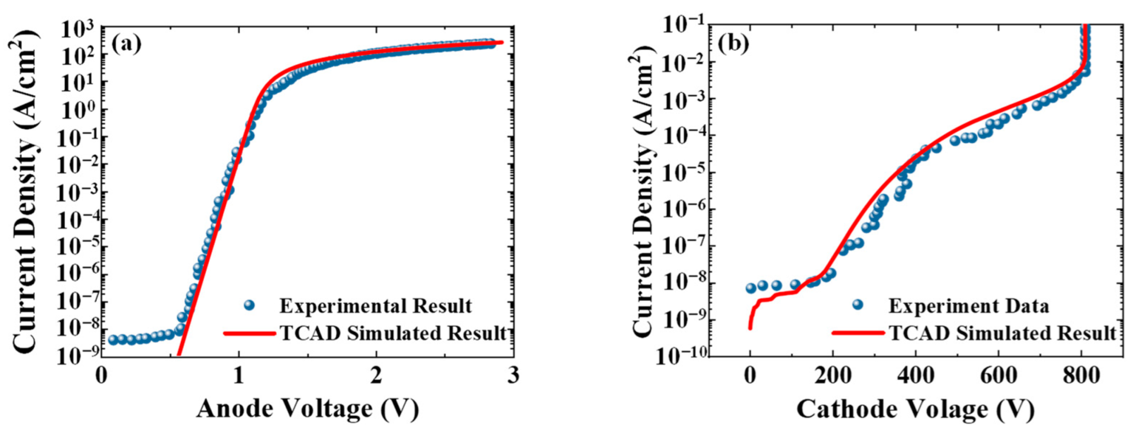
The constant mobility μ is obtained from the forward characteristics of an SBD, and the simulation results are presented in Figure 1a. The value of electron mobility is relatively low in our simulation. This is because β-Ga2O3 is a semiconductor material with relatively low intrinsic mobility, typically around 100 cm2/V∙s. Moreover, the presence of defects and vacancies during the fabrication process can further degrade the material’s mobility [40,41]. The reverse characteristics of an SBD are mainly governed by tunneling, impact ionization, and barrier lowering [39], and the nonlocal tunneling model (NLM), barrier-lowering model, and van Overstraeten-de Man model are used, respectively. Those models are described as follows:

Figure 1.
Extraction results of simulation parameters (a,b). Forward and reverse characteristics of the device with both the experimental results from reference [13] and the simulated results: (a) forward characteristics and (b) reverse characteristics.
NLM is described by Formula (1), where G is the carrier generation rate due to tunneling, g is a fitting parameter, A* is the Richardson constant for electrons in β-Ga2O3, T is the Temperature the device working at, F is the electric field intensity, kB is the Boltzmann constant, r is the distance variable, E(r) is the distance carrier energy, mainly electron in β-Ga2O3, mh and me are effective mass of electron and hole, respectively, P is the tunneling probability based on the effective mass of electrons and holes, ES is the quasi-Fermi level in the semiconductor, and EM is the Fermi level in the metal. The barrier-lowering model is described by Formula (2), where ΔΦb is the barrier-lowering value, a and p are fitting parameters, E is the electric field intensity, E0 is the reference electric field given the value of 1 V/cm here for easier calculations, and Eeq is the electric field intensity at equilibrium. Van Overstraeten-de Man model is described by Formula (3), where αn,p represents the ionization rate coefficients for electrons and holes, E is the electric field intensity, and an,p, and bn,p are two fitting parameters [42]. All simulation parameters are presented in Table 1, which are obtained from simulation results presented in Figure 1b.

Table 1.
Material simulation parameter table.
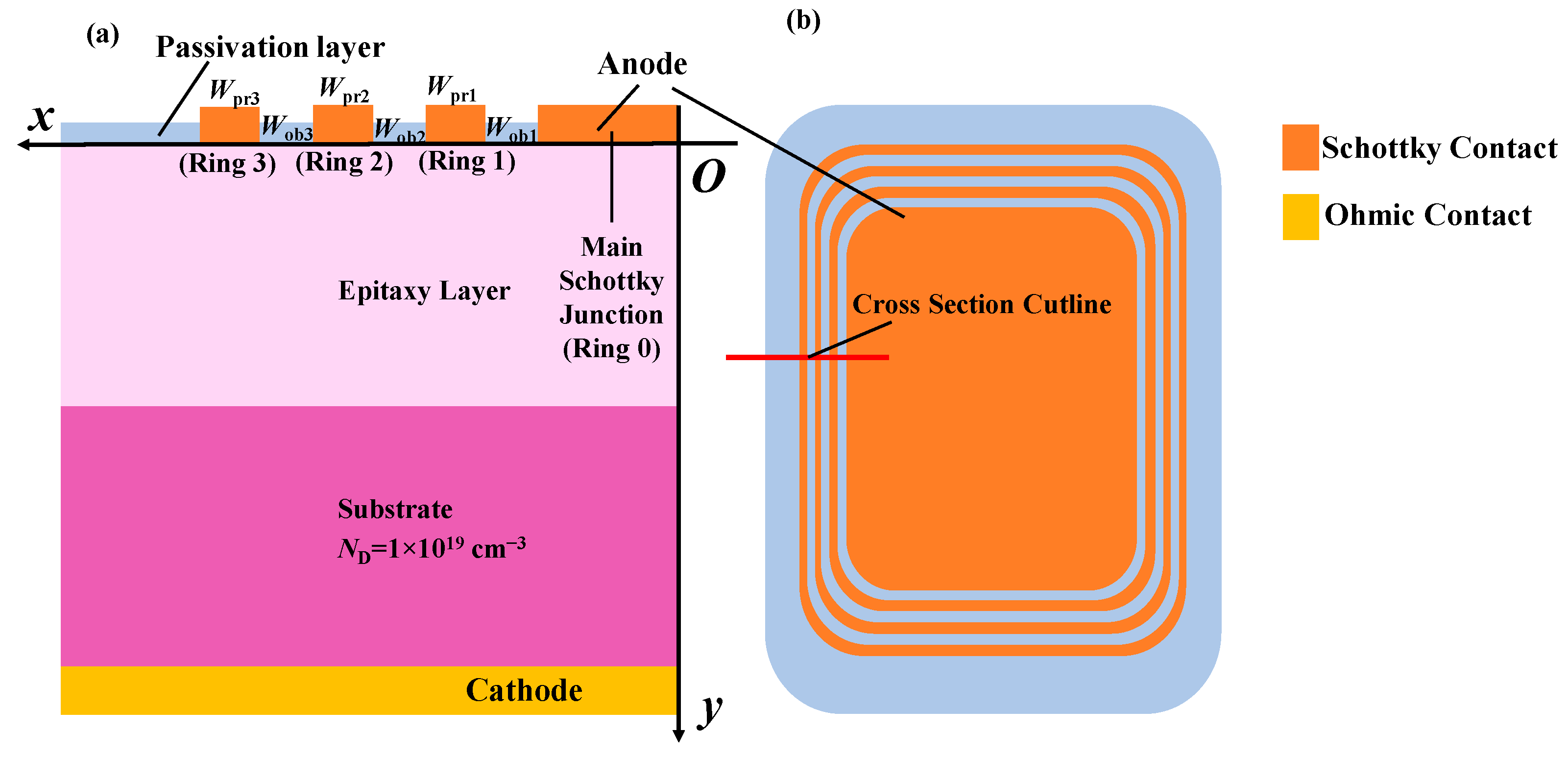
The SBD structure used in this study is shown in Figure 2. The structure consists of a high-doped n-type substrate with a doping concentration of 1019 cm−3, and its thickness was fixed at 10 μm. A low-doped n-type epitaxial layer was grown on the top of the substrate, and the doping concentration and epitaxial layer thickness were set as structural variables. The electron affinity in β-Ga2O3 was set as 4 eV. The cathode at the bottom of the substrate was defined by an ohmic junction, and the anode at the top of the epitaxial layer was defined by a Schottky junction. In this work, simulated devices share a relatively large size, and the electrode shape’s impact on the device performance in the proposed device structure is minimal. Thus, a 3D structure can be transferred into a 2D simulation [43,44]. The FMR structure was placed outside the anode and defined by the Schottky junction. The height of the anode and FMRs was set as 100 nm. The work function of anode and FMRs metal was defined as 5.3 eV. The anode and the cathode are directly connected to the applied voltage, while FMRs are floating electrodes with no voltage applied. The number of FMRs, the width of each FMR, and the spacing between adjacent FMRs were set as structural variables. The surface passivation layer on the top of the SBD was set as Al2O3. The spacing, width, and number of FMRs vary from 1 to 10 μm, 1 to 10 μm, and 0 to 10, respectively. Structural variables were named, as shown in Table 2.

Figure 2.
Device structure of SBD with FMR, where main SBD is connected directly to the ground or applied voltage, while FMRs are floating electrodes. (a) Cross-sectional view of the device with 3 FMRs. (b) Top view of the device with 3 FMRs.

Table 2.
Structural simulation parameter table.
3. Results and Discussions
3.1. Forward Characteristics
The forward characteristics of Schottky barrier diodes (SBDs) with different FMR structural parameters were studied. The results are shown in Figure 3. In Figure 3a, the forward characteristics of structures with different numbers of FMRs were displayed, where the ring spacing and width between all rings were set to 1 μm. It can be seen that there is no significant difference between the three structures. Figure 3b,c shows the forward characteristics of SBDs with only one FMR and the effects of ring width and ring spacing on the forward characteristics, respectively. It can be observed from the figures that changing the ring width and ring spacing does not affect the forward characteristics of the SBD.

Figure 3.
Forward voltage–current characteristics of SBD: (a) with different numbers of FMR, (b,c) with single FMR, (b) with different ring spacing, and (c) with different ring widths.
The following theory is used to explain this phenomenon. The forward characteristics mechanism of β-Ga2O3-based SBDs is as follows: the epitaxial layer is depleted, and a potential barrier is formed due to the difference in the Schottky metal’s work function. In our simulation, the working principle of the SBD can be explained using the thermal ion emission theory as follows [5]:
where I0 is the reverse saturation current, q is the electronic charge (1.6 × 10⁻¹⁹ C), n is the ideality factor, k is the Boltzmann constant (1.38 × 10⁻²³ J/K), T is the temperature, A is the contact area between the metal electrode and the semiconductor, and φb is the Schottky barrier height (SBH). SBH, A* is the Richardson constant, A is the electrode area, and m* is the effective mass of β-Ga2O3, which is considered 0.324m0, where m0 is the mass of a free electron. For β-Ga2O3, A* is estimated to be approximately 41 A/cm2K2. According to the above theory, the forward characteristics of the device are only related to the height of the potential barrier between the metal and semiconductor materials and are not affected by the device structure. As the forward current increases, the differential resistance of the SBD can be calculated as Rs, which can be described as follows [45]:
where the resistivity ρs is directly related to the carrier mobility μn,p. In our designed device structure, the area of the Schottky junction does not change, and at low voltages, the external FMR has little effect on the main Schottky junction. Therefore, the introduction of FMRs does not change the forward characteristics of the device.
3.2. Relationship between Breakdown Voltage and FMR Spacing
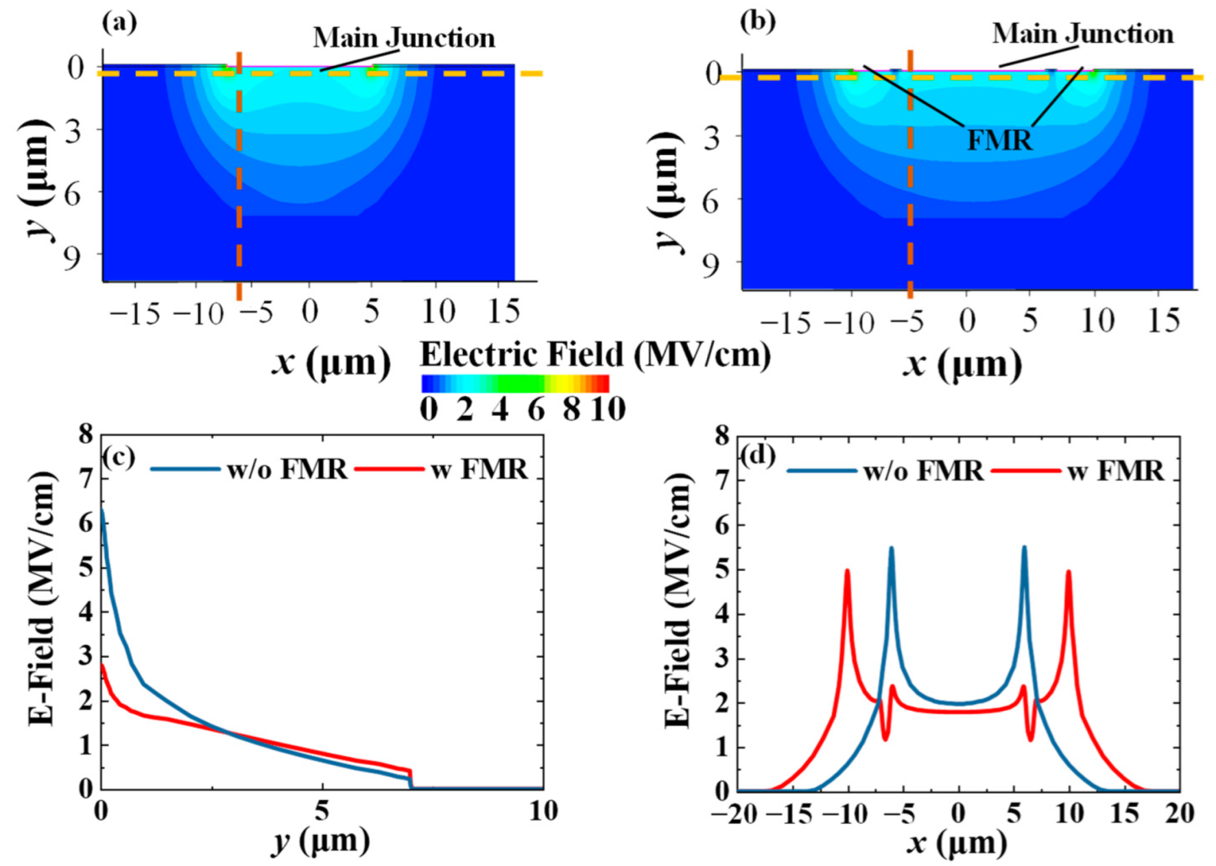
The basic principle of FMRs is to lower the peak electric field intensity at the edge of the Schottky junction by extending the depletion region formed at the junction; meanwhile, FMR will reduce the slope of the electric field intensity in the drift region, thereby increasing the breakdown voltage [46], as shown in Figure 4.

Figure 4.
The electric field at 810 V. (a,b)The 2D distribution (a) without FMR and (b) with FMR. (c) Vertical cutline profile in (a,b). (d) Lateral cutline profile in (a,b).
Figure 4a displayed the electric field distribution at 810 V for the SBD structure with an epitaxial thickness of 7 μm and an epitaxial layer doping concentration of 1016 cm−3 without the FMR structure. Figure 4b displayed the same structure as the FMR structure at the same voltage. Figure 4c,d gives the vertical and lateral profile of the electric field. It is shown that the peak electric field of the main Schottky junction is substantially lower, while the peak electric field of the FMR edge is still lower than that of the peak electric field without the FMR structure. With the help of FMR, the breakdown voltage of the structure in Figure 4a is 810 V and in Figure 4b is 1258 V, which is 1.5 times higher than without FMR.
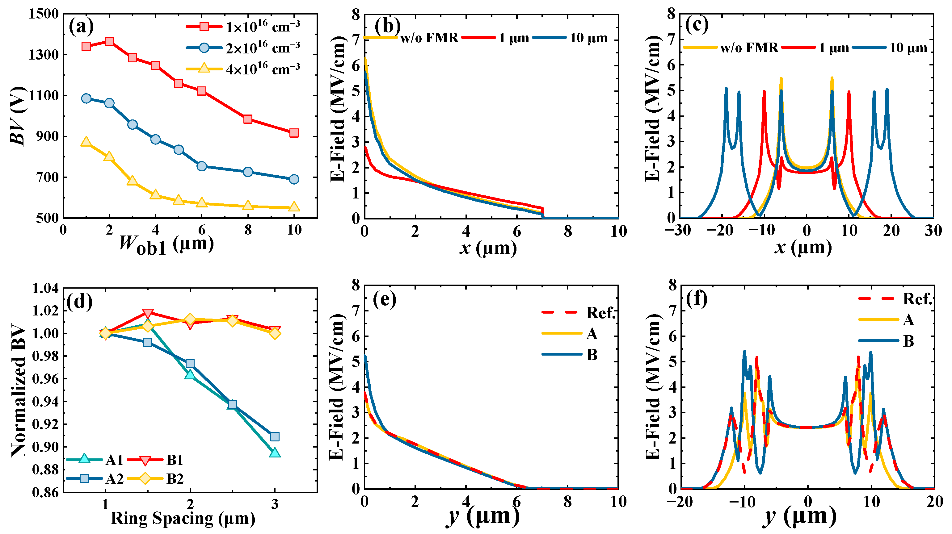
The relationship between breakdown voltage and spacings between FMRs and the main Schottky junction was first studied. To simplify our discussion, only one-FMR and two-FMR cases were discussed. Figure 5 shows the simulation results for relevant structures with the structural parameters of Lepi = 7 μm. In the one-FMR case, as the spacing increases, the breakdown voltage gradually decreases until it finally drops to the same level as that of no FMR, as shown in Figure 5a. This is because, with larger spacing, the FMR will have less effect on the electric field distribution at the edge of the main Schottky junction, as shown in Figure 5c. When another FMR is added, the inner spacing has more influence on the breakdown voltage than the outer one, as shown in Figure 5d, where structures in group A were changing the inner spacing and those in group B were changing the outer one. The reference value of the normalized breakdown voltages in Figure 5d. is 1475 V with Nepi = 1016 cm−3 for A1 and B1 and 1238 V for A2 and B2 with Nepi = 2 × 1016 cm−3. The device structure used for the normalization breakdown voltage had inner and outer FMRs with a width of 1 μm and an inter-FMR spacing of 1 μm. The inner and outer inter-FMR spacings were varied for the other devices. The outer spacing also influences the breakdown voltage, which, however, is minute. The effect of the outer FMR can be understood as an independent FMR optimizing the electric field distribution at the edge of the main Schottky junction. The outer FMR is already in a position where the impact on the breakdown voltage is minimal. However, it should be noted that the outer FMR will optimize the electric field distribution at the edge of the inner FMR, as electric field profile shown in Figure 5f. So, spacings between the FMRs as small as possible are still needed to reduce the peak electric field intensity at the edge of the inner FMR.
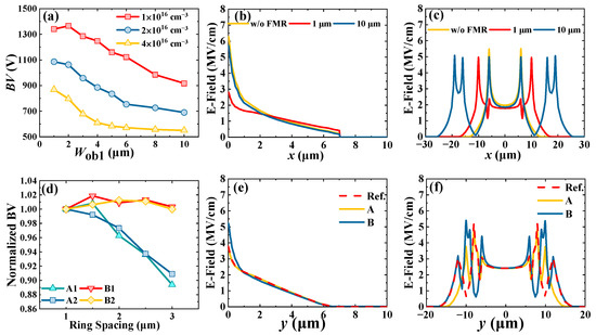
Figure 5.
Relationship between breakdown voltage and FMR spacing. (a–c) Single FMR, (a) breakdown voltage decreases as FMR spacing increases; (b,c) electric field distribution at the breakdown, (b) vertical profile, and (c) lateral profile. (d,f) Double FMRs; (d) inner spacing has a greater effect on breakdown voltage than outer spacing; (e,f) electric field distribution at 810 V; (e) vertical profile; and (f) lateral profile.
3.3. Relationship between Breakdown Voltage and FMR Width
The relationship between breakdown voltage and FMR width was further studied. Figure 6 shows the simulation results for the relevant structures with the structural parameters of Lepi = 7 μm. Additionally, to simplify our discussion, only one-FMR and two-FMR cases were discussed then. In one-FMR case, as the FMR width increases, the breakdown voltage remains stable, as shown in Figure 6a. This is because the increase in FMR width does not change the spacing between the FMR and the edge of the main Schottky junction, and the influence to change the electric field intensity at the main Schottky junction edge is not significant, so the change in breakdown voltage is not significant, as shown in Figure 6c.
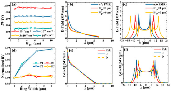
Figure 6.
Relationship between breakdown voltage and FMR width. (a–c) Single FMR, (a) FMR width has little effect on the breakdown voltage; (b,c) Electric field distribution at 810 V, (b) vertical profile, and (c) lateral profile. (d–f) Double FMRs; (d) the inner FMR width has a greater effect on the breakdown voltage; (e,f) electric field distribution at 810 V; (e) vertical profile; and (f) lateral profile.
Figure 6d shows the effect of changing the inner and outer FMR widths on the breakdown voltage, where structures in group C were changing the inner FMR width and those in group D were changing the outer FMR width. The reference value of the normalized breakdown voltages in Figure 6d is 1475 V with Nepi = 1016 cm−3 for C1 and D1 and 1238 V for C2 and D2 with Nepi = 2 × 1016 cm−3. The device structure used for the normalization breakdown voltage has inner and outer FMR with a width of 1 μm and an inter-FMR spacing of 1 μm. The inner and outer FMR widths were varied for the other devices. After adding a second FMR outside the inner FMR, as the width of the first FMR increases, the breakdown voltage also increases. Although the second FMR’s ability to optimize the electric field distribution at the edge of the main Schottky junction is weakened, the outer FMR still optimizes the electric field distribution at the outer edge of the inner FMR. The increase in the width of the inner FMR weakens the electric field intensity peak caused at the edge of the inner FMR. Figure 6f gives a more direct explanation of the electric field profile. Therefore, in further design, the inner FMRs should have larger FMR widths, and the FMR width should decrease from the inside to the outside.
3.4. Relationship between Breakdown Voltage and Number of FMRs
Further research on the relationship between breakdown voltage and the number of FMRs was conducted. Structures were designed according to two criteria: the spacings between FMRs should be as small as possible, and the width of the FMRs should decrease from the inside to the outside. The group with the highest breakdown voltage from all the configurations that meet these two criteria were selected. Figure 7 shows the simulation results for structures with structural parameters of Lepi = 7 μm and Nepi = 1016 cm−3. Simulation results in Figure 7a show that as the number of FMRs increases, the breakdown voltage initially increases, but, as shown in Figure 7c, once the number of FMRs reaches a certain value, the breakdown voltage no longer increases and shows a saturation trend. Here, the largest breakdown voltage is selected. As illustrated in Figure 7a, the breakdown voltage of SBD with an FMR structure reaches up to 2072 V, which is 2.5 times the breakdown voltage of 810 V without an FMR structure. Such structure has 6 FMRs structure and has an optimal combination of 1 μm inter-FMR spacing and 5 μm, 4μm, 3 μm, 3 μm, 1 μm, and 1 μm ring widths from the inside to the outside. The reference breakdown voltages in Figure 7c are the breakdown voltages of the corresponding concentration without FMRs, which are 1026 V for 5 × 1015 cm−3, 810 V for 1016 cm−3, and 689 V for 2 × 1016 cm−3.

Figure 7.
(a) As the number of FMRs increases, the breakdown voltage increases initially. (b) Vertical electric field profile at the breakdown of the device with different numbers of FMRs. (c) The breakdown voltage saturates as the number of FMRs reaches a certain value.
By comparing the electric field distribution at different numbers of FMRs, as shown in Figure 7b, it is found that as the number of FMRs increases, the slope of the electric field intensity in the drift region gradually decreases until it becomes flat. When the electric field intensity curve in the drift region becomes flat, increasing the number of FMRs cannot further optimize this electric field distribution, so the breakdown voltage reaches saturation. This process essentially redistributes the charge in the drift region and the number of FMRs; the breakdown voltage saturates and is related to the doping concentration and epitaxial layer thickness, limiting the further increase of the breakdown voltage. This will be discussed in the following sections.
3.5. Relationship between Breakdown Voltage and Doping Concentration
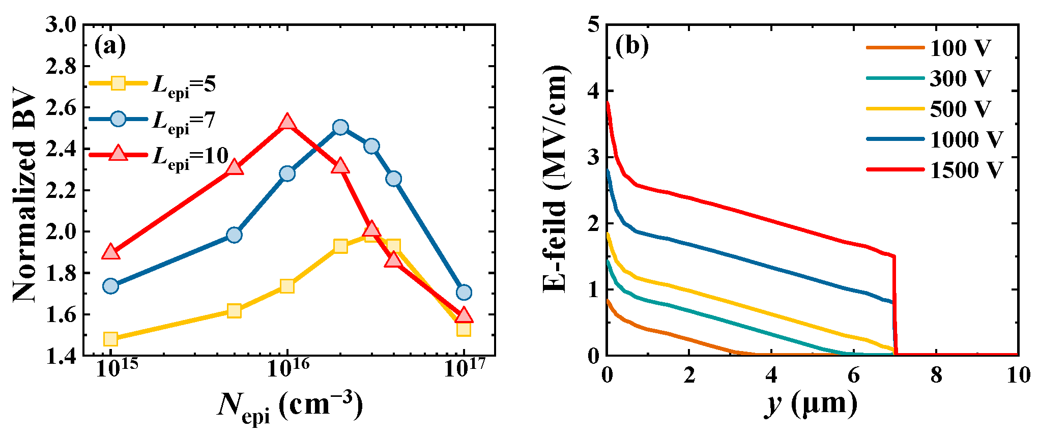
A clearer understanding of the investigation on breakdown voltage saturation was provided by examining the effect of doping concentration on the saturation of the breakdown voltage. Simulations were conducted on various structures with specific parameters of Lepi = 7 μm and 5 FMRs’ widths set as 5 μm, 3 μm, 3 μm, 2 μm, and 1 μm, respectively, with uniform spacings of 1 μm. To facilitate the comparison of the results, the breakdown voltage was normalized by dividing the saturation breakdown voltage by the breakdown voltage of the structure with no FMR at the corresponding concentration and epitaxial thickness. It is important to note that this normalization was used to accurately assess the impact of different epitaxial layer thicknesses within the specified concentration range. The investigation results indicated that the breakdown voltage initially increased and then decreased with varying epitaxial layer thicknesses within the specified concentration range. These findings provide valuable insight into the relationship between doping concentration and breakdown voltage saturation.
Figure 8b illustrates that the slope of the electric field distribution in the depletion region remains constant as the applied voltage increases. This observation leads to the question of how the slope of the electric field changes with the addition of FMRs at various concentrations. At low doping concentrations, the vertical electric field intensity has a minimal slope, which means that the depletion width, or the region where the doping concentration drops to zero, is relatively large. This results in a high breakdown voltage without the need for FMR, as shown in Figure 9a. However, adding FMR has limited effects on further reducing the slope and increasing the breakdown voltage. Consequently, the optimization effect is also limited. On the other hand, at high doping concentrations, the slope of the vertical electric field intensity is high, and the depletion width is small. Despite the addition of FMR, the change in the vertical electric field distribution is insufficient to increase the breakdown voltage significantly, as shown in Figure 9b. For intermediate concentrations, the vertical electric field intensity has a noticeable slope, and the depletion width is relatively large without FMR. Thus, as the slope of the vertical electric field intensity decreases, the breakdown voltage can increase significantly, as shown in Figure 9c. Therefore, this structure is more effective for doping concentrations around 1016 cm−3.

Figure 8.
(a) The breakdown voltages increase first and then decrease. (b) Vertical electric field profile of a given device at different voltages.

Figure 9.
Lateral electric field profile of device with and without FMR, with Nepi of (a) 1015 cm−3, (b) 1016 cm−3, (c) 1017 cm−3 at the breakdown.
3.6. Relationship between Breakdown Voltage and Epitaxial Layer Thickness
To further investigate the saturation and optimization of breakdown voltage, the relationship between breakdown voltage and the thickness of the epitaxial layer was studied. A structure with five FMRs that met the requirements of the structural configurations mentioned above was selected, and the effect of the thickness of the epitaxial layer on the breakdown voltage at different doping concentrations was studied. Figure 10 shows the simulation results for the relevant structures with 5 FMRs widths set as 5 μm, 3 μm, 3 μm, 2 μm, and 1 μm from innermost to outermost and inter-FMR spacings are set as 1 μm uniformly. The breakdown voltages were normalized by dividing the saturation breakdown voltage by the breakdown voltage of the structure with an epitaxy thickness of 3 μm at the corresponding concentration, which is 1013 V for 1015 cm−3, 1005 V for 1016 cm−3, and 658 V for 1017 cm−3. As shown in Figure 10a, for devices with low doping concentrations, the breakdown voltage shows an approximately linear increase as the thickness of the epitaxial layer increases, and for high doping concentration structures, the breakdown voltage of the device remains almost unchanged, which confirms the previous observation that at low doping concentrations, the vertical electric field distribution of the device is approximately flat under the effect of the FMRs. Therefore, the breakdown voltage can increase approximately linearly with the increase of the thickness of the epitaxial layer, as shown in Figure 10b. For high doping concentration structures, although the FMRs can optimize the edge electric field distribution of the device in some ways, due to the short depletion region, the overall effect on the breakdown voltage of the device is almost negligible, as shown in Figure 10c.

Figure 10.
(a) At low concentrations, breakdown voltage grows as epitaxy thickness grows, and at high concentrations, breakdown voltage remains stable. (b,c) Vertical electric field profile at the breakdown of the device with different epitaxial thickness and (b) Nepi = 1015 cm−3 and (c) Nepi = 1017 cm−3.
4. Conclusions
In this paper, the properties of β-Ga2O3-based SBDs with FMR structure in the <001> orientation were investigated using Sentaurus TCAD. The relevant material parameters required for the simulation were extracted from experimental data, including the TE, IFL, and impact ionization models. Using these parameters, the SBDs with FMR structure were simulated, and the effects of five important structural parameters, including FMR number, spacing, width, epitaxial layer doping concentration, and thickness, were studied. This study found that in the SBD design with an FMR structure, the FMR width should decrease from the inside to the outside, and the FMR spacing should be as small as possible. The saturation of breakdown voltage was observed, and different epitaxial layer doping concentrations and thicknesses required different FMR numbers to saturate the breakdown voltage. This study indicates that within the range of doping concentration and epitaxial layer thickness mentioned in our simulation, six FMRs are sufficient to saturate the breakdown voltage, and additional FMRs do not help improve the breakdown voltage of the device. This paper discusses an FMR structure with the maximum breakdown voltage in simulation. Such structure has a uniform 1 μm inter-FMR spacing and 5 μm, 4 μm, 3 μm, 3 μm, 1 μm, and 1 μm ring widths from the inside to the outside. This structure achieved a breakdown voltage of 2072 V at a concentration of 1016 cm−3, which is 2.5 times the breakdown voltage of an SBD without an FMR structure under the same conditions. Moreover, this structure can increase the breakdown voltage of the device by at least 1.5 times under other doping concentrations and epitaxial layer thickness conditions mentioned in this paper. The results suggest that the FMR structure is a cost-effective and highly efficient edge termination method for β-Ga2O3-based SBDs.
Author Contributions
Conceptualization, S.Y. and M.Z.; methodology, S.Y.; software, S.Y.; validation, M.Z., K.Y. and L.Y.; formal analysis, S.Y. and M.Z.; investigation, S.Y. and M.Z.; resources, S.Y. and M.Z.; data curation, S.Y.; writing—original draft preparation, S.Y. and G.F.; writing—review and editing, G.F., M.Z. and L.Y.; visualization, S.Y. and M.Z.; supervision, Y.G. and W.T.; project administration, Y.G. and W.T.; funding acquisition, Y.G. and W.T. All authors have read and agreed to the published version of the manuscript.
Funding
National Key R&D Program of China (Grant No. 2022YFB3605404), the China Postdoctoral Science Foundation (Grant No. 2022M721689), the Jiangsu Funding Program for Excellent Postdoctoral Talent, and the National Natural Science Foundation of China (Grant No. 61874059).
Institutional Review Board Statement
Not applicable.
Informed Consent Statement
Not applicable.
Data Availability Statement
Not applicable.
Conflicts of Interest
The authors declare no conflict of interest.
References
- Onuma, T.; Saito, S.; Sasaki, K.; Masui, T.; Yamaguchi, T.; Honda, T.; Higashiwaki, M. Valence band ordering in β-Ga2O3 studied by polarized transmittance and reflectance spectroscopy. Jpn. J. Appl. Phys. 2015, 54, 112601. [Google Scholar] [CrossRef]
- Higashiwaki, M.; Jessen, G.H. Guest Editorial: The dawn of gallium oxide microelectronics. Appl. Phys. Lett. 2018, 112, 060401. [Google Scholar] [CrossRef]
- Hao, Y. Gallium oxide: Promise to provide more efficient life. J. Semicond. 2019, 40, 010301. [Google Scholar] [CrossRef]
- Sharma, R.; Law, M.E.; Ren, F.; Polyakov, A.Y.; Pearton, S.J. Diffusion of dopants and impurities in β-Ga2O3. J. Vac. Sci. Technol. A 2021, 39, 060801. [Google Scholar] [CrossRef]
- Liu, Z.; Tang, W. A review of Ga2O3 deep-ultraviolet metal-semiconductor Schottky photodiodes. J. Phys. D Appl. Phys. 2023, 56, 093002. [Google Scholar] [CrossRef]
- Liu, Z.; Zhi, Y.; Zhang, S.; Li, S.; Yan, Z.; Gao, A.; Zhang, S.; Guo, D.; Wang, J.; Wu, Z. Ultrahigh-performance planar β-Ga2O3 solar-blind Schottky photodiode detectors. Sci. China Technol. Sci. 2021, 64, 59–64. [Google Scholar] [CrossRef]
- Zhang, M.; Liu, Z.; Yang, L.; Yao, J.; Chen, J.; Zhang, J.; Wei, W.; Guo, Y.; Tang, W. β-Ga2O3-Based Power Devices: A Concise Review. Crystals 2022, 12, 406. [Google Scholar] [CrossRef]
- Higashiwaki, M. β-Gallium Oxide Devices: Progress and Outlook. Phys. Status Solidi (RRL)—Rapid Res. Lett. 2021, 15, 2100357. [Google Scholar] [CrossRef]
- Bae, J.; Kim, H.W.; Kang, I.H.; Kim, J. Field-plate engineering for high breakdown voltage β-Ga2O3 nanolayer field-effect transistors. RSC Adv. 2019, 9, 9678–9683. [Google Scholar] [CrossRef]
- Bae, J.; Kim, H.W.; Kang, I.H.; Yang, G.; Kim, J. High breakdown voltage quasi-two-dimensional β-Ga2O3 field-effect transistors with a boron nitride field plate. Appl. Phys. Lett. 2018, 112, 122102. [Google Scholar] [CrossRef]
- Joishi, C.; Rafique, S.; Xia, Z.; Han, L.; Krishnamoorthy, S.; Zhang, Y.; Lodha, S.; Zhao, H.; Rajan, S. Low-pressure CVD-grown β-Ga2O3 bevel-field-plated Schottky barrier diodes. Appl. Phys. Express 2018, 11, 031101. [Google Scholar] [CrossRef]
- Konishi, K.; Goto, K.; Murakami, H.; Kumagai, Y.; Kuramata, A.; Yamakoshi, S.; Higashiwaki, M. 1-kV vertical Ga2O3 field-plated Schottky barrier diodes. Appl. Phys. Lett. 2017, 110, 103506. [Google Scholar] [CrossRef]
- Li, W.; Hu, Z.; Nomoto, K.; Jinno, R.; Zhang, Z.; Tu, T.Q.; Sasaki, K.; Kuramata, A.; Jena, D.; Xing, H.G. 2.44 kV Ga2O3 vertical trench Schottky barrier diodes with very low reverse leakage current. In Proceedings of the 2018 IEEE International Electron Devices Meeting (IEDM), San Francisco, CA, USA, 1–5 December 2018; pp. 8.5.1–8.5.4. [Google Scholar]
- Wong, M.H.; Sasaki, K.; Kuramata, A.; Yamakoshi, S.; Higashiwaki, M. Field-Plated β-Ga2O3 MOSFETs with a Breakdown Voltage of over 750 V. IEEE Electron Device Lett. 2016, 37, 212–215. [Google Scholar] [CrossRef]
- Zhang, Y.; Zhang, J.; Feng, Z.; Hu, Z.; Chen, J.; Dang, K.; Yan, Q.; Dong, P.; Zhou, H.; Hao, Y. Impact of Implanted Edge Termination on Vertical β-Ga2O3 Schottky Barrier Diodes Under OFF-State Stressing. IEEE Trans. Electron Devices 2020, 67, 3948–3953. [Google Scholar] [CrossRef]
- Luan, S.; Dong, L.; Ma, X.; Jia, R. The further investigation of N-doped β-Ga2O3 thin films with native defects for Schottky-barrier diode. J. Alloy. Compd. 2020, 812, 152026. [Google Scholar] [CrossRef]
- Sung, W.; Baliga, B.J. A Near Ideal Edge Termination Technique for 4500V 4H-SiC Devices: The Hybrid Junction Termination Extension. IEEE Electron Device Lett. 2016, 37, 1609–1612. [Google Scholar] [CrossRef]
- Sung, W.; Baliga, B.J. A Comparative Study 4500-V Edge Termination Techniques for SiC Devices. IEEE Trans. Electron Devices 2017, 64, 1647–1652. [Google Scholar] [CrossRef]
- Gake, T.; Kumagai, Y.; Oba, F. First-principles study of self-trapped holes and acceptor impurities in β-Ga2O3 polymorphs. Phys. Rev. Mater. 2019, 3, 044603. [Google Scholar] [CrossRef]
- Varley, J.B.; Janotti, A.; Franchini, C.; Van de Walle, C.G. Role of self-trapping in luminescence and p-type conductivity of wide-band-gap oxides. Phys. Rev. B 2012, 85, 081109. [Google Scholar] [CrossRef]
- Liao, C.; Lu, X.; Xu, T.; Fang, P.; Deng, Y.; Luo, H.; Wu, Z.; Chen, Z.; Liang, J.; Pei, Y. Optimization of NiO/β-Ga2O3 Heterojunction Diodes for High-Power Application. IEEE Trans. Electron Devices 2022, 69, 5722–5727. [Google Scholar] [CrossRef]
- Li, S.; Yue, J.; Lu, C.; Yan, Z.; Liu, Z.; Li, P.; Guo, D.; Wu, Z.; Guo, Y.; Tang, W. Oxygen vacancies modulating self-powered photoresponse in PEDOT: PSS/ε-Ga2O3 heterojunction by trapping effect. Sci. China Technol. Sci. 2022, 65, 704–712. [Google Scholar] [CrossRef]
- Hu, Z.; Zhao, C.; Feng, Q.; Feng, Z.; Jia, Z.; Lian, X.; Lai, Z.; Zhang, C.; Zhou, H.; Zhang, J.; et al. The Investigation of β-Ga2O3 Schottky Diode with Floating Field Ring Termination and the Interface States. ECS J. Solid State Sci. Technol. 2020, 9, 025001. [Google Scholar] [CrossRef]
- Sharma, R.; Xian, M.; Law, M.E.; Tadjer, M.; Ren, F.; Pearton, S.J. Design and implementation of floating field ring edge termination on vertical geometry β-Ga2O3 rectifiers. J. Vac. Sci. Technol. A 2020, 38, 063414. [Google Scholar] [CrossRef]
- Ji, B.; Gou, J.; Zheng, Y.; Pu, X.; Wang, Y.; Kidkhunthod, P.; Tang, Y. Coordination chemistry of large-size yttrium single-atom catalysts for oxygen reduction reaction. Adv. Mater. 2023, 2300381. [Google Scholar] [CrossRef]
- Tang, Y.; Wang, L.; Ji, B.; Zheng, Y. Asymmetric Coordination of Iridium Single-Atom IrN3O Boosting Formic Acid Oxidation Catalysis. Angew. Chem. Int. Ed. 2023, e202301711. [Google Scholar] [CrossRef]
- Xue, S.; Shang, J.; Pu, X.; Cheng, H.; Zhang, L.; Wang, C.; Lee, C.-S.; Tang, Y. Dual anionic doping strategy towards synergistic optimization of Co9S8 for fast and durable sodium storage. Energy Storage Mater. 2023, 55, 33–41. [Google Scholar] [CrossRef]
- Ma, Y.; Dong, L.; Li, P.; Hu, L.; Lu, B.; Miao, Y.; Peng, B.; Tian, A.; Liu, W. First-Principles-Based Quantum Transport Simulations of High-Performance and Low-Power MOSFETs Based on Monolayer Ga2O3. ACS Appl. Mater. Interfaces 2022, 14, 48220–48228. [Google Scholar] [CrossRef]
- Petkov, A.; Mishra, A.; Pomeroy, J.W.; Kuball, M. Molecular dynamics study of thermal transport across Ga2O3–diamond interfaces. Appl. Phys. Lett. 2023, 122, 031602. [Google Scholar] [CrossRef]
- Li, S.; Yan, Z.-Y.; Tang, J.-C.; Yue, J.-Y.; Liu, Z.; Li, P.-G.; Guo, Y.-F.; Tang, W.-H. Ga2O3/V2O5 Oxide Heterojunction Photovoltaic Photodetector with Superhigh Solar-Blind Spectral Discriminability. IEEE Trans. Electron Devices 2022, 69, 2443–2448. [Google Scholar] [CrossRef]
- Lu, L.; Wu, W.; Gao, Y.; Pan, C.; Yu, X.; Zhang, C.; Jin, Z. Study on current discrepancy and redistribution of HTS non-insulation closed-loop coils during charging/discharging and subsequent transient process toward steady-state operation. Supercond. Sci. Technol. 2022, 35, 095001. [Google Scholar] [CrossRef]
- Sugiura, T.; Nakano, N. Hard- and soft-breakdown modeling in <001> oriented β-Ga2O3 Schottky barrier diode. J. Appl. Phys. 2022, 132, 175703. [Google Scholar] [CrossRef]
- Sugiura, T.; Nakano, N. Impact Ionization and Critical Electric Field in ⟨010⟩-Oriented β-Ga2O3 Schottky Barrier Diode. IEEE Trans. Electron. Devices 2022, 69, 3068–3072. [Google Scholar] [CrossRef]
- Zhang, Z.; Yang, Q.; Yu, Z.; Wang, H.; Zhang, T. Influence of Y2O3 addition on the microstructure of TiC reinforced Ti-based composite coating prepared by laser cladding. Mater. Charact. 2022, 189, 111962. [Google Scholar] [CrossRef]
- Chung, K.L.; Tian, H.; Wang, S.; Feng, B.; Lai, G. Miniaturization of microwave planar circuits using composite microstrip/coplanar-waveguide transmission lines. Alex. Eng. J. 2022, 61, 8933–8942. [Google Scholar] [CrossRef]
- Zhu, L.; Li, Z.; Hou, K. Effect of radical scavenger on electrical tree in cross-linked polyethylene with large harmonic superimposed DC voltage. High Volt. 2022. [Google Scholar] [CrossRef]
- Shao, B.; Xiao, Q.; Xiong, L.; Wang, L.; Yang, Y.; Chen, Z.; Blaabjerg, F.; Guerrero, J.M. Power coupling analysis and improved decoupling control for the VSC connected to a weak AC grid. Int. J. Electr. Power 2023, 145, 108645. [Google Scholar] [CrossRef]
- Shi, L.; Ren, Z.; Zhou, C.; Shen, L.; Bai, H.; Huang, Z. Numerical simulation of an entangled wire-silicone rubber continuous interpenetration structure based on domain meshing superposition method. Compos. Part B Eng. 2023, 256, 110648. [Google Scholar] [CrossRef]
- Hatakeyama, T.; Shinohe, T. Reverse characteristics of a 4H-SiC Schottky barrier diode. In Materials Science Forum; Trans Tech Publications Ltd.: Zurich-Uetikon, Switzerland, 2002; pp. 1169–1172. [Google Scholar]
- Ma, N.; Tanen, N.; Verma, A.; Guo, Z.; Luo, T.; Xing, H.; Jena, D. Intrinsic electron mobility limits in β-Ga2O3. Appl. Phys. Lett. 2016, 109, 212101. [Google Scholar] [CrossRef]
- Cheng, L.; Yang, J.-Y.; Zheng, W. Bandgap, mobility, dielectric constant, and baliga’s figure of merit of 4H-SiC, GaN, and β-Ga2O3 from 300 to 620 K. ACS Appl. Electron. Mater. 2022, 4, 4140–4145. [Google Scholar] [CrossRef]
- Synopsys. Sentaurus Device User Guide, Version N-2017.09; Synopsys: Mountain View, CA, USA, 2017. [Google Scholar]
- Donato, N.; Antoniou, M.; Napoli, E.; Amaratunga, G.; Udrea, F. On the models used for TCAD simulations of Diamond Schottky Barrier Diodes. In Proceedings of the 2015 International Semiconductor Conference (CAS), Sinaia, Romania, 12–14 October 2015; pp. 223–226. [Google Scholar]
- Zhou, H.; Zeng, S.; Zhang, J.; Liu, Z.; Feng, Q.; Xu, S.; Zhang, J.; Hao, Y. Comprehensive Study and Optimization of Implementing p-NiO in β-Ga2O3 Based Diodes via TCAD Simulation. Crystals 2021, 11, 1186. [Google Scholar] [CrossRef]
- Sze, S.M.; Li, Y.; Ng, K.K. Physics of Semiconductor Devices; John Wiley & Sons: New York, NY, USA, 2021. [Google Scholar]
- Bhatnagar, M.; Nakanishi, H.; Bothra, S.; McLarty, P.; Baliga, B. Edge terminations for SiC high voltage Schottky rectifiers. In Proceedings of the 5th International Symposium on Power Semiconductor Devices and ICs, Monterey, CA, USA, 18–20 May 1993; pp. 89–94. [Google Scholar]
Disclaimer/Publisher’s Note: The statements, opinions and data contained in all publications are solely those of the individual author(s) and contributor(s) and not of MDPI and/or the editor(s). MDPI and/or the editor(s) disclaim responsibility for any injury to people or property resulting from any ideas, methods, instructions or products referred to in the content. |
© 2023 by the authors. Licensee MDPI, Basel, Switzerland. This article is an open access article distributed under the terms and conditions of the Creative Commons Attribution (CC BY) license (https://creativecommons.org/licenses/by/4.0/).

