1. Introduction
Over the past half a century, a remarkable series of functional materials have been discovered in perovskite oxides, using their excellent piezoelectric properties. Especially recently, multifunctional materials have attracted great interest in the coupling of different properties or phases, e.g., ferroelectricity and semiconductor transport, offering the potential for the intensive development of micro-electro-mechanical systems (MEMS) or nano-electromechanical systems (NEMS). In the field of micro-/nanoelectrical devices, there has been growing interest in exploiting high-performance film materials. However, weak performance is exhibited in single-phase systems owing to the interface clamping between the films and substrates, as well as the defects in the films [
1]. Consequently, coupling of different functionalities has been attempted in micro-/nanoscale via multilayering or forming vertically heteroepitaxial composite films [
2]. In the comparison of multilayer and vertically heteroepitaxial composite films, the latter presents freed from substrate clamping constraints because the contact area of the vertically heteroepitaxial composite films with the substrates is significantly reduced compared with that of the multilayer structure. It is reported that highly epitaxial (LSMO)
1-x:(ZnO)
x vertically aligned nanocomposite (VAN) thin films were grown on Si (001) substrates using a pulse laser deposition (PLD) method and that the enhanced and tunable low-field magnetoresistance (LFMR) (the maximum value of 55%) has been achieved [
3]. The SrTiO
3-Sm
2O
3 nanocomposite thin films with the larger tunability of dielectric constant (49%) and higher Curie temperature (>300 °C) have been reported by strain-controlling Sm
2O
3 nanocolumns embedded in a SrTiO
3 matrix [
4]. Recently, (BiFeO
3)
0.5:(Sm
2O
3)
0.5 nanocomposite thin films have been fabricated, and an ordered nanocolumnar structure obtained on a large scale has been shown [
5]. In summary, there is a new path to enhance the functionalities (such as piezoelectric and dielectric properties) of perovskite materials by strain-controlling and changing the contact area of the vertically heteroepitaxial composite films to the substrates [
6]. At present, a lot of effort has been made to develop different kinds of novel piezoelectric materials, such as flexible piezofiber or piezoelectric polymer poly(vinylidene fluoride) (PVDF), for diverse piezoelectric device applications [
7,
8]. Therefore, it is necessary to optimize the performance and structure of piezoelectric materials.
Perovskite materials that possess high piezo-/ferroelectric performances are the most important parts of numerous electromechanical devices, such as micro-actuators, ultrasound transducers, and multilayer sensors [
9,
10]. The commercial mainstream ferroelectric materials are still lead-based Pb(Zr, Ti)O
3 (PZT) due to their superior ferro-/piezoelectric properties [
11]. However, the Pb element in PZT is toxic and harmful to the environment and human beings. Therefore, considerable efforts have been made toward lead-free piezoelectric materials, such as K
0.5Na
0.5NbO
3 (KNN) [
12,
13,
14,
15,
16,
17,
18,
19], BaTiO
3 (BT) [
20,
21], and (Na
0.5Bi
0.5)TiO
3 (BNT) [
22,
23]. Among them, KNN is considered as one of the candidates for lead-based piezoelectric materials because of its improved electrical properties by chemical substitution or doping [
17,
18]. Compared with bulk KNN-based ceramics, there are more difficulties and challenges related to high-performance KNN-based film materials due to the substrate clamping constraints, limited thickness effects, and complicated film orientations [
24]. The controlling of epitaxial strain has been confirmed as an effective method to improve the distortion of unit cells and performances in epitaxial films [
25,
26,
27,
28]; therefore, the introduction of epitaxial strain might be a feasible path to tailor the electrical properties of KNN-based materials, especially for films. The effect of strain on the structure and electrical properties of PZT films has been investigated in detail [
29,
30,
31,
32]. However, the related study for KNN-based films has not been fully addressed yet. Recently, Xu et al. [
33] reported the effects of epitaxial strain on the electrical properties and thermal stability of KNN films. This epitaxial strain might be attributed to the distortion of the unit cell or the dislocation in which the strain might be weak. In this article, a large vertically epitaxial strain is introduced into KNN-based films by forming nanocomposite films. In other materials, such as BaTiO
3 (BTO), high Curie temperature (
TC > 330 °C) and excellent ferroelectric property (
Pr > 20 μC/cm
2,
Eb > 1200 kV/cm) have been researched by establishing (001)-oriented BTO-Sm
2O
3 vertical nanocomposite films [
34]. Ordered three-phase Au-BTO-ZnO nanostructures have been demonstrated and provided an additional degree of freedom to control light-matter interaction at the nanoscale [
35]. This provides a new approach to fabricating complex nanoscale metamaterials and enhancing electrical properties for KNN-based materials. In this work, two-phase, vertically epitaxial composite KNN-ZnO (molar ratio 1:1) thin films were deposited on the (001) -oriented STO substrate using the PLD method. The optimal deposition conditions of a substrate temperature of 750 °C and an oxygen partial pressure P(O
2) of 30 Pa were applied in the PLD process. The crystalline structure and micromorphologies, the local ferroelectric polarization switching, and the piezoelectric response of different phases were investigated in the KNN-ZnO composite thin films.
2. Experiment
2.1. Preparation of the Ceramic Target
The composite 0.5(K0.5Na0.5)NbO3-0.5ZnO (KNN-ZnO, molar ratio 1:1) ceramic target was prepared using a conventional solid-state sintering method. Reagent-grade oxide/carbonate powders, Na2CO3 (Sigma, 99.5%), Nb2O5 (Sigma, 99.99%), K2CO3 (Sigma, 99%), and ZnO (Sigma, 99.99%) were chosen as the raw materials and weighed according to the stoichiometric ratio. These powders were placed in a 500 mL nylon jar with ethanol as the solvent and different zirconia balls (φ2 mm:φ6 mm = 1:1). Then, the mixed slurry was ball-milled at 400 rev/min for 14 h using a planetary ball mill (QM-3SP2, Nanjing University Instrument, China). After the mixture was dried at 90 °C for 4 h, it was uniaxially pressed into disks (φ ≈ 30 mm), followed by calcination at 800 °C for 4 h in a muffle furnace (LH 15/14, P 300, Nabertherm, Lilienthal, Germany). The calcined disks were ground and then ball-milled for 14 h in the same manner as used before calcination. The slurry was dried, sieved, and pressed into a disk (diameter φ ≈ 30 mm, and thickness ≈ 5 mm) with polyvinyl alcohol (PVA) under a pressure of 200 MPa using a dry press (YLJ-30T, Kejing Materials Co., Ltd., Hefei, China). Finally, the KNN-ZnO ceramic target was obtained after sintering at 1100 °C for 4 h.
2.2. Deposition of the Films
Epitaxial composite KNN-ZnO thin films were deposited onto the (001)-SrTiO3 (STO) substrates using a pulsed laser deposition (PLD) method in a PLD chamber (SKY Co., Ltd., Shenyang, China) using a KrF excimer laser (λ = 248 nm, Coherent) and an energy density of approximately 1.4 J/cm2. Before deposition, the chamber was vacuumed to a base pressure of 10−5 Pa or lower. An oxygen pressure of 30 Pa and substrate temperature of 750 °C were set during deposition. The whole deposition process lasted for 30 min. The equivalent thickness of KNN-ZnO composite films was regulated using the number of laser pulses. After deposition, the composite KNN-ZnO thin films were cooled to room temperature at 104 Pa oxygen pressure to avoid the formation of oxygen vacancies and to format high-quality film samples.
2.3. Characterization
The top-view and cross-sectional SEM images of the KNN-ZnO thin films were examined using a scanning electron microscope (FE-SEM, FEI Quanta FEG 250, Thermo Fisher Scientific Co., Waltham, MA, USA). The topography image of the KNN-ZnO thin films was observed using an atomic force microscope (AFM, Dimension Icon, Bruker, Billerica, Massachusetts, USA) using the peak-force tapping mode with a probe (SCANASYST-AIR, resonant frequency ~70kHz, spring constant = 0.4 N/m, Bruker). An X-ray diffractometer (XRD) (θ–2θ scan, rocking curve, φ scan, and pole figures) with Cu Kα1 radiation (λ = 1.54056 Å) (SmartLab, Rigaku, Tokyo, Japan) was used to characterize the crystalline phase. The piezoelectric responses (out-of-plane displacement-voltage butterfly loops and phase-voltage hysteresis loops) of the KNN-ZnO thin films were characterized using an atomic force microscope in the piezoelectric force microscopy (PFM) mode using conductive probes (SCM-PIT, resonant frequency ~75 kHz, spring constant = 3 N/m, Bruker, Bruker, Billerica, MA, USA). The domain structures and domain evolution under the electric field were measured using the PFM mode and conductive probes (DDESP, doped diamond, resonant frequency ~450 kHz, spring constant = 80 N/m, Bruker). The cross-sectional interface and elements distribution of the KNN-ZnO thin films were examined using a low-resolution scanning transmission electron microscope (STEM) (TEM, JEOL JEM-F200 (HR), Tokyo, Japan). To measure the electrical properties of the KNN-ZnO thin films, the Au electrodes were sputtered using the direct current sputtering as the top electrodes. A precision impedance analyzer (E4980a, Agilent Technologies Inc., Santa Clara, CA, USA) was used to characterize the dielectric constant and dielectric loss as a function of frequency for the KNN-ZnO composite films.
3. Results and Discussion
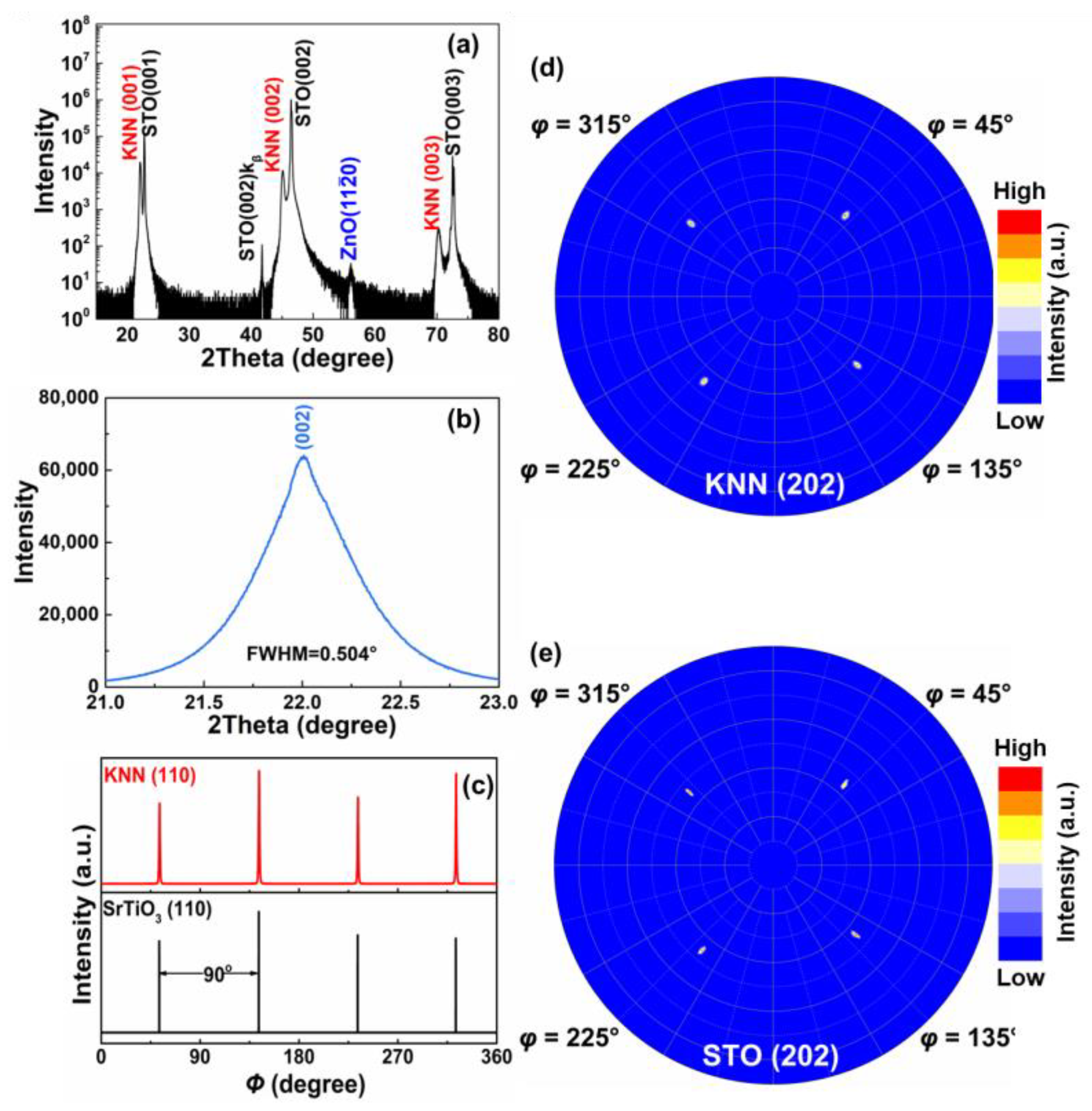
The crystalline phase of the KNN-ZnO composite films was studied using XRD patterns.
Figure 1a shows the
θ–2
θ XRD patterns of KNN-ZnO composite thin films in a 2
θ range from 15° to 80°. It can be seen that the highly textured KNN phase and non-ferroelectric ZnO phase have grown on the (001) STO substrates. The preferentially [001]-orientated KNN phase was observed. The minor peak near the angle of 56.5° belongs to the non-ferroelectric ZnO (11
0) peak. No other phases were detected in the
θ–2
θ XRD patterns in addition to the diffraction peaks belonging to the KNN-ZnO composite films and STO substrate. The rocking curve of the (200) peak for the KNN phase demonstrates a low full-width half-maximum (FWHM) of 0.504° in
Figure 1b, indicating a relatively high crystallization of the KNN phase for the KNN-ZnO composite films. The in-plane (IP) relationship of KNN-ZnO nanocomposite films was examined by
φ scan, and the result of the (110) peaks for the KNN phase and STO substrate is presented in
Figure 1c. A 4-fold symmetry characteristic is observed for the KNN phase, similar to the STO substrate, suggesting an OP “cube-on-cube” epitaxy on the (001) STO substrate and two possible in-plane rotations. The 4-fold symmetry cannot be seen for the second phase of ZnO, possibly due to the weak amount of ZnO phase in the composite films.
Figure 1d,e presents the (220)/(202) -pole figures for KNN-ZnO nanocomposite films. After setting the 2
θ at 63.2°, which corresponds to the KNN (220)/(202) reflection, the films were rotated from 0° to 360°. As shown in
Figure 1d,e, four sharp spots of the (220)/(202) reflections were observed at every 90°, and the angle of these spots agreed with those of the STO (202) reflection. This result indicates that the KNN phase in the composite films was grown epitaxially in the out-of-plane direction of the STO substrate and rotated in two possible in-plane directions. Thus, the epitaxy relationships of the film and substrate are determined to be (001)
KNN//(11
0)
ZnO//(001)
STO, [110]
KNN//[0001]
ZnO//[110]
STO and [1
0]
KNN//[0001]
ZnO //[1
0]
STO.
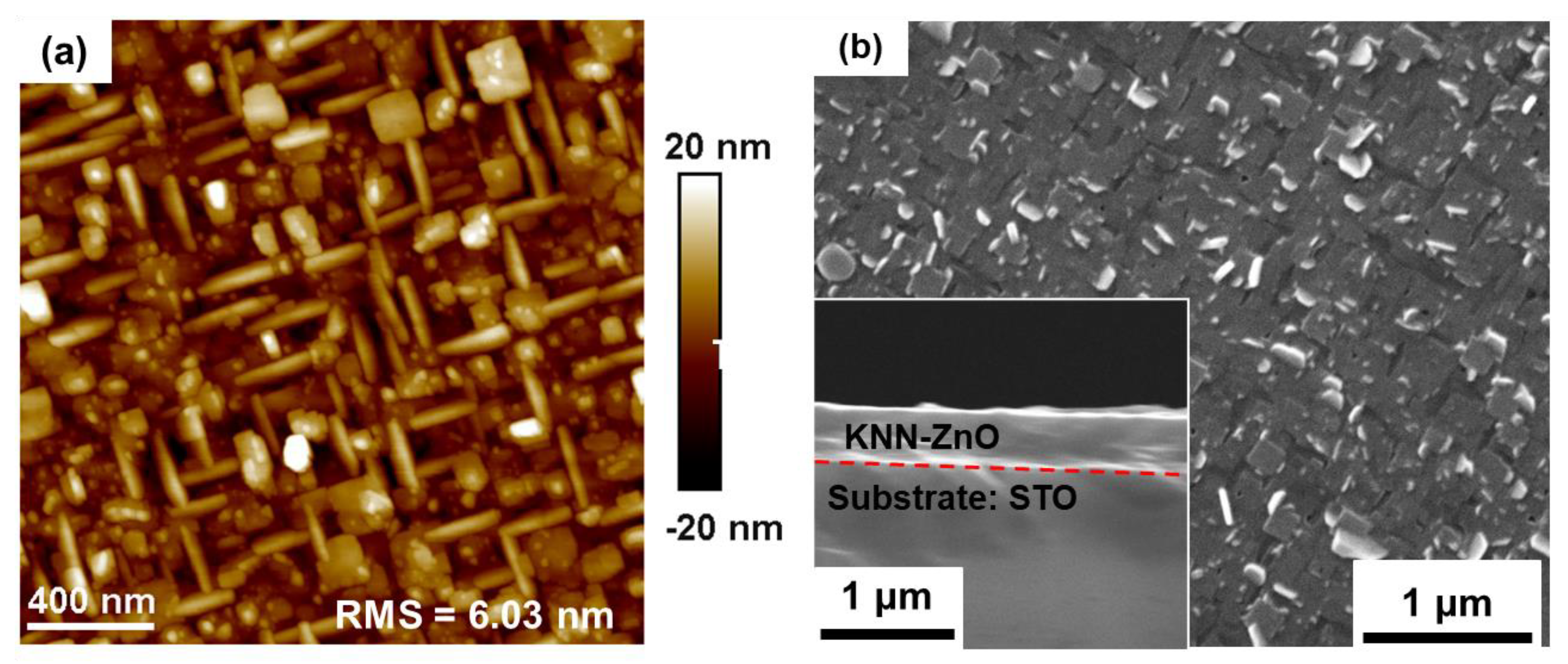
The surface morphologies of the KNN-ZnO composite films are demonstrated by top-view AFM and SEM images, as shown in
Figure 2a,b. It can be seen that the composite films possess two different grain morphologies of “square-like” and “stipe-looking” shapes, which are orderly aligned, as presented in
Figure 2a. Two different kinds of grain sizes of the KNN-ZnO composite films might correspond to two phases, combined with the XRD patterns in
Figure 1a. The films exhibit a smooth surface with a roughness (root mean square, RSM) of 6.03 nm, indicating a smoother surface morphology than films deposited using other methods [
22]. The top-view SEM image of the KNN-ZnO sample (in
Figure 2b) shows a similar tendency to the results presented in
Figure 2a. A dense and smooth surface with square- and stripe-shaped grains is shown in
Figure 2b. The inset in
Figure 2b gives the cross-sectional morphologies of the KNN-ZnO composite films measured by SEM. A dense bilayer structure is composed of the KNN-ZnO composite films and STO substrate. Furthermore, a distinct interface between the film and STO substrate is marked by the red dotted line in
Figure 2b. The thickness of the KNN-ZnO composite film is approximately 360 nm, according to the cross-sectional SEM image.
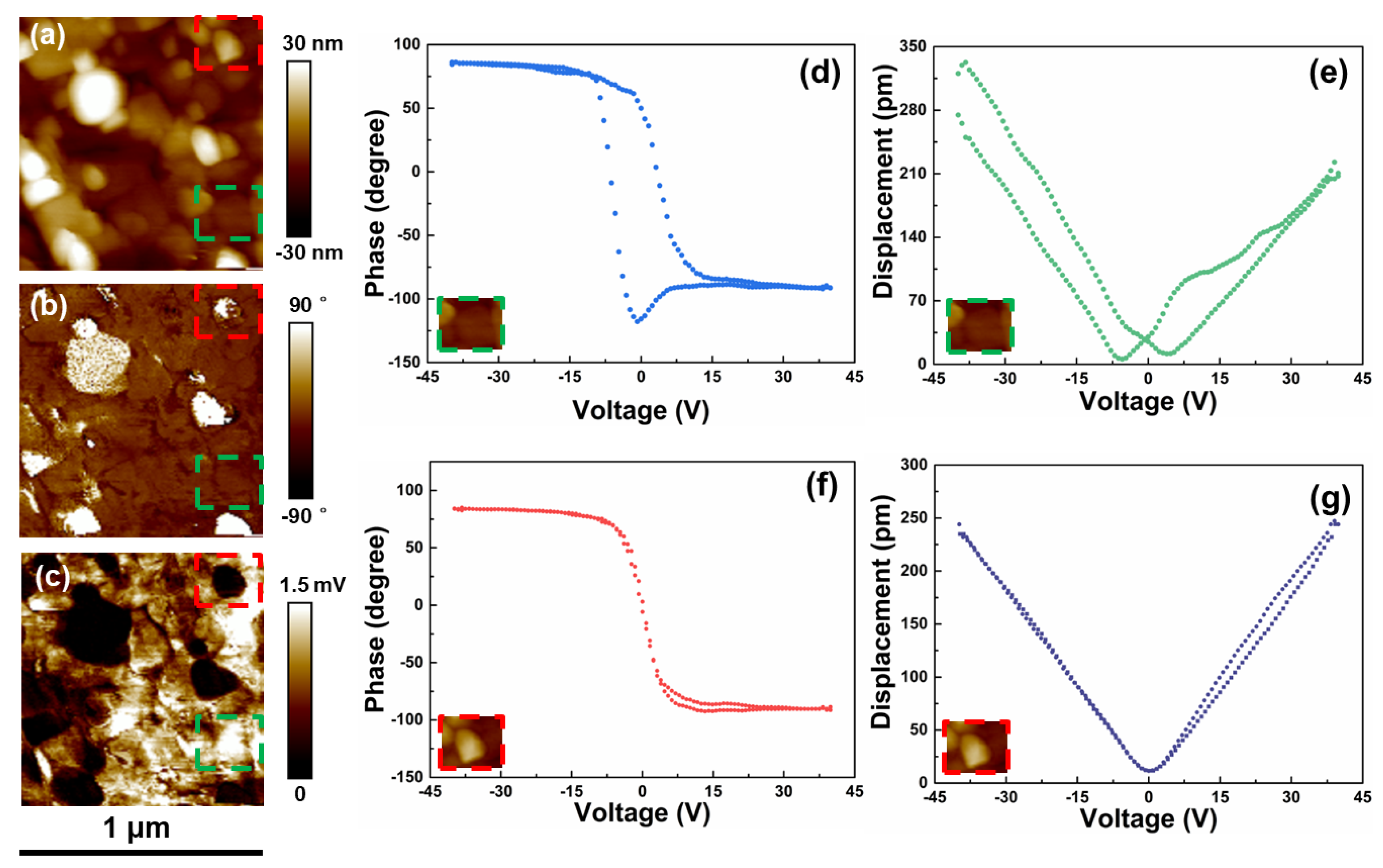
The piezoresponses of the KNN-ZnO composite films were characterized using three-dimensional piezoelectric-response force microscopy (PFM), and the surface topography, local static out-of-plane (OP) phase, and amplitude PFM images are shown in
Figure 3a–c.
Figure 3a shows the surface topography of the KNN-ZnO composite films in a scanned region of 1 μm × 1 μm square area. It can easily be seen that the surface morphology is significantly different from that in
Figure 2a obtained by AFM. The different scan modes and probes are the main reasons.
Figure 3b,c presents the local static OP phase and amplitude PFM images of the films, respectively. The OP PFM phase image exhibits distinct 180° contrast, suggesting different ferroelectric polarization states. The different contrast also appears in the PFM amplitude image, in which the bright and dark areas indicate strong and weak piezoelectric responses, respectively. Upon further inspection, it can be found that two different piezoelectric responses occur among different grains, as indicated by the red and green boxes. According to the XRD, AFM, and SEM results, the KNN and ZnO phases are grown along specific directions on the STO substrate and are orderly arranged. ZnO has a weak piezoelectric property and is usually used as a transparent conductive material in ultraviolet regions. Therefore, it is hard to obtain the phase and amplitude signals using PFM for the ZnO phase. As a result, it could be concluded that the strong and weak piezoresponse areas are the KNN and ZnO phases, respectively. To further make a distinction between KNN and ZnO phases, the dynamic OP piezoelectric phase hysteresis loops and displacement-voltage butterfly loops were acquired in vertical PFM mode, in which the tip was fixed on the surface of the film while applying a direct current (DC) bias from −40 V to +40 V. It is noted that the piezoresponses of the thin films are intensely dependent on the measurement conditions, such as the types of probes, the locations of the laser, and the contact area of the probes and film surface [
22]. Therefore, the PFM measurements of the different grains for the KNN and ZnO phases were detected under similar conditions, aiming to ensure the reliability and authenticity of the PFM data. The different grains marked by red and green boxes were chosen as measured film surfaces, and the results are shown in
Figure 3d–g.
Figure 3d,e shows an OP PFM phase-voltage hysteresis loop and a displacement-voltage butterfly loop for the dark grain (marked in the green box), respectively. The phase hysteresis loop manifests an almost symmetric “square” shape, as shown in
Figure 3d. Meanwhile, the displacement loop in
Figure 3e shows a typical “butterfly” loop with a significant hysteresis. This means that the dark grain marked by the green box possesses a high OP polarization, indicating a typical piezoelectric nature. In contrast, as shown in
Figure 3f,g, the bright grain, which is marked by the red box, exhibits a closed phase hysteresis loop and a tight displacement-voltage loop, reflecting a lower OP polarization. This phenomenon might be related to the electrostatic effect that occurred during the PFM measurement processing. In addition, the OP phase-voltage hysteresis loops and displacement-voltage butterfly loops were characterized by the two types of grains under the same conditions, as shown in
Figure 3d–g. The electrostatic effect is not the main reason for the closed phase-voltage hysteresis loop and displacement-voltage butterfly loop marked by the red box. These results also support the conclusion obtained in local static OP PFM phase and amplitude analysis, in which the strong and weak piezoresponse grains correspond to the KNN and ZnO phases, combined with the XRD patterns in
Figure 1a and surface morphologies in
Figure 2a.
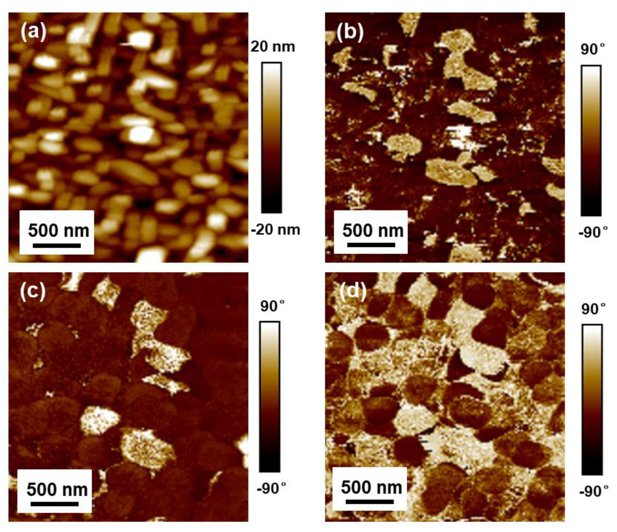
The domain evolutions of the KNN-ZnO composite thin films measured under different DC biases are displayed in
Figure 4. It was found that the domains cannot be completely switched, even under a high DC bias of ±50 V superimposed on an AC modulation bias (
f = 45 kHz,
Vpp = 5V).
Figure 4a–d gives the surface image and phase images under different DC bias voltages of 0, 50 V, and −50 V for the KNN-ZnO composite films. Two different OP phase components are exhibited in the KNN-ZnO composite films; dark and bright regions represent KNN and ZnO phases, respectively, as shown in
Figure 3b and
Figure 4b. An obvious difference can be noticed in the OP phase images of the films under positive and negative DC bias. Under the positive DC bias, some dark areas are switched to the opposite state, whereas some bright areas are not changed, as shown in
Figure 4c. Under the negative DC bias, the original dark PFM phase is turned to the opposite orientation, whereas the bright area remains stable, as shown in
Figure 4d. This indicates that the two different polarization behaviors obtained under DC bias belong to two phases. Similarly to the area marked by the red dotted line, the grains cannot be switched under both positive and negative DC biases of ±50 V. Combined with the analysis mentioned above, the stable domains could correspond to the ZnO phase, whereas the switched area should be related to the KNN phase, respectively.
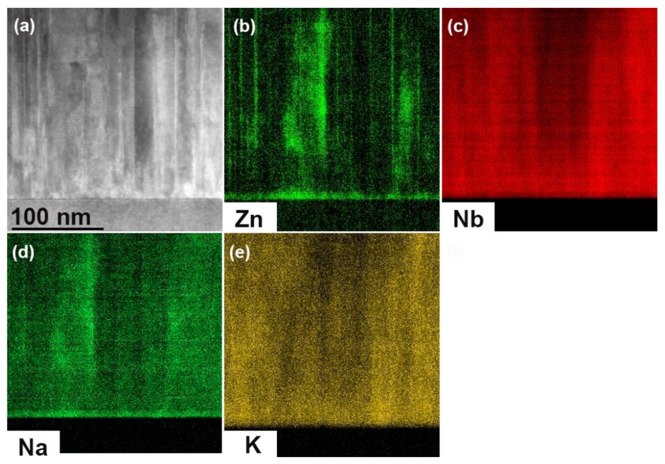
The systematic variations in the KNN-ZnO composite thin films strain are most likely related to the microstructure. Further microstructure characterization and phase structure identification of the KNN-ZnO composite thin films was performed using a low-resolution scanning transmission electron microscope (STEM). The detailed cross-sectional image is shown in
Figure 5a to reveal the interface structure of the KNN-ZnO composite thin films. A distinct interface between the KNN-ZnO films and STO substrate was observed. Many vertical nanocolumns (in bright contrast) are distributed in KNN-ZnO composite film matrix (in dark contrast) and extend perpendicular to the (001) STO substrate. This kind of nanostructure with a uniform diameter of approximately 1–2 nm is randomly obtained throughout the entire thickness of the films, forming the chessboard-like topography surface, as shown in
Figure 2a,b. For the KNN-ZnO composite thin films, the KNN and ZnO phases have grown alternately and vertically aligned on the STO substrate, indicating that the samples are self-assembled. The vertical arrangement in the KNN-ZnO composite thin films is further investigated using energy-dispersive X-ray spectroscopy (EDS) technology.
Figure 5b–e displays the EDS elemental mappings of Zn, Nb, Na, and K elements in the KNN-ZnO composite films, respectively. It can be seen that there is a distinct phase separation between the nanocolumns and film matrix, and the chemical composition of the nanocolumns mainly consists of Zn elements with small amounts of K, Na, and Nb. The EDS mapping analysis suggests that a vertically aligned nanostructure as the ZnO phase is embedded in the KNN phase matrix along the (00l) orientation. Such an alternate structure assured sufficient vertical interface between the KNN phase and ZnO phase, enabling the strain control of the KNN phase from the ZnO phase. In addition, this indicates that the ZnO component contributed to the formation of nanocolumns and the introduction of vertical heteroepitaxial strain.
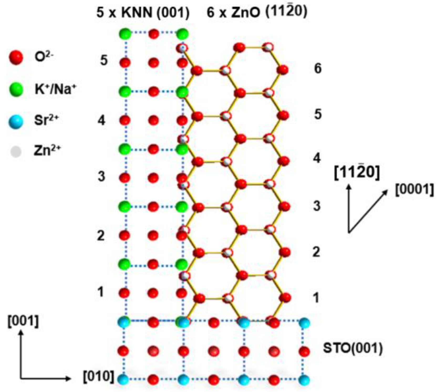
As mentioned above, the KNN and ZnO phases are alternately arranged and vertically grown on the (001) STO substrate for the formation of the KNN-ZnO composite films. According to the XRD results, the epitaxy relationships of the KNN phase, ZnO phase, and STO substrate were determined to be (001)
KNN//(11
0)
ZnO//(001)
STO, [110]
KNN//[0001]
ZnO//[110]
STO and [1
0]
KNN//[0001]
ZnO//[1
0]
STO. Furthermore, the lattice parameters of the KNN phase and ZnO phase were calculated using Bragg’s equation (2
dsin
θ = n
λ) to be 3.992 Å and 3.258 Å [
36]. The KNN lattice matches well with the STO substrate (
aSTO = 3.905 Å), whereas the ZnO phase presents a large mismatch with both KNN and STO. Due to the formation of nanocolumns in the vertically epitaxial KNN-ZnO composite films, the crystallographic schematic diagram of the vertical interface could be described, as shown in
Figure 6. The ratio of the KNN phase and ZnO phase along the (001) direction was determined to be 5: 6, favoring a vertical cube-on-cube growth despite the large lattice mismatch. The origin of the vertical strain is also correlated with the out-of-plane lattice mismatch between the KNN and ZnO phases.
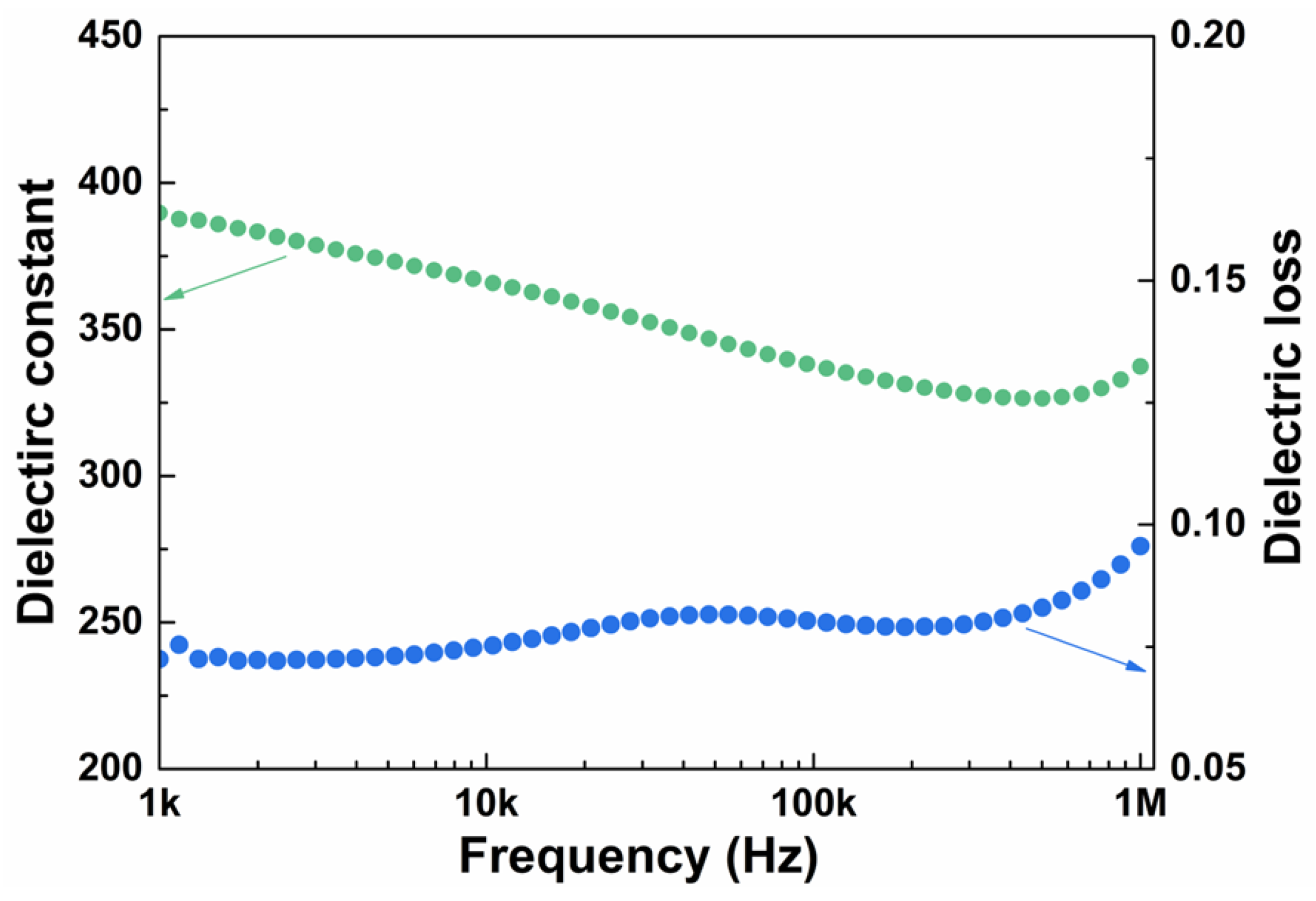
The frequency dependence of the dielectric constant and dielectric loss of the KNN-ZnO composite films is illustrated in
Figure 7. As the frequency increases from 1 kHz to 1 MHz, the dielectric constant of the KNN-ZnO composite films gradually decreases, whereas the dielectric loss continuously increases, which is a common feature for the perovskite structure materials [
16,
22]. It can also be seen that the KNN-ZnO composite films show the largest constant of ~390 and the lowest dielectric loss of ~ 0.07 at a frequency of 1 kHz. The value measured at room temperature is similar to that of single-phase KNN thin films reported in the previous literature [
16,
37]. This result indicates that vertical strain control is a useful method to improve the electrical properties of vertically epitaxial KNN-ZnO composite thin films.


