1. Introduction
The lower-cost Czochralski single-crystal silicon (CZ-Si) growth method is still the main semiconductor manufacturing process. In addition, CZ wafers can be p-type or n-type, whereas wafers made from multi-crystalline silicon methods are mostly p-type [
1]. Yet, multi-crystalline silicon wafers have been gradually replaced now by monocrystalline Cz-Si wafers [
2,
3,
4]. However, in the process of growing single-crystal silicon, the heat flow field distribution [
5,
6], oxygen-related defects [
7,
8,
9], and intrinsic defects [
10,
11,
12] of the crystal will affect the quality of single-crystal Si. Therefore, finding suitable growth conditions is necessary for the development of high-quality single-crystal silicon.
The CZ method was invented by J. Czochralski [
13] in 1917 to grow semiconductor crystals. At that time, effort was mainly focused on the solid–liquid interface solidification rate. In 1950, Teal et al. [
14] doped Ge into single-crystal silicon, which laid an important cornerstone for later silicon single-crystal growth technology. In 1982, Voronkov et al. [
15] researched and put forward the pulling rate (
V)/temperature gradient (
G) theory, discussing that the defect types inside the crystal rods correspond to the specific relationship between
V and
G. In 1983, Hurle et al. [
16] used the Laplace–Young equation to calculate the relationship between the solid, liquid, and gas interface angles based on the capillary phenomenon. In 1986, Derby and Brown [
17,
18] simulated the relationships between the heat transfer behavior in the furnace body, the thermal convection of the molten bath, and the shape of the solid–liquid interface by the CZ method. Yi et al. [
19] analyzed the growth process of 6-inch silicon single crystals using the CZ method and discussed the influence of the pulling rate and solid–liquid interface state on the process. In 2001, Takano et al. [
20] discussed the correlation between the design of the furnace body and ingot size, comparing the thermal field of large- and small-size crystal growth. In 2008, Jing et al. [
21] described the factors affecting the convection of the molten silicon, including natural convection, forced convection caused by crystal rotation, crucible rotation, and surface tension flow. The crystal rotating rate will change the shape of the solid–liquid interface, and the type of interface will change the flow field of the molten silicon. In 2012, Chen et al. [
22] used CGSim to conduct dynamic simulations for CZ crystal growth. The tuning factors included the change of oxygen concentration and the flow distribution of the molten silicon and gas. In 2018, Zheng et al. [
23] constructed a first-principle model, which consisted of energy, mass balance, hydrodynamic, and geometrical equations to calculate the crystal radius and the crystal growth rate as output variables by using the heater input, crystal pulling rate, and crucible rise rate as input variables. In 2021, Kato et al. [
24] modified the first-principle model of Zheng et al. with higher accuracy, realizing model predictive control of the CZ process.
It is known that p-type Cz-grown silicon has defects, such as B-O (based on doping concentrations) defects and metallic (Fe and Cr) contamination, which can be the reason behind the lifetime of the samples, resulting in the degradation of device performance. Nonetheless, n-type monocrystalline Cz-grown silicon does not contain boron, so it is unaffected by B-O defects or iron-boron (Fe-B) pairing reactions. However, intrinsic and micro-defects, such as flow pattern defects (FPDs), as well as oxygen induced stacking faults (OISF), are commonly associated with n-type Cz-grown silicon, which degrades the device performance. There are two types of micro-defects during the production of single-crystal silicon wafers, A-defect and D-defect. They are agglomerations of intrinsic point defects. The first type are A-defects, which are silicon self-interstitials. When the silicon self-interstitials concentration is higher than the supersaturation, it will coalesce into A-swirls. On the contrary, they coalesce into smaller micro-defects, B-swirls, when the silicon self-interstitials concentration is lower than the supersaturation [
25]. Generally, the cutting of the wafer is perpendicular to the growth axis. As the cross-section of the wafer is not the solidification track during growth, the solid–liquid interface in the crystal growth state is concave or convex. Therefore, the crystal state can be observed by the resistance distribution of the doped crystal. Additionally, oxygen, impurities, and irregular turbulence will cause swirl defects [
26] during the rotation of the silicon ingot. The second type of defect is the D-defect [
27], which is agglomerated collectively by silicon vacancy. According to different detection methods, D-defects have different names, such as flow pattern defects (FPDs), crystal-originated particles, and light-scattering tomography defects. Warangkula [
28] discussed and conducted etched tests on FPDs. The density of FPDs will directly affect gate oxide reliability.
However, when silicon crystals are exposed to high-temperature wet oxidation at 900 °C to 1200 °C, oxidation-induced stacking faults (OISFs) form a dumbbell-shaped pattern at the nucleation site. Mechanical damage and thermal oxidation treatment may also cause OISFs. Generally, OISFs are found at the junction of the vacancy/interstitial boundary, with an appearance of a ring-shaped distribution. By changing the crystal growth and adjusting the thermal cycle conditions, OISF defects could be effectively avoided. Hasebe et al. [
29] found that as the pulling rate increases, the OISF ring will move to the edge of the ingot, and then the center of the ingot is occupied by vacancies. Conversely, when the pulling speed decreases, the OISF ring will move to the center of the ingot and the surroundings of the ingot will be concentrated by silicon self-interstitials. In 2002, Okui and Nishimoto [
30] researched the relationship among the OISF ring, pulling rate, and temperature gradient, showing that the temperature gradient of the ingot will influence the type of defect generation.
There are many defects in silicon wafers, which have led to a decline in component yields and wafer thinning to reduce costs. As the thickness of the substrate decreases, the recombination rate decreases, thus magnifying the effect of defects [
31]. Although simulation models use
V/
G theory to predict crystal growth conditions, it is difficult to detect the temperature gradient during the process of pulling the ingot. Since crystallographic defects in silicon are mobile at high temperatures, their density and distribution are regarded as technically relevant, which can affect the performance of electronic devices [
32]. Therefore, this work elucidates the ideal growth parameters, such as furnace pressure, crucible rotation, and interstitial oxygen (
Oi) concentration and pulling rate using the CZ method, to reduce micro-defects in order to enhance device performance.
2. Materials and Methods
The CZ method involves putting a small seed crystal into the crucible and melting it by either resistance or radio-frequency heaters. Typically, a seed crystal with a diameter of a few millimeters is dipped from the top into the free melt surface, and a small portion of it melts. The contact interface between the seed and the melt results in the formation of a melt meniscus. A new crystal portion is formed at the interface as the seed is slowly pulled from the melt (often under rotation), as shown in
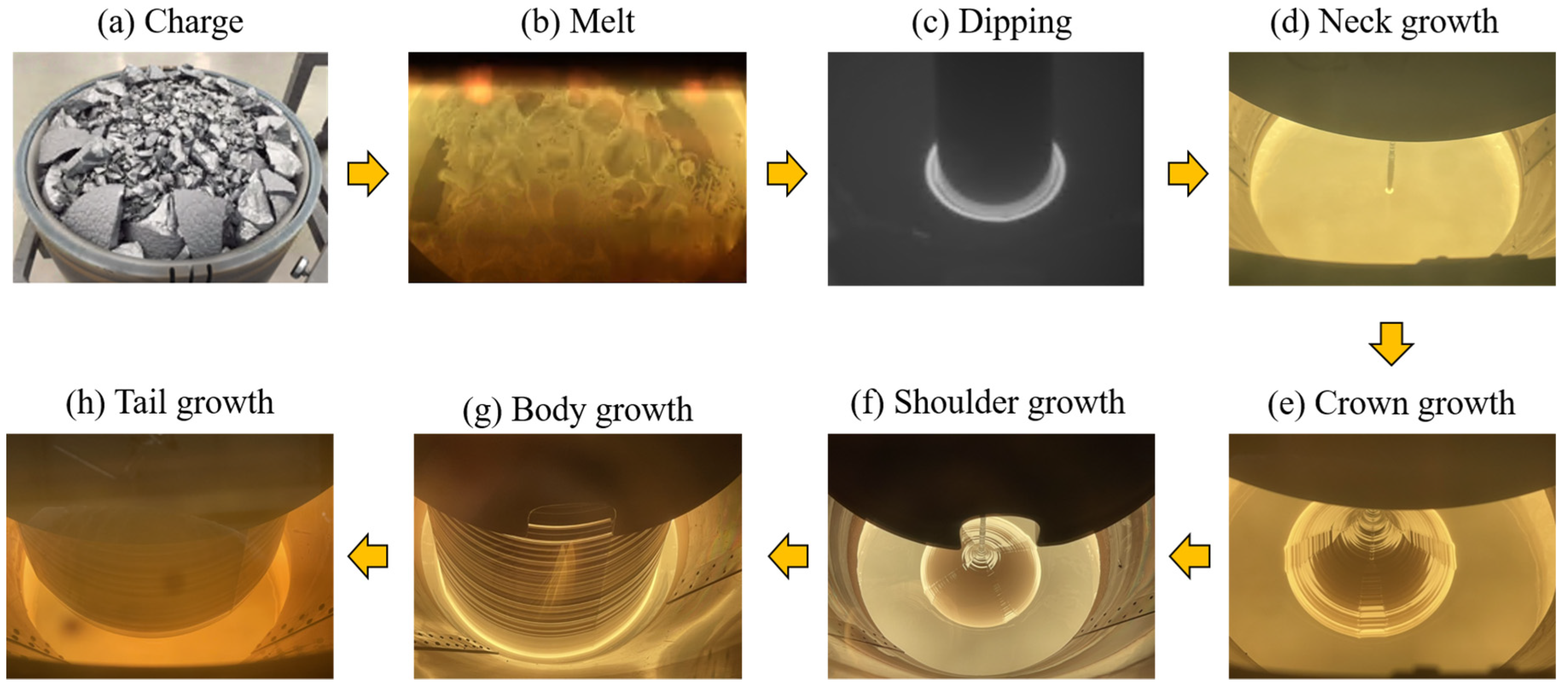
Figure S1. The single-crystal growth by Czochralski furnace (PVA TePla, Wettenberg, Germany), a filler with a 190 kg boron-doped p-type single-crystal silicon ingot in the [100] direction, and the resistivity was set to ~10–15 Ω-cm; the wafer growth size was 12 inches. The process of the CZ-Si growth furnace was followed as (a) charge, (b) melt, (c) dipping, (d) neck growth, (e) crown growth, (f) shoulder growth, (g) body growth, and (h) tail growth, as shown in
Figure 1. To increase the stability of the process, the speed of ingot rotation and the initial position of the crucible were fixed. Crucible rotation and furnace pressure were more influential factors, providing different initial oxygen concentrations.
The samples were acquired from the ingot head, as shown in
Figure 2. The wafer thickness was 2.5 ± 0.5 mm, perpendicular to the [100] crystal orientation, and sliced into a ¼-size fan-shaped sample, as shown in
Figure 2. According to
Figure 2, the radial distribution of 5 ± 5, 60 ± 5, and 120 ± 5 mm is defined as Center, R/2, and Outer, respectively.
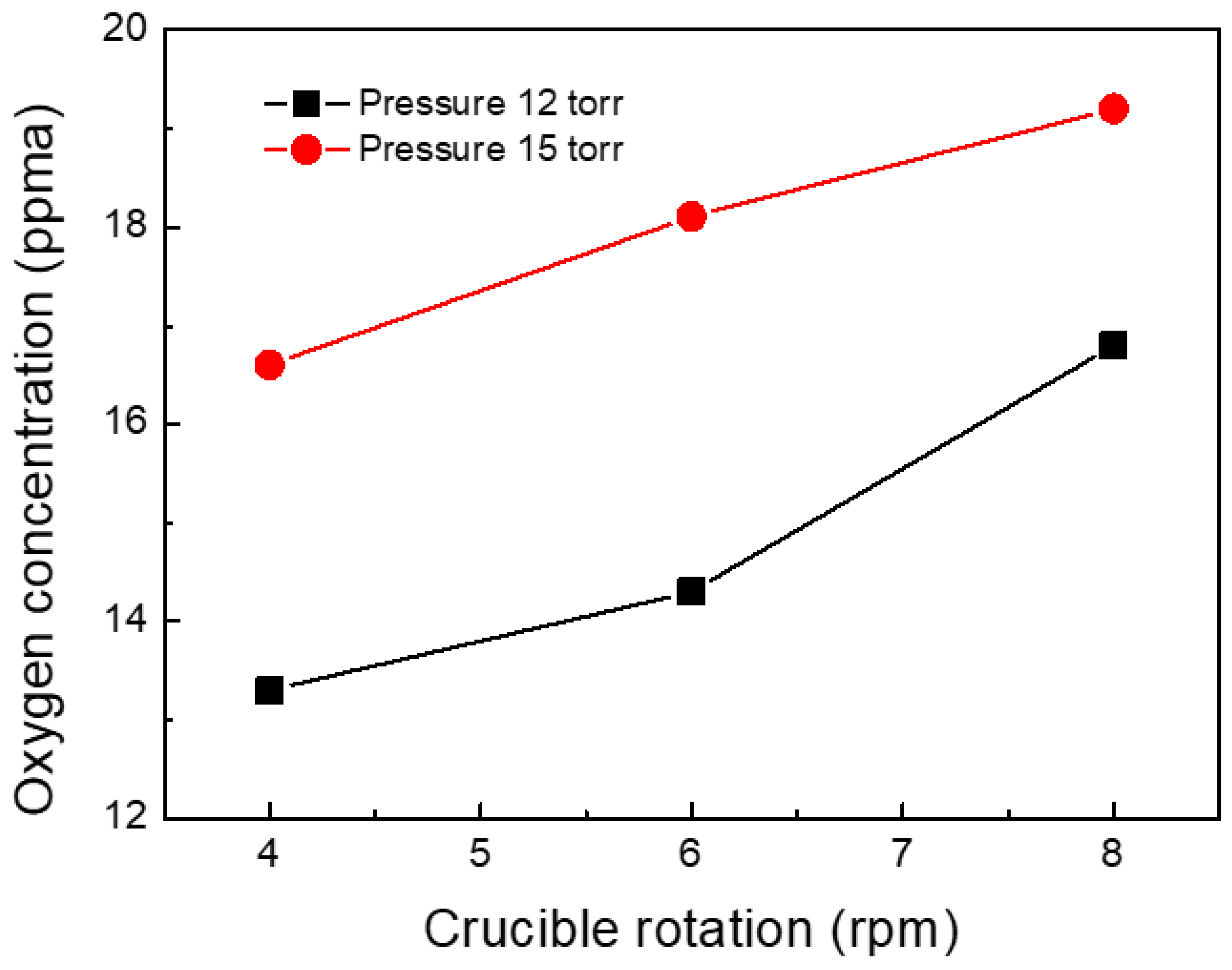
Figure 3 shows the relationship among the
Oi, the furnace pressure, and the crucible rotation. The
Oi content has a positive correlation with furnace pressure and crucible rotation.
V/
G theory is defined by the intrinsic point defects affected by the pulling rate and the temperature gradient in the silicon single-crystal growth process. In this study, samples A, B, C, D, and E were cut out from the ingot, which has different growing conditions during the process of the CZ-Si growth furnace, as listed in
Table 1. The pressures, rotation speeds, and pulling rates would affect the
Oi of the Czochralski single-crystal silicon ingot. Yet, the pulling rate not only affects the
Oi, but also a radius of an ingot, which would affect the result of the average radial distribution defect density. Therefore, we take
Oi as the result of the variables for the pressures and rotation speeds and extract the pulling rate out.
For observing the FPDs and OISFs, the experimental process had six main steps: (1) silicon ingot growth and sample collection; (2) etching and polishing; (3) Secco etching and FPDs observation; (4) carrier lifetime measurement and analysis; (5) a high-temperature wet-oxidation MAE2 etching and OSIF observation, whereby the MAE2 was prepared with a volume ratio of 1:1:3 for HF (49%), HNO3 (49%), and CH3COOH (95%); and (6) carrier lifetime measurement and analysis. Since the parameter settings during crystal growth will affect the change of oxygen content and fluid convection, the CZ method was used to tune the optimum parameters.
To observe the FPDs, the samples were immersed in a 30 °C MAE1 for surface polishing. MAE1 consists of HF (49%), nitric acid (HNO
3, 49%), and acetic acid (CH
3COOH, 95%) in a volume ratio of 1:1:2. The etching time was 5 min, and the solution etching rate was about 0.14 mm/min; photographs of the process are shown in
Figure S2a. To observe the impact of FPDs caused by the pulling rate on carrier lifetime, we used the etching process. Firstly, the polished sample was placed in an SC1 solution with an ultrasonic vibrator to remove dirt and particles, as shown in
Figure S2b. SC1 is a mixture of 5% H
2O
2 and 1% NH
4OH. Second, to observe the FPDs, samples were vertically immersed in the Secco solution and statically left for 30 min. Secco is a mixture of 49% HF and 0.15 M K
2Cr
2O
7 solution in a volume ratio of 2:1. The silicon wafer reacted with the Secco solution, generating hydrogen bubbles that adhered to the surface of the samples and then left a V-shaped etching pit behind. Third, the surface of the samples was cleaned for a second time, as described in the first step. After completion, an optical microscope (OM) was used to record the number of FPDs and the microwave photoconductive decay (
µ-PCD) to measure the impact of the defects on carrier lifetime. For inducing OISFs, the heating parameters of the high-temperature annealing furnace are shown in
Table S1. The detailed process steps are as follows. (1) The sample was sent into a high-temperature furnace and heated from room temperature to 400 °C. (2) The temperature of 400 °C was maintained for 5 min. (3) The sample was heated with a heating rate of 8 K/min to 800 °C. Simultaneously, the dry oxygen process started at this step, and the oxygen flow rate was 2 L/min. (4) The temperature of 800 °C was maintained for 10 min. (5) The sample was heated with a heating rate of 5 K/min to 1100 °C. (6) The 1100 °C temperature was maintained for 60 min. Simultaneously, the wet oxygen process began at this step. (7) After 60 min, the wet oxygen process was terminated. The sample was cooled with a cooling rate of −3 K/min to 800 °C. Simultaneously, the dry oxygen process started again, and the oxygen flow rate was 2 L/min. (8) After the above stages were completed, the dry oxygen process ended, and the sample was cooled down by furnace cooling.
After completion, a blue-green oxide layer was observed on the surface, and the samples were then immersed in the MAE2 mixed solution for 2 h for surface polishing. The mixed solution was prepared with a volume ratio of 1:1:3 for HF (49%), HNO
3 (49%), and CH
3COOH (95%). After the above process was completed, samples were rinsed with deionized water and blown dry, as shown in
Figure S2c. Finally, an OM was used to record the number of OISFs. The reader is encouraged to go through the references [
33,
34,
35] to know the details about the various kinds of etching used in this study, such as MAE1, MAE2, SC1, and Secco. The
µ-PCD was used to measure the impact of the defects and the difference of
Oi (delta
Oi) on the carrier lifetime. The delta
Oi is from the Fourier-transform infrared spectroscopy (FTIR) measurements before and after a high-temperature wet oxidation. The following reagents were used in this work—Hydrofluoric acid (HF): ACS reagent, ≥48% (Sigma-Aldrich, St. Louis, MO, USA); Potassium dichromate (K
2Cr
2O
7): ACS reagent, ≥99.5% purit (Sigma-Aldrich, St. Louis, MO, USA); Hydrogen peroxide (H
2O
2): ≥35% purity (Sigma-Aldrich, St. Louis, MO, USA); Nitric acid (HNO
3): ≥99% purity (Sigma-Aldrich, St. Louis, MO, USA); Acetic acid: ≥99% purity (Sigma-Aldrich, St. Louis, MO, USA); and Ammonium hydroxide (NH
4OH): ≥99% purity (Sigma-Aldrich, St. Louis, MO, USA).
3. Results and Discussion
The number of FPDs is counted from the OM image, as shown in
Figure S3. The FPDs with radial distribution have no obvious regularity for each sample, which is presumed to be the influence of the change of the crucible rotation and the convection of the melting heat during the crystal growth process. The density for the radial distribution of the FPDs shows an inverse tendency with a radius for samples A, B, and C, while this is not obvious for samples D and E, as listed in
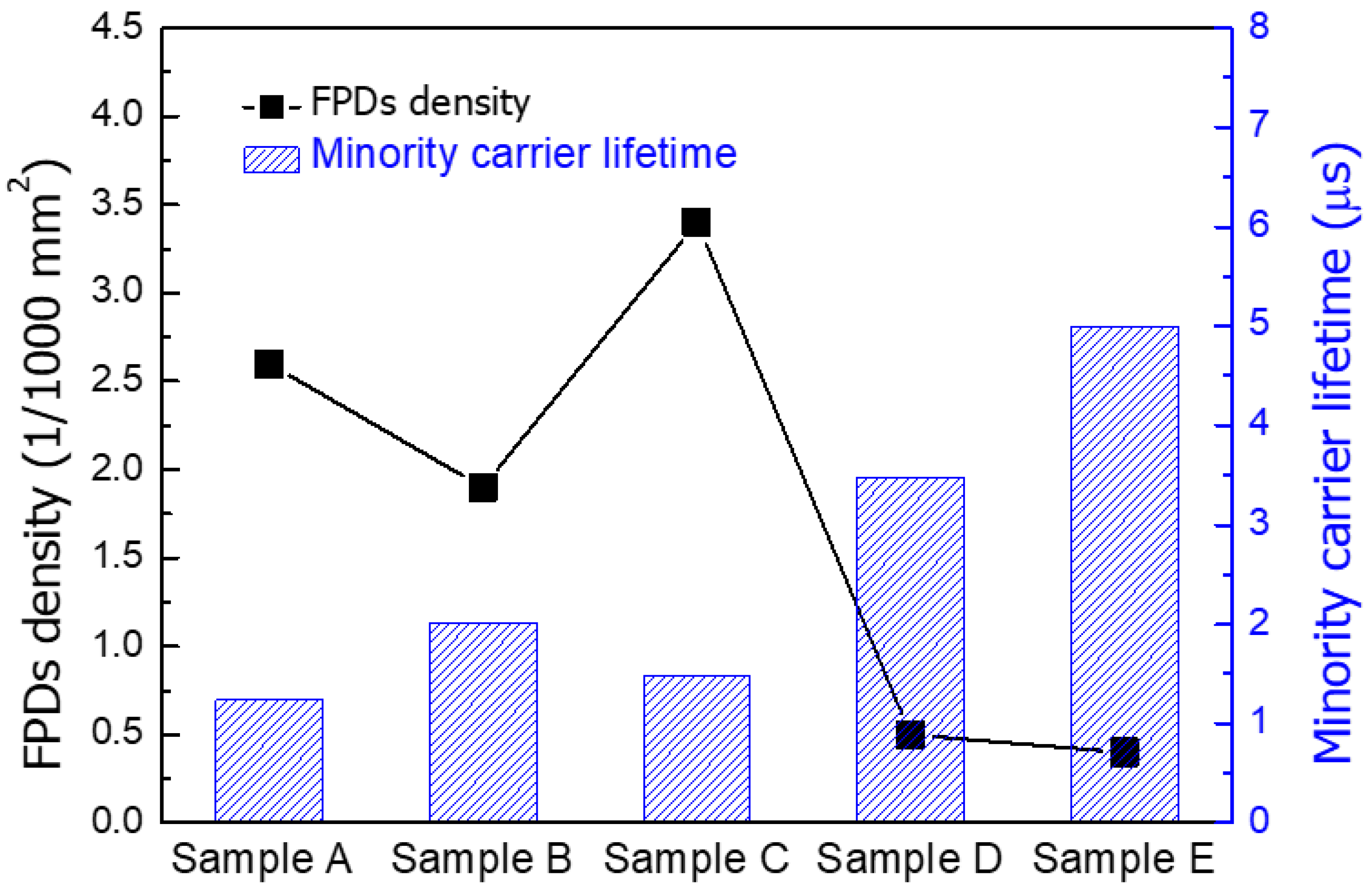
Table 2. Moreover, according to the data of the average radial distribution defect density, the FPDs per unit area with high pulling rate (samples A = 2.6, B = 1.9, and C = 3.4 1/1000 mm
2) are higher than those with the low pulling rate (samples D = 0.5 and E = 0.4 1/1000 mm
2) by approximately five to eight times. Samples A, B, and C have a relatively high number of FPDs, with a pulling rate of about 0.75 mm/min, whereas samples D and E have relatively few FPDs, with a pulling rate of about 0.35 mm/min. The data show that the FPDs and pulling rate are positively correlated.
The sample was then placed into the
µ-PCD for minority carrier lifetime measurements, and the relationship between the average lifetime and the number of FPDs was compared, as shown in
Figure 4. High-density FPDs have a lower carrier lifetime, whereas low-density FPDs do not. The high pulling rate contains more FPDs, which will affect the recombination of electrons and holes, decreasing the carrier lifetime. Samples B and D have the same
Oi concentration, but different pulling rates, which makes the number of FPDs per area drop from 1.9 to 0.5 1/1000 mm
2, and the carrier lifetime increase from 2.02 to 3.48 µs. Samples C and E have the same smaller
Oi concentration, but different pulling rates, which makes the number of FPDs per area drop from 3.4 to 0.4 1/1000 mm
2 and the carrier lifetime increase from 1.48 to 4.99 µs. However, with the same pulling rate, samples A, B, and C have different
Oi concentrations, and for each sample, the number of FPDs per area is 2.6, 1.9, and 3.4 1/1000 mm
2, respectively, and the minority carrier lifetimes are 1.24, 2.02, and 1.48 µs, respectively. Similarly, samples D and E have no obvious trend between
Oi concentration and FPD; the number of FPDs per area is 0.5 and 0.4 1/1000 mm
2, respectively, and the minority carrier lifetimes are 3.48 and 4.99 µs, respectively. From the above results, the impact caused by the pulling rate on FPDs is greater than that caused by the
Oi concentration.
Generally, an appropriate amount of oxygen precipitates will inhibit dislocation generation and slide to improve the mechanical properties of silicon crystals. However, if they exist in the device, they may affect the conductivity and current leakage around a PN junction. Therefore, for revealing OISFs, the silicon wafer was subjected to a high-temperature wet oxidation and then etched in MAE2. The OISF defects were photographed by OM with an objective lens (10× magnification). After the silicon wafer was passed through a high-temperature wet oxidation, the statistical results show that samples A, B, and D, with
Oi concentrations of over 16.5 ppma, have significantly more (~10–26 times) OISFs than samples C and E have, as listed in
Table 3. With increasing ingot length and decreasing temperature, the radial distribution of oxygen precipitates, which is closely related to the distribution of vacancies and interstitial atoms, is not uniform. For samples A, B, and D, the radial distribution of the high
Oi shows that the center density of OISFs is higher than the surrounding area, as listed in
Table 3. On the contrary, for samples C and E, the low
Oi shows the reverse.
Figure S4 shows the surface morphology results, which are distinguished by Center, R/2, and Outer. The observed OISFs are all parallel or perpendicular to each other in rod-like or half-moon-shaped patterns, owing to the OISFs, and (100) intersecting the <110> direction. According to the results, the density of the OISFs is A > B ≥ D > C ≥ E. The
Oi concentration and the density of the OISFs are positively correlated.
Figure 5 shows the relationship between the delta
Oi and the radial distribution of the OISFs. After a high-temperature wet oxidation, sample A (initial
Oi of 19 ppma), samples B and D (initial
Oi of 16.5 ppma), and samples C and E (initial
Oi of 13.5 ppma) showed
Oi decreases of 65%, 15–25%, and 2–6%, as shown in
Figure 5a–e, respectively. The radial distribution of the delta
Oi shows a reverse correlation with radius growth.
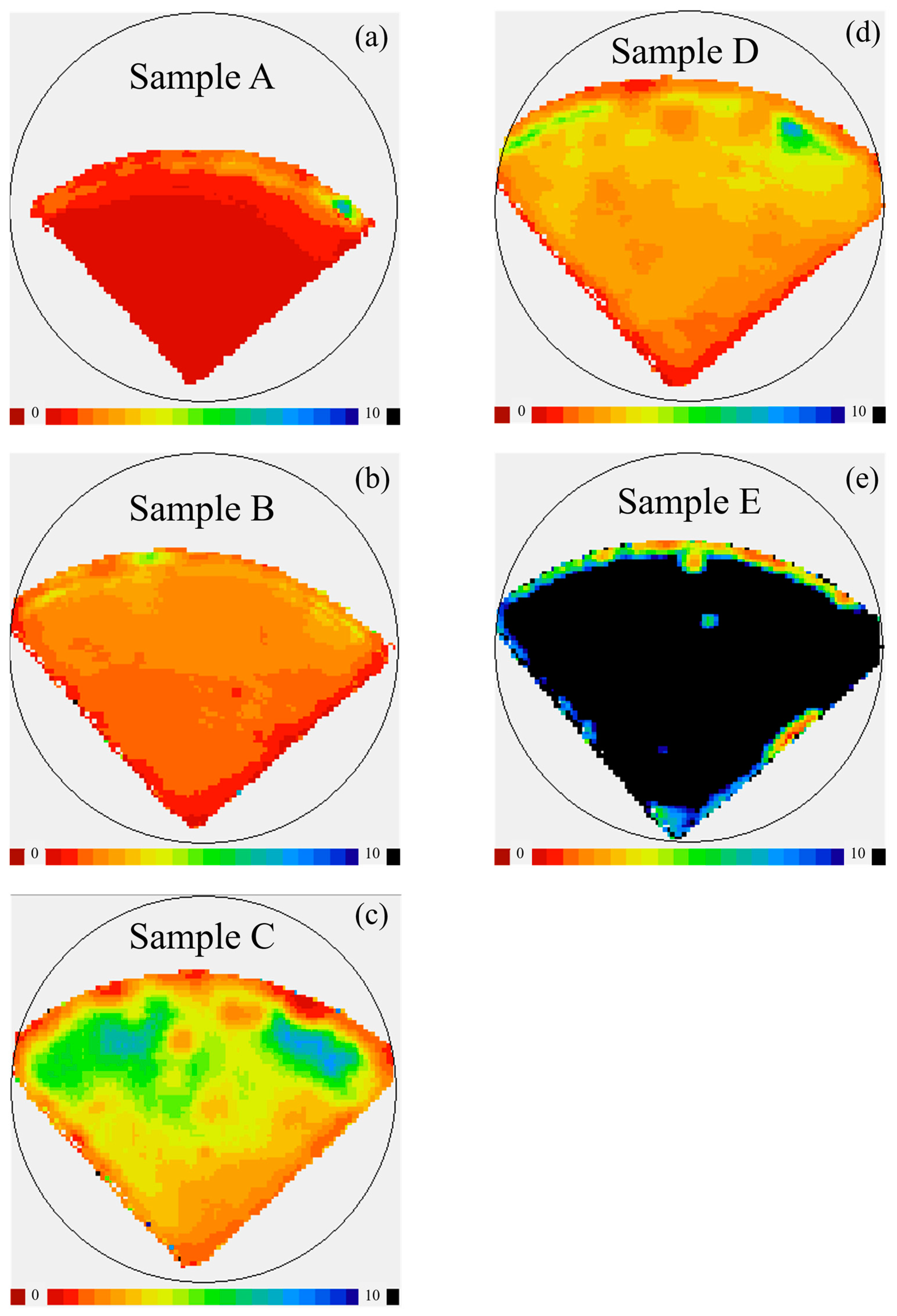
The samples were put into the
µ-PCD for mapping the minority carrier lifetimes of sample A, B, C, D, and E, as shown in
Figure 6a–e, respectively. The color from red to black indicates the minority carrier lifetime from low to high, respectively. The radial distribution of minority carrier lifetimes shows an inverse tendency compared to the difference in oxygen concentration (delta
Oi) from
Figure 5, which is in good agreement with R. Basnet’s results [
36].
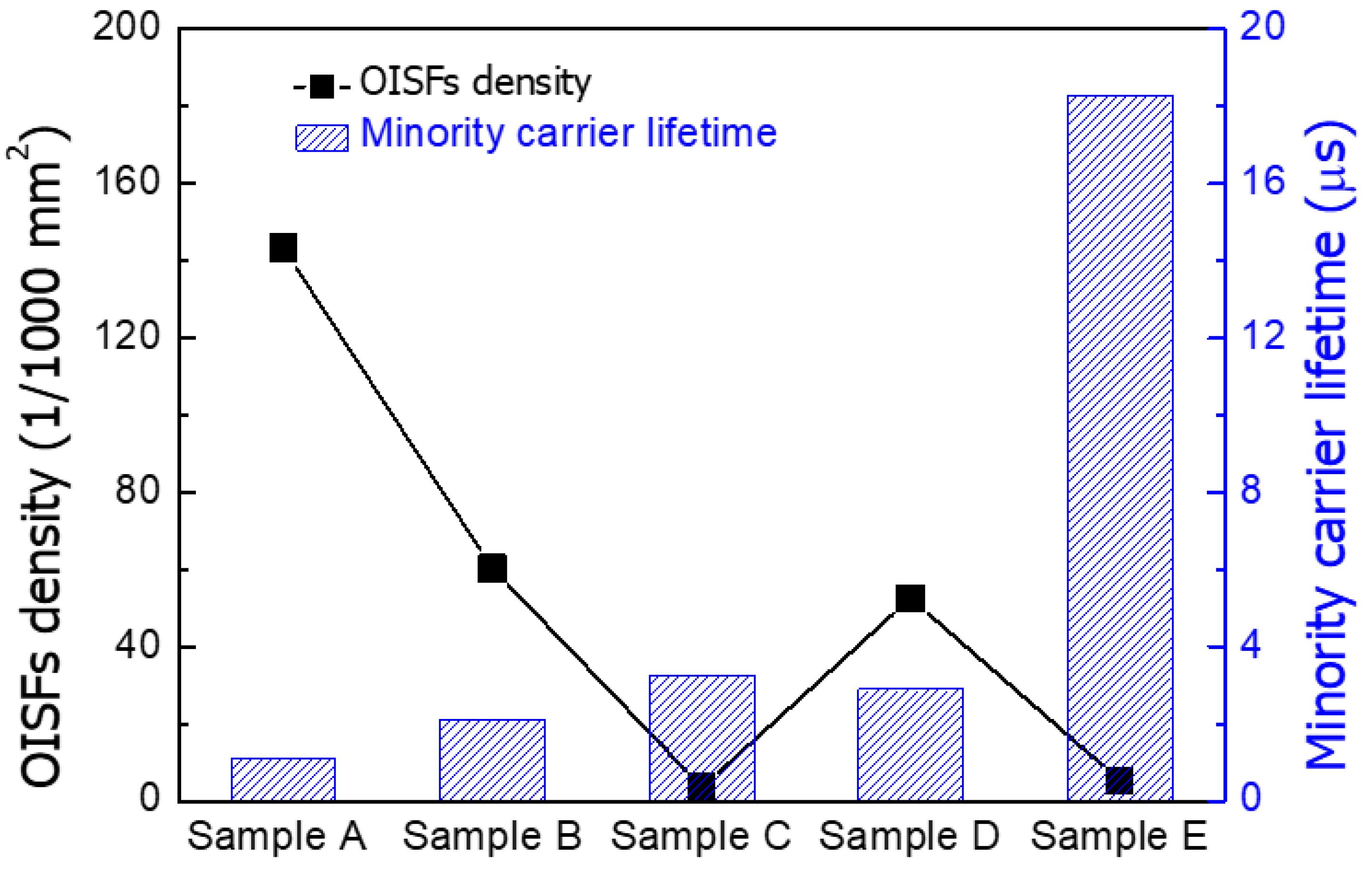
Figure 7 shows the relationship between the average lifetime and the number of OISFs for the samples. For the same pulling rate, high-density OISFs have a lower carrier lifetime, whereas low-density OISFs show the reverse, such as in samples A, B, and C (pulling rate > 0.75 mm/min), and D and E (pulling rate < 0.35 mm/min). On the contrary, for the same
Oi, sample A has the highest initial oxygen concentration of 19 ppma, and its density of OISFs is 143.2 1/1000 mm
2, which has the lowest minority carrier lifetime of 1.1 µs. The
Oi of samples B and D is 16.5 ppma; the number of OISFs is 60.3 and 52.6 1/1000 mm
2, respectively; and the minority carrier lifetimes are 2.12 and 2.9 μs, respectively. The
Oi of samples C and E is 16.5 ppma; the number of OISFs is 3.6 and 5.3 1/1000 mm
2, respectively; and the minority carrier lifetimes are 3.28 and 18.29 μs, respectively. There is no obvious correlation between pulling rate and number of OISFs. Although there is no obvious correlation between pulling rate and OISFs, the pulling rate becomes sensitive to the minority carrier lifetime for low
Oi concentration. Therefore, the minority carrier lifetime of a wafer is dominated by OISFs or FPDs, depending on the
Oi concentration. The results show that sample E has the best growth conditions.
4. Conclusions
In this study, the interstitial oxygen (Oi) concentrations (19, 16.5, and 13.5 ppma) and pulling rates (pulling rate > 0.75 and <0.35 mm/min) on FPD and OISF defects were investigated in detail. The Oi content has a positive correlation with furnace pressure and crucible rotation. For FPD defects, under the same Oi concentrations with various pulling rates, FPDs can be reduced by five to eight times. Simultaneously, the minority carrier lifetime is increased by 1.7 to 3.4 times, indicating that FPDs are mainly affected by the pulling rate. For OISF defects, under the same pulling rate and various Oi concentrations, as the Oi content decreases, OISFs also decrease, indicating that OISFs are mainly affected by the Oi content. The minority carrier lifetime is also positively correlated with OISFs. However, when the Oi content was lower than 13.5 ppma, the minority carrier lifetime was mainly affected by the pulling rate, owing to the FPDs. The overall results show that the minority carrier lifetime is mainly dominated by OISFs under high Oi content, whereas the minority carrier lifetime is mainly dominated by FPDs under low Oi content. The best average minority carrier lifetime in this study is 18.29 μs, which is higher than the other 4 investigated conditions. Therefore, growth using the CZ method should be carried out under conditions of low furnace pressure, low crucible rotation, and low pulling rate to reduce micro-defects.
