Article

Generation of Oxygen-Related Defects in Crystal Silicon Processed by the RPD

Toyota Technological Institute, 2-12-1 Hisakata, Tempaku-ku, Nagoya 468-8511, Japan
*
Author to whom correspondence should be addressed.
Crystals 2023, 13(2), 310; https://doi.org/10.3390/cryst13020310
Submission received: 23 January 2023 / Revised: 8 February 2023 / Accepted: 10 February 2023 / Published: 13 February 2023
(This article belongs to the Special Issue Recent Advances in Silicon Solar Cells)

Abstract

:
Suppression of the formation of crystal defects is essential for the realization of high-efficiency solar cells. The reactive plasma deposition (RPD) process introduces defects in the silicon crystal bulk and at the passivation layer/silicon crystal interface. This study suggests that oxygen impurities can affect the generation of RPD-induced defects. Although the RPD deposition conditions were the same, the number of RPD-induced recombination centers in Cz-Si was larger than that in the Fz wafer. The increase in 950 °C pre-annealing resulted in increased peak intensity corresponding to defect level E1 in the Cz-Si MOS sample. In the case of Fz-Si, the increase in intensity with increasing pre-annealing time was slight. This indicates that oxygen precipitation might be related to the structure of RPD-induced defects.

1. Introduction

Photovoltaic power generation is one of the most promising types of renewable energy, with the amount of solar PV installed exceeding 1 TW and continuing to increase further. Solar cells are expected to be used increasingly owing to their high conversion efficiency and significantly lower production costs. The development of future solar cell applications strongly requires lower costs and higher efficiency. Carrier selective contact (CSC) is one of the powerful structures enhancing the crystal silicon solar cell performance [1,2,3,4]. A silicon heterojunction (SHJ) solar cell, which has an a-Si:H(i)/a-Si:H(p)/n c-Si/a-Si:H(n)/a-Si:H(i) structure, is a CSC-type solar cell, wherein the back-contact type of SHJ has a high conversion efficiency of 26.7% [5,6,7]; it is predicted that silicon solar cells have the potential to achieve over 30% conversion efficiency [8]. Transition metal oxides, such as MoOx and VOx, and a-Si are used for CSCs, most of which have low electrical conductivity [6,9,10,11,12,13,14]; therefore, depositing transparent conductive oxide (TCO), such as indium tin oxide (ITO) or indium tungsten oxide (IWO), on their surfaces reduces the electrical resistance of the solar cell [15,16,17,18]. However, it is necessary to suppress defect generation to achieve greater efficiency levels, which are closer to the theoretical limit. Plasma processes such as TCO deposition induce defects that deteriorate cell performance [19,20,21,22,23]. Reactive plasma deposition (RPD) is widely used for TCO deposition owing to its advantages of relatively low damage by plasma ions, low deposition temperature, and high growth rates [9,24,25]. However, a relatively large density of defects is still induced, deteriorating the solar cell performance. Deep-level transient spectroscopy (DLTS), capacitance-voltage (C-V) measurement, and photoluminescence (PL) have been reported to exhibit the electrical properties of the generated defects [23,26,27,28]. Results of the DLTS analysis with Bayesian optimization suggest that the RPD process generates three types of electron traps and two types of hole traps, and that the defects are formed not only at the SiO2/Si crystal interface but also within the Si crystal near the interface [28]. In said study, the density of ITO-RPD-induced defects was approximately 1012 c−2 eV−1 at the SiO2/Si interface. The defect energy levels and capture cross-sections of these defects were estimated. A defect with 0.57 eV energy level may act as a recombination center and decrease the minority carrier lifetime. Regarding the defect formation mechanism, it is suggested that UV light with a wavelength of approximately 110–180 nm induces defects [29]. Also, the PL measurement results from the abovementioned research indicate that oxygen and/or carbon-related defects were induced by the RPD process. However, the defect structures and formation mechanisms are not yet clear.
In this study, the effect of oxygen impurities in the Si crystal on defect formation by RPD is discussed. When a Czochralski (Cz) wafer is used, the minority carrier lifetime in the bulk dramatically decreases after ITO deposition using the RPD process. In contrast, the lifetime of floating zone (Fz)-Si, which has a relatively low concentration, decreases only slightly. The DLTS analysis shows that the physical properties of the induced defects are the same and independent of the substrate type. However, the induced defect concentration in Cz silicon, which has a relatively high oxygen concentration, is higher than that in Fz silicon. Because of the pre-annealing at 950 °C before the RPD process, the defect concentration of the induced defects in the Cz wafer increases, while it only increases slightly in the Fz crystal. These results suggest that the oxygen in the crystal plays an important role in the defect generation induced by RPD and that the oxygen segregated by pre-annealing in the Si crystal is one of the reasons for defects induced by RPD.

2. Materials and Methods
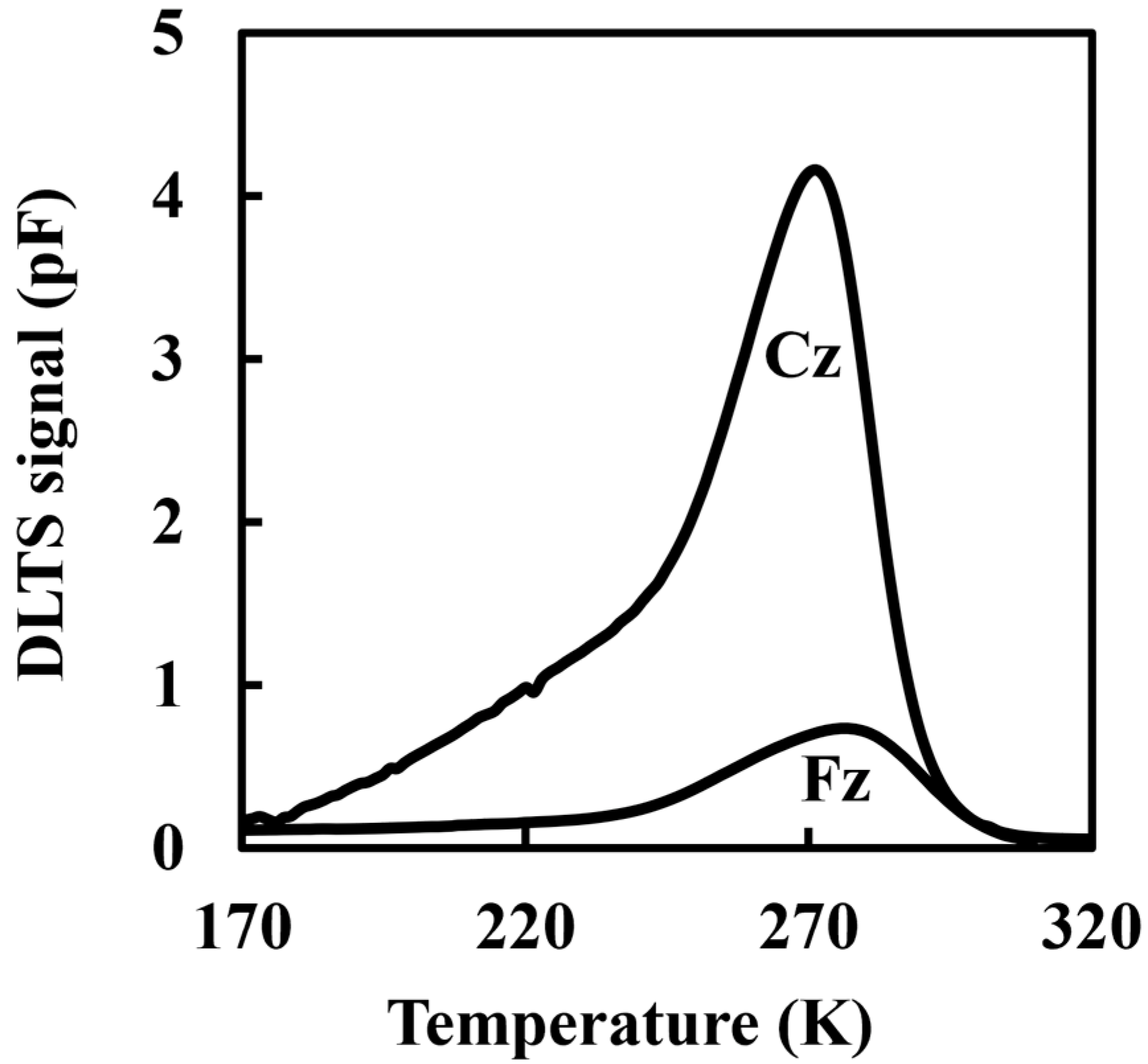
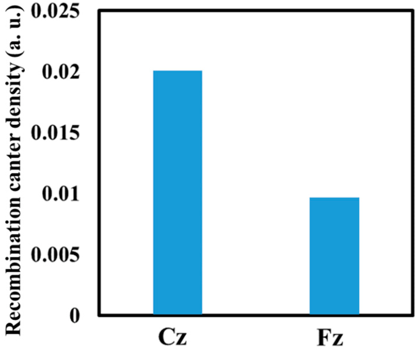
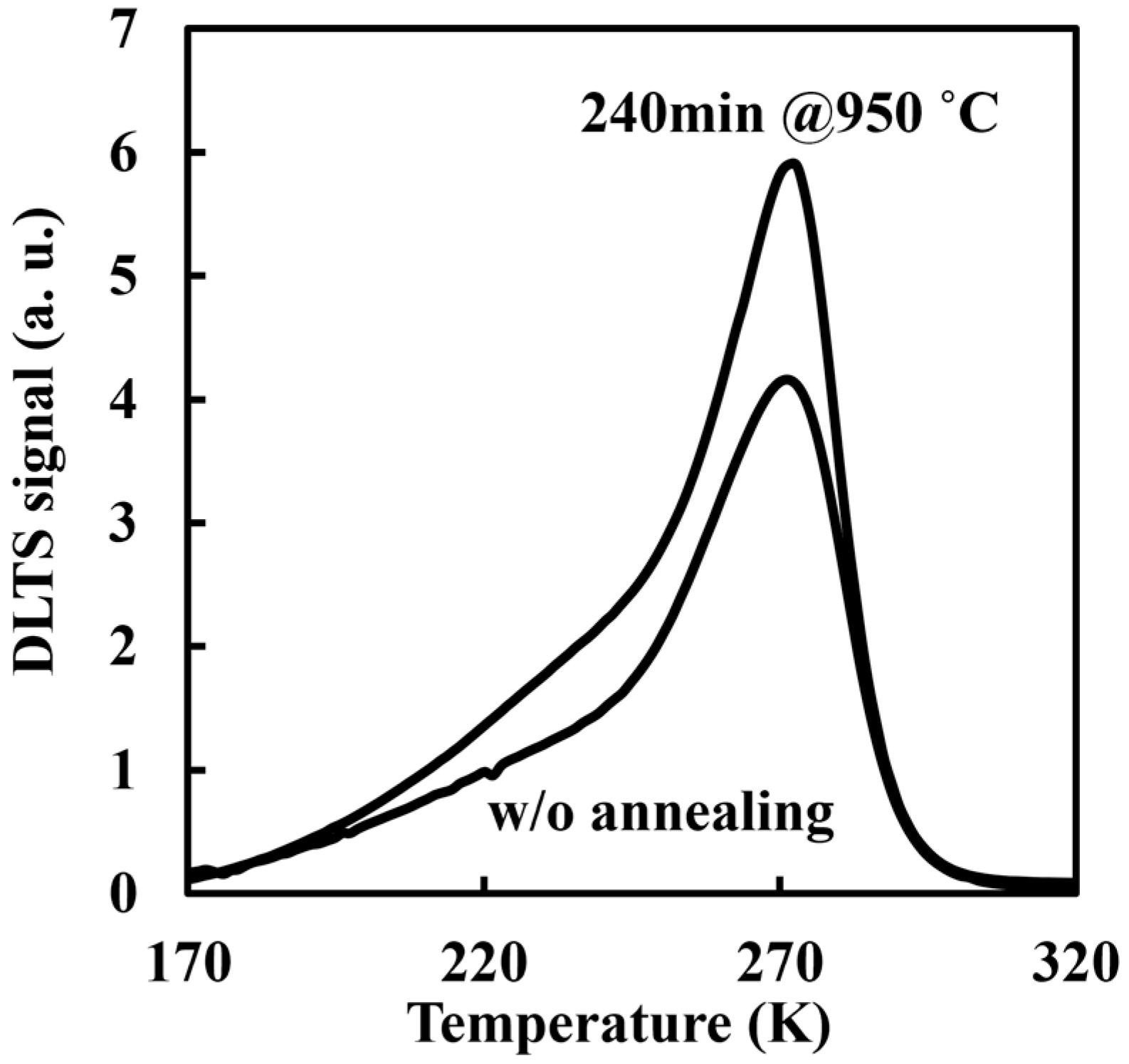
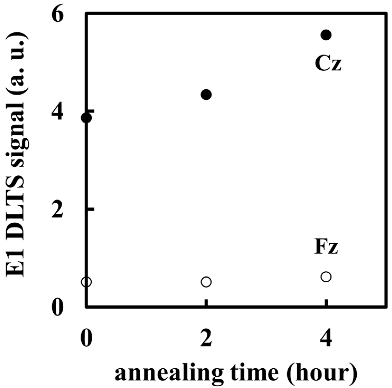
To study the effect of oxygen impurities in Si crystals on RPD-induced defects two types of phosphorous (P)-doped n-type Si (100) wafers with different oxygen concentrations were used as substrates. The first was a single silicon crystal grown using the CZ method. The oxygen concentration in the wafer was approximately 1018 atoms/cm3. The other was an FZ-grown silicon substrate containing 1015/cm3 oxygen atoms. The single-side mirror-polished wafers and double-side polished ones were used for minority carrier lifetime measurement and DLTS, respectively. Using these substrates, the (ITO)/SiO2/Si/SiO2/(ITO) and Al/(ITO)/SiO2/Si/Al structures were formed, as described below. A mixture of H2O, H2O2, and NH3 (5:1:1) was used to clean the wafers, and then the native oxide layer was removed from the HF solution. The unpolished side of the wafer was thermally doped, resulting in a relatively high P concentration (sheet resistivity of 60 Ω/sq.) to obtain ohmic contact at the backside of the DLTS sample.
Thin SiO2 layers were formed on these samples by dry oxidation under the O2 atmosphere at 950 °C. The thickness of the SiO2 layer was 10 nm, as determined using an ellipsometer. Then, the samples were annealed at 950 °C, with oxygen for 0, 120, and 240 min, the conditions under which precipitation would occur [30]. The RPD process deposited ITO films on the SiO2 layers. The Argon (Ar) plasma was generated in the plasma gun using an Ar supply; the flow rate of Ar gas was 20 sccm. Plasma was emitted into the growth chamber, and a magnetic field guided it to the ITO target. ITO evaporation formed approximately 90 nm thick ITO films on the substrate surfaces. Here, the source material was 5%wt Sn-doped ITO. Oxygen gas at a flow rate of 85 sccm was also supplied to the growth chamber, with the growth pressure maintained at 0.3 Pa. The substrate temperature was approximately 80 °C, which was not intentionally controlled or heated by plasma. To form the MOS structure, the deposited ITO film and back-side SiO2 layer were removed by the HCl and HF solution, respectively. Subsequently, both side surfaces were metalized with Al using the thermal evaporation system.
Using a quasi-steady-state photoconductance (QSSPC) measurement system (Sinton instruments WCT-120, Boulder, CO, USA), the minority carrier lifetimes of samples with and without deposited ITO were determined as a function of the injected carrier density [31]. DLTS measurements were performed [32,33,34,35,36]. MOS samples were placed in a vacuum chamber with a cryostat, and temperature scans were performed using a Boonton 72 B 1MHz bridge to obtain one second capacitance transients with 512 sampling points versus temperature T. T was varied from 120 K to 320 K. The transients were converted to DLTS signals by Fourier transform and DLTS spectra were obtained using the PhysTech DL8000 system. In the DLTS analysis, Bayesian optimization was used to obtain defect levels and capture cross sections by spectral deconvolution [28]. Assuming the time constant τ and DLTS signal S along with the theory of SRH process and DLTS, these values at a temperature T can be expressed as below.
τ T = 1 σ N v v t h e x p E c E t k B T
S t w ,   T = 2 A e x p t 0 τ T 1 e x p t w τ T 2 π t w 2 π 2 + 4 π 2 .
Here, in the Equation (1), Nv, vth, Ec, and kB are the density of states, thermal velocity, and Boltzmann constant, respectively. In Equation (2), tw is the period width of transient sampling, and A is a constant corresponding to the transient intensity. In this study, the pulse voltage for carrier injection and reverse voltage for carrier emission were 0 V and −1.5 V, respectively, and the period width tw was one second.
The objective function quantifies the difference in the spectral shape between the experimental and theoretical values drawn by the predicted property values. The predicted characteristic values Et and σ, corresponding to each defect, are optimized by self-consistently maximizing the objective function.

3. Results

The minority carrier lifetimes decreased because of the RPD process, regardless of the type of Si substrate. The recombination velocity was determined by the minority carrier lifetime at 1015 cm3 minority carrier density. This result shows that the SRH recombination process determines the minority carrier lifetime, and that the RPD induces recombination-active defects. The number of induced defects is shown in Figure 1. These were estimated from minority carrier lifetime at 1015 cm3 minority carrier density. These concentrations were determined as follows:
τ 1 N t v t h σ
where τ is carrier lifetime, Nt is defect density, vth is thermal velocity, and σ is capture cross-section. Although the RPD deposition conditions were the same, the number of RPD-induced recombination centers in Cz-Si was larger than that in the Fz wafer. This indicates that oxygen in the Si crystal may contribute to defect formation owing to the RPD process.
The DLTS spectra obtained for Cz-Si and Fz-Si are shown in Figure 2. New peaks around 270 K appeared in the DLTS spectra owing to the RPD process, and the signal intensity of Cz-Si was larger than that of Fz-Si, suggesting that the generated defect concentration was higher in Cz-Si than in Fz-Si. On the other hand, the peak positions are almost the same, regardless of the substrate type. Estimation of the physical properties of the induced defects was carried out using DLTS spectra. Bayesian optimization deconvoluted these spectra into three single peaks, indicating that three types of electron trap defects were generated in Fz-Si. Because the spectrum cannot be explained by using a single DLTS signal, spectra were deconvoluted by Bayesian optimization. These spectra were well described by the three peaks corresponding to the different types of electron trap defects generated in Si owing to the RPD process [28].
As well as the spectral deconvolution, the electrical defect properties used as search parameters were estimated in the Bayesian optimization. The obtained energy levels and capture cross-sections are summarized in Table 1. Because these defect properties are almost the same as those of the Cz-Si crystal, the same types of defects were induced by RPD, regardless of the crystal type. The E1 defect has a mid-gap energy level and approximately 10−15 cm2 capture cross-sections. This suggests that these defects might be recombination centers [27,28]. Because the types of defects are the same and their concentrations are different, it is suggested that the oxygen concentration in the Si crystal related to the number of induced defects.
The DLTS spectra change due to the 950 °C pre-annealing before the RPD process is shown in Figure 3. The signal was obtained from Cz-Si, with the peak intensity increasing owing to the annealing process. The defect concentration induced by the RPD process increased due to the annealing before the RPD process.
The relationship between the annealing time and E1 defect concentrations in the Cz and Fz Si crystals is shown in Figure 4. The signal intensity of Cz-Si increased as the annealing time increased. This indicates that oxygen precipitation might be related to the structure of RPD-induced defects. In contrast, in the case of Fz-Si, the increase of E1 defect signal intensity was very slight with increasing annealing time.

4. Conclusions

Suppression of the formation of crystal defects is essential for the realization of high-efficiency solar cells. The reactive plasma deposition (RPD) process introduces defects in the silicon crystal bulk and at the passivation layer/silicon crystal interface. This study suggests that oxygen impurities can affect the generation of reactive plasma deposition (RPD)-induced defects. Although the RPD deposition conditions were the same, the number of RPD-induced recombination centers in Cz-Si was larger than that in the Fz wafer. The increase in 950 °C pre-annealing increased the peak intensity corresponding to defect level E1, with 0.57 eV energy level in the Cz-Si MOS sample. In the case of Fz-Si, the increase in intensity was slight when pre-annealing time was increased to 4 h. This indicates that oxygen precipitation might be related to the structure of RPD-induced defects.

Author Contributions

Conceptualization, T.H. and Y.O.; methodology, T.H. and Y.O.; software, T.H. and Y.O.; validation, T.H. and Y.O.; formal analysis, T.H. and Y.O.; investigation, T.H. and Y.O.; resources, Y.O.; data curation, T.H., I.O., T.M.; writing—original draft preparation, T.H.; writing—review and editing, T.H. and Y.O.; visualization, T.H. and Y.O.; supervision, Y.O.; project administration, T.H. and Y.O.; funding acquisition, Y.O. All authors have read and agreed to the published version of the manuscript.

Funding

This work was supported by the Research Center for Smart Energy Technology under the Ministry of Education, Culture, Sports, Science and Technology, Japan.

Data Availability Statement

Not applicable.

Acknowledgments

This work was supported by the Research Center for Smart Energy Technology under the Ministry of Education, Culture, Sports, Science and Technology, Japan. And the authors thank Motoo Morimura and Mayuko Ohsugi at Toyota Technological Institute for their help in sample fabrication.

Conflicts of Interest

The authors declare no conflict of interest.

References

  1. Tyagi, A.; Biswas, J.; Ghosh, K.; Kottantharayil, A.; Lodha, S. Performance Analysis of Silicon Carrier Selective Contact Solar Cells With ALD MoOx as Hole Selective Layer. Silicon 2022, 14, 1663–1670. [Google Scholar] [CrossRef]
  2. Feldmann, F.; Simon, M.; Bivour, M.; Reichel, C.; Hermle, M.; Glunz, S.W. Carrier-Selective Contacts for Si Solar Cells. Appl. Phys. Lett. 2014, 104, 181105. [Google Scholar] [CrossRef]
  3. Dréon, J.; Jeangros, Q.; Cattin, J.; Haschke, J.; Antognini, L.; Ballif, C.; Boccard, M. 23.5%-Efficient Silicon Heterojunction Silicon Solar Cell Using Molybdenum Oxide as Hole-Selective Contact. Nano Energy 2020, 70, 104495. [Google Scholar] [CrossRef]
  4. Liu, Y.; Li, Y.; Wu, Y.; Yang, G.; Mazzarella, L.; Procel-Moya, P.; Tamboli, A.C.; Weber, K.; Boccard, M.; Isabella, O. High-Efficiency Silicon Heterojunction Solar Cells: Materials, Devices and Applications. Mater. Sci. Eng. R Rep. 2020, 142, 100579. [Google Scholar] [CrossRef]
  5. Yoshikawa, K.; Kawasaki, H.; Yoshida, W.; Irie, T.; Konishi, K.; Nakano, K.; Uto, T.; Adachi, D.; Kanematsu, M.; Uzu, H.; et al. Silicon Heterojunction Solar Cell with Interdigitated Back Contacts for a Photoconversion Efficiency over 26%. Nat. Energy 2017, 2, 17032. [Google Scholar] [CrossRef]
  6. Haschke, J.; Dupré, O.; Boccard, M.; Ballif, C. Silicon Heterojunction Solar Cells: Recent Technological Development and Practical Aspects—From Lab to Industry. Sol. Energy Mater. Sol. Cells 2018, 187, 140–153. [Google Scholar] [CrossRef]
  7. Green, M.A.; Dunlop, E.D.; Hohl-Ebinger, J.; Yoshita, M.; Kopidakis, N.; Ho-Baillie, A.W.Y. Solar Cell Efficiency Tables (Version 55). Prog. Photovolt. Res. Appl. 2020, 28, 3–15. [Google Scholar] [CrossRef]
  8. Bhattacharya, S.; John, S. Beyond 30% Conversion Efficiency in Silicon Solar Cells: A Numerical Demonstration. Sci. Rep. 2019, 9, 12482. [Google Scholar] [CrossRef]
  9. Meng, F.; Shi, J.; Shen, L.; Zhang, L.; Liu, J.; Liu, Y.; Yu, J.; Bao, J.; Liu, Z. Characterization of Transparent Conductive Oxide Films and Their Effect on Amorphous/Crystalline Silicon Heterojunction Solar Cells. Jpn. J. Appl. Phys. 2017, 56, 04CS09. [Google Scholar] [CrossRef]
  10. Li, L.; Du, G.; Lin, Y.; Zhou, X.; Gu, Z.; Lu, L.; Liu, W.; Huang, J.; Wang, J.; Yang, L. NiOx/MoOx Bilayer as an Efficient Hole-Selective Contact in Crystalline Silicon Solar Cells. Cell Rep. Phys. Sci. 2021, 2, 100684. [Google Scholar] [CrossRef]
  11. Nayak, M.; Mudgal, S.; Mandal, S.; Singh, S.; Komarala, V.K. Electrical Characterization and Defect States Analysis of Ag/ITO/MoOx/n-Si/LiFx/Al Carrier Selective Contact Solar Cells Processed at Room-Temperature. In AIP Conference Proceedings; AIP Publishing LLC: Melville, NY, USA, 2019; Volume 2147, p. 040014. [Google Scholar]
  12. Sen, M.T.S.K.A.; Bronsveld, P.; Weeber, A. Thermally Stable MoOx Hole Selective Contact with Al2O3 Interlayer for Industrial Size Silicon Solar Cells. Sol. Energy Mater. Sol. Cells 2021, 230, 111139. [Google Scholar] [CrossRef]
  13. Park, J.; Chang, H.S. Characteristics of Vanadium Oxide Grown by Atomic Layer Deposition for Hole Carrier Selective Contacts Si Solar Cells. Korean J. Mater. Res. 2020, 30, 660–665. [Google Scholar] [CrossRef]
  14. Munoz-Garcia, C.; Canteli, D.; Lauzurica, S.; Morales, M.; Molpeceres, C.; Ros, E.; Ortega, P.; López-González, J.M.; Voz, C. Influence of Wavelength and Pulse Duration on the Selective Laser Ablation of WOx, VOx and MoOx Thin Films. Surf. Interfaces 2022, 28, 101613. [Google Scholar] [CrossRef]
  15. Cruz, A.; Wang, E.-C.; Morales-Vilches, A.B.; Meza, D.; Neubert, S.; Szyszka, B.; Schlatmann, R.; Stannowski, B. Effect of Front TCO on the Performance of Rear-Junction Silicon Heterojunction Solar Cells: Insights from Simulations and Experiments. Sol. Energy Mater. Sol. Cells 2019, 195, 339–345. [Google Scholar] [CrossRef]
  16. Han, C.; Santbergen, R.; van Duffelen, M.; Procel, P.; Zhao, Y.; Yang, G.; Zhang, X.; Zeman, M.; Mazzarella, L.; Isabella, O. Towards Bifacial Silicon Heterojunction Solar Cells with Reduced TCO Use. Prog. Photovolt. Res. Appl. 2022, 30, 750–762. [Google Scholar] [CrossRef]
  17. Liu, H.; Gong, Y.; Diao, H.; Jia, X.; Zhao, L.; Wang, W.; Wang, W.; Zong, J. Comparative Study on IWO and ICO Transparent Conductive Oxide Films Prepared by Reactive Plasma Deposition for Copper Electroplated Silicon Heterojunction Solar Cell. J. Mater. Sci. Mater. Electron. 2022, 33, 5000–5008. [Google Scholar] [CrossRef]
  18. Han, C.; Zhao, Y.; Mazzarella, L.; Santbergen, R.; Montes, A.; Procel, P.; Yang, G.; Zhang, X.; Zeman, M.; Isabella, O. Room-Temperature Sputtered Tungsten-Doped Indium Oxide for Improved Current in Silicon Heterojunction Solar Cells. Sol. Energy Mater. Sol. Cells 2021, 227, 111082. [Google Scholar] [CrossRef]
  19. Kamioka, T.; Hayashi, Y.; Isogai, Y.; Nakamura, K.; Ohshita, Y. Analysis of Interface Workfunction and Process-Induced Damage of Reactive-Plasma-Deposited ITO/SiO2/Si Stack. AIP Adv. 2017, 7, 095212. [Google Scholar] [CrossRef]
  20. Linss, V.; Bivour, M.; Iwata, H.; Ortner, K. Comparison of Low Damage Sputter Deposition Techniques to Enable the Application of Very Thin A-Si Passivation Films; AIP Publishing LLC: Fes, Morocco, 2019; p. 040009. [Google Scholar]
  21. Tachibana, T.; Takai, D.; Kojima, T.; Kamioka, T.; Ogura, A.; Ohshita, Y. Minority Carrier Recombination Properties of Crystalline Defect on Silicon Surface Induced by Plasma Enhanced Chemical Vapor Deposition. ECS J. Solid State Sci. Technol. 2016, 5, Q253–Q256. [Google Scholar] [CrossRef]
  22. Kamioka, T.; Isogai, Y.; Hayashi, Y.; Ohshita, Y.; Ogura, A. Effects of Damages Induced by Indium-Tin-Oxide Reactive Plasma Deposition on Minority Carrier Lifetime in Silicon Crystal. AIP Adv. 2019, 9, 105219. [Google Scholar] [CrossRef]
  23. Kuwano, K.; Ashok, S. Investigation of Sputtered Indium-Tin Oxide/Silicon Interfaces: Ion Damage, Hydrogen Passivation and Low-Temperature Anneal. Appl. Surf. Sci. 1997, 117–118, 629–633. [Google Scholar] [CrossRef]
  24. Kitami, H.; Miyashita, M.; Sakemi, T.; Aoki, Y.; Kato, T. Quantitative Analysis of Ionization Rates of Depositing Particles in Reactive Plasma Deposition Using Mass-Energy Analyzer and Langmuir Probe. Jpn. J. Appl. Phys. 2015, 54, 01AB05. [Google Scholar] [CrossRef]
  25. Iwata, K.; Sakemi, T.; Yamada, A.; Fons, P.; Awai, K.; Yamamoto, T.; Shirakata, S.; Matsubara, K.; Tampo, H.; Sakurai, K.; et al. Improvement of ZnO TCO Film Growth for Photovoltaic Devices by Reactive Plasma Deposition (RPD). Thin Solid Film. 2005, 480–481, 199–203. [Google Scholar] [CrossRef]
  26. Onishi, K.; Hara, Y.; Nishihara, T.; Kanai, H.; Kamioka, T.; Ohshita, Y.; Ogura, A. Evaluation of Plasma Induced Defects on Silicon Substrate by Solar Cell Fabrication Process. Jpn. J. Appl. Phys. 2020, 59, 071003. [Google Scholar] [CrossRef]
  27. Hara, T.; Ohshita, Y. Analysis of Recombination Centers near an Interface of a Metal–SiO 2 –Si Structure by Double Carrier Pulse Deep-Level Transient Spectroscopy. AIP Adv. 2022, 12, 095316. [Google Scholar] [CrossRef]
  28. Hara, T.; Lee, H.; Kawanishi, M.; Ohshita, Y. DLTS with Bayesian Inference for Analyzing RPD Induced Defects in Bulk near SiO2/Si Interface. ECS J. Solid State Sci. Technol. 2022, 11, 035002. [Google Scholar] [CrossRef]
  29. Hara, T.; Tanaka, T.; Nakagawa, K.; Isogai, Y.; Kamioka, T.; Ohshita, Y. Light Induced Recombination Center at SiO2/Si Interface by the Reactive Plasma Deposition. Electron. Mater. Lett. 2021, 17, 399–405. [Google Scholar] [CrossRef]
  30. Borghesi, A.; Pivac, B.; Sassella, A.; Stella, A. Oxygen Precipitation in Silicon. J. Appl. Phys. 1995, 77, 4169–4244. [Google Scholar] [CrossRef]
  31. Sinton, R.A.; Cuevas, A. Contactless Determination of Current–Voltage Characteristics and Minority-carrier Lifetimes in Semiconductors from Quasi-steady-state Photoconductance Data. Appl. Phys. Lett. 1996, 69, 2510–2512. [Google Scholar] [CrossRef]
  32. Lang, D.V. Deep-Level Transient Spectroscopy: A New Method to Characterize Traps in Semiconductors. J. Appl. Phys. 1974, 45, 3023–3032. [Google Scholar] [CrossRef]
  33. Das, A.; Singh, V.A.; Lang, D.V. Deep-Level Transient Spectroscopy (DLTS) Analysis of Defect Levels in Semiconductor Alloys. Semicond. Sci. Technol. 1988, 3, 1177. [Google Scholar] [CrossRef]
  34. Lang, D.V.; Logan, R.A. A Study of Deep Levels in GaAs by Capacitance Spectroscopy. J. Electron. Mater. 1975, 4, 1053–1066. [Google Scholar] [CrossRef]
  35. Weiss, S.; Kassing, R. Deep Level Transient Fourier Spectroscopy (DLTFS)—A Technique for the Analysis of Deep Level Properties. Solid-State Electron. 1988, 31, 1733–1742. [Google Scholar] [CrossRef]
  36. Kósa, A.; Stuchlíková, L.; Dawidowski, W.; Jakus, J.; Sciana, B.; Radziewicz, D.; Pucicki, D.; Harmatha, L.; Kovac, J.; Tlaczala, M. DLTFS Investigation of InGaAsN/GaAs Tandem Solar Cell. J. Electr. Eng. 2014, 65, 271. [Google Scholar] [CrossRef]
Figure 1. The recombination center densities in Cz-Si and Fz-Si estimated with minority carrier lifetime.
Crystals 13 00310 g001
Figure 2. DLTS spectra obtained from Cz-Si and Fz-Si MOS sample processed with RPD.
Crystals 13 00310 g002
Figure 3. The increase of DLTS signal intensity by the 950 °C pre-annealing.
Crystals 13 00310 g003
Figure 4. The relationship between annealing time and E1 defect concentrations.
Crystals 13 00310 g004
Table 1. Estimated electrical property of RPD-induced defects, where Ec − Et is the defect level from conduction band edge Ec, and σ is the capture cross-section for majority carriers.
CzFz
Ec − Et (eV)σ (cm2)Ec − Et (eV)σ (cm2)
E10.575.5 × 10−150.567.2 × 10−15
E20.517.2 × 10−150.56.3 × 10−15
E30.472.5 × 10−160.455.1 × 10−15
Disclaimer/Publisher’s Note: The statements, opinions and data contained in all publications are solely those of the individual author(s) and contributor(s) and not of MDPI and/or the editor(s). MDPI and/or the editor(s) disclaim responsibility for any injury to people or property resulting from any ideas, methods, instructions or products referred to in the content.

