Article

Terahertz Electromagnetically Induced Transparency with Electric-Field-Coupled Inductor-Capacitor Resonators on LCP Substrate

1
QILU Aerospace Information Research Institute (AIR), Chinese Academy of Sciences (CAS), Jinan 250132, China
2
Shandong Technology Center of Nanodevices and Integration and School of Microelectronics, Shandong University, Jinan 250100, China
3
Institute of Radioelectronics and Multimedia Technology, Warsaw University of Technology, 00-665 Warsaw, Poland
4
State Key Laboratory of Transducer Technology, Aerospace Information Research Institute (AIR), Chinese Academy of Sciences (CAS), Beijing 100190, China
*
Authors to whom correspondence should be addressed.
Crystals 2023, 13(2), 283; https://doi.org/10.3390/cryst13020283
Submission received: 17 January 2023 / Revised: 4 February 2023 / Accepted: 6 February 2023 / Published: 7 February 2023
(This article belongs to the Special Issue Terahertz Metamaterials and Active Modulation)

Abstract

:
Electromagnetically induced transparency (EIT) metamaterials (MTMs) based on the bright-dark mode theory have gained great interest in slow light, sensing, and energy storage in recent years. Typically, various split ring resonators with magnetic response have been proposed as dark resonators in EIT MTMs. Here, we have employed a cut-wire (CW) and two electric-field-coupled inductor-capacitor (ELC) resonators with a pure electrical response on a liquid crystal polymer (LCP) substrate with a low loss tangent to fulfill the EIT effect in the terahertz (THz) region. The former works as the bright mode, and the latter functions as the dark mode. The EIT phenomenon results from the destructive interference between these two modes, which can be verified by numerical simulation and near field distribution. In addition, a Lorentz oscillator model was studied to quantitatively analyze the relationship between the coupling strength and the coupling distance. As a demonstration, an EIT MTM device with 5000 units was fabricated and characterized, which showed a transmission window with a peak value of 0.75 at 0.414 THz. This work may inspire new multifunctional EIT MTMs, especially the flexible applications at THz frequencies.

1. Introduction

Electromagnetically induced transparency (EIT) arises from the destructive interference phenomenon between the two quantum transition paths in a three-level atomic system, leading to an abnormal transmission peak within a broad absorption spectrum and a large group delay accompanied by a significant attenuation of the group velocity [1,2]. With the advantages of the strongly dispersive nature and the enhancement of nonlinear susceptibility in the transmission window, EIT has found many important applications, such as slow light [3], enhancing nonlinear interactions [4], and memories [5]. However, the realization of the typical atomic EIT effect requires some harsh working conditions including ultra-low temperature and high intensity pumping, which prevents its on-chip integration. To overcome the listed drawbacks, various classical systems have been demonstrated to mimic the EIT effect, such as electric circuits [6], plasmonic structures [7], microcavity [8], photonic crystal waveguides [9] and metamaterials (MTMs) [10,11,12,13,14,15,16,17,18,19,20,21].
Metamaterials are periodic functional structures consisting of subwavelength metallic or dielectric “meta-atoms”, which exhibit abnormal abilities to freely tailor electromagnetic waves at infrared and below [22]. Metamaterials possess the ability to enhance the interaction between electromagnetic waves and media, and thus have found many promising applications in sensing [23,24], communications [25] and nonlinear devices [26]. Recently, the EIT analogues in MTMs have gained great interest due to its slow light effects and profile miniaturization, enabling many advances in sensing [10], filtering [11], energy storage [12], switching [13], etc. In general, the unit cell of EIT MTMs is composed of two coupled resonators with dissimilar absorption responses at similar frequencies, namely bright and dark modes, respectively. These resonators in two modes usually employ metal materials, which limits the achievable quality factor (Q-factor) of EIT phenomenon to less than 10 because of the inherent ohmic loss [14]. Therefore, some high-refractive-index dielectric MTMs with smaller intrinsic loss have been proposed to achieve high Q-factor [15,16]. Almost all the reported bright mode resonators, whether metallic or dielectric, are cut-wires (CW) [15,16,17] and square rings [18], which can be directly excited by incident waves to generate a broad absorption band. The dark mode resonators excited by the near field coupling of the bright mode resonators have a high Q-factor response and produce interference phenomenon, subduing the absorption of the bright resonator, and thus inducing a narrow transmission peak. As typical magnetic response elements, split ring resonators (SRRs) have become the most common dark mode resonators in metallic and dielectric EIT MTMs, and further support the realization of multi-frequency response [12], active regulation [13,17,19,20], and polarization insensitivity [18,21]. For dielectric EIT MTMs, silicon rings and silicon disks supporting magnetic dipole modes have also been designed as dark modes [15,16]. In contrast, high symmetric units with purely electrical response and negative permittivity, i.e., electric-field-coupled inductor-capacitor (ELC) resonators [27], have never been reported as dark mode resonators up to now.
To improve the transmission peak of EIT MTMs, the substrate typically needs low loss tangent, low permittivity, and small thickness, which may become a big constraint at terahertz (THz) frequencies with small wavelength. The THz band, lying between microwave and infrared frequencies, has enormous potential in advanced communication and sensing applications because of its peculiar properties, such as spectral fingerprint, non-ionization, and rich spectrum resources [28]. At THz frequencies, the most widely used substrate is high-resistivity silicon, whose permittivity is as large as 11.9 [22]. In addition, its substrate thickness is typically larger than 200 μm, and its cost is high with respect to the polymers. Alternatively, the common polyethylene terephthalates (PET) [29] and polyimides (PI) [30] exhibit large loss tangent at THz frequencies. Liquid crystal polymers (LCP) substrate is a perfect candidate for THz MTMs because of its flexibility, low dielectric constant (~3), low loss tangent, and small thickness down to 25 μm [31]. Current reports on LCP-based MTMs focuses on microwave [32] and millimeter wave [33] frequencies, while the research in terahertz band needs to be further developed.
In this work, a novel LCP-based MTMs with purely electrical response resonators is designed and demonstrated for the first time, achieving the well-known EIT effect at THz frequencies. The proposed EIT MTM unit is composed of a CW and two ELC resonators, which function as the bright and dark resonators, respectively. The internal working mechanism between these two resonators are demonstrated by the simulated field distributions and surface current densities. In simulation, the EIT MTM unit has a transmission peak of 0.86 at 0.41 THz. The maximum value of the group delay is 11.67 at 0.41 THz and the minimum value is −63.4 ps at 0.38 THz, respectively. The coupling distances have been discussed to clarify the impact of unit cell parameters on the performance of the EIT phenomenon. To illustrate the flexible performance accurately and visually, a bending model was built by using the wrap sheet method for the change of transmission peak under different curvature radius. Furthermore, theoretical research based on the effective Lorentz oscillation model was applied to quantitatively reveal the coupling process between the CW and the ELC resonators. The spectrum curves calculated from the double oscillator model perfectly matched the simulation data. To verify this design, a device with 5000 EIT MTM units was manufactured and tested, showing a peak value of 0.75 and a Q-factor of 9 at 0.414 THz. This work paves a new way for EIT MTM structures and their flexible applications in the THz range.

2. Design and Simulation

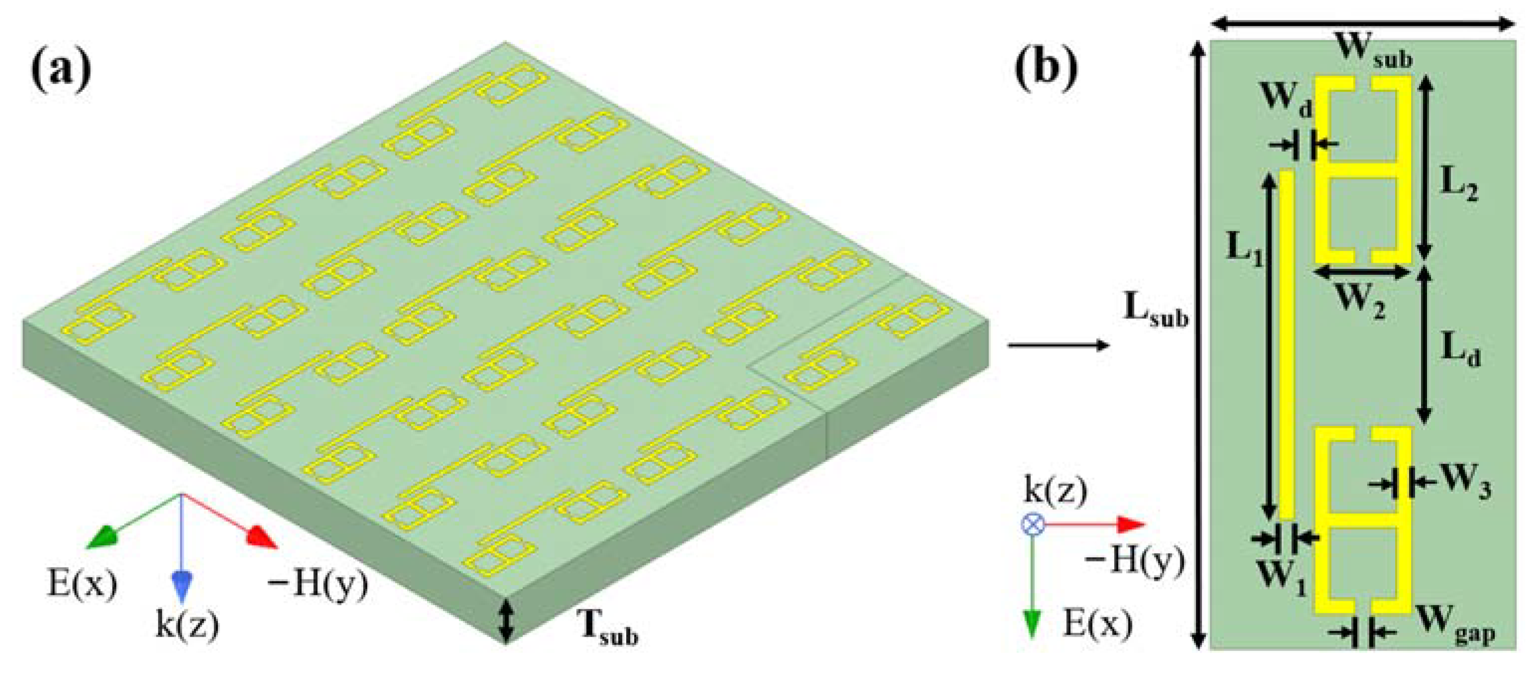
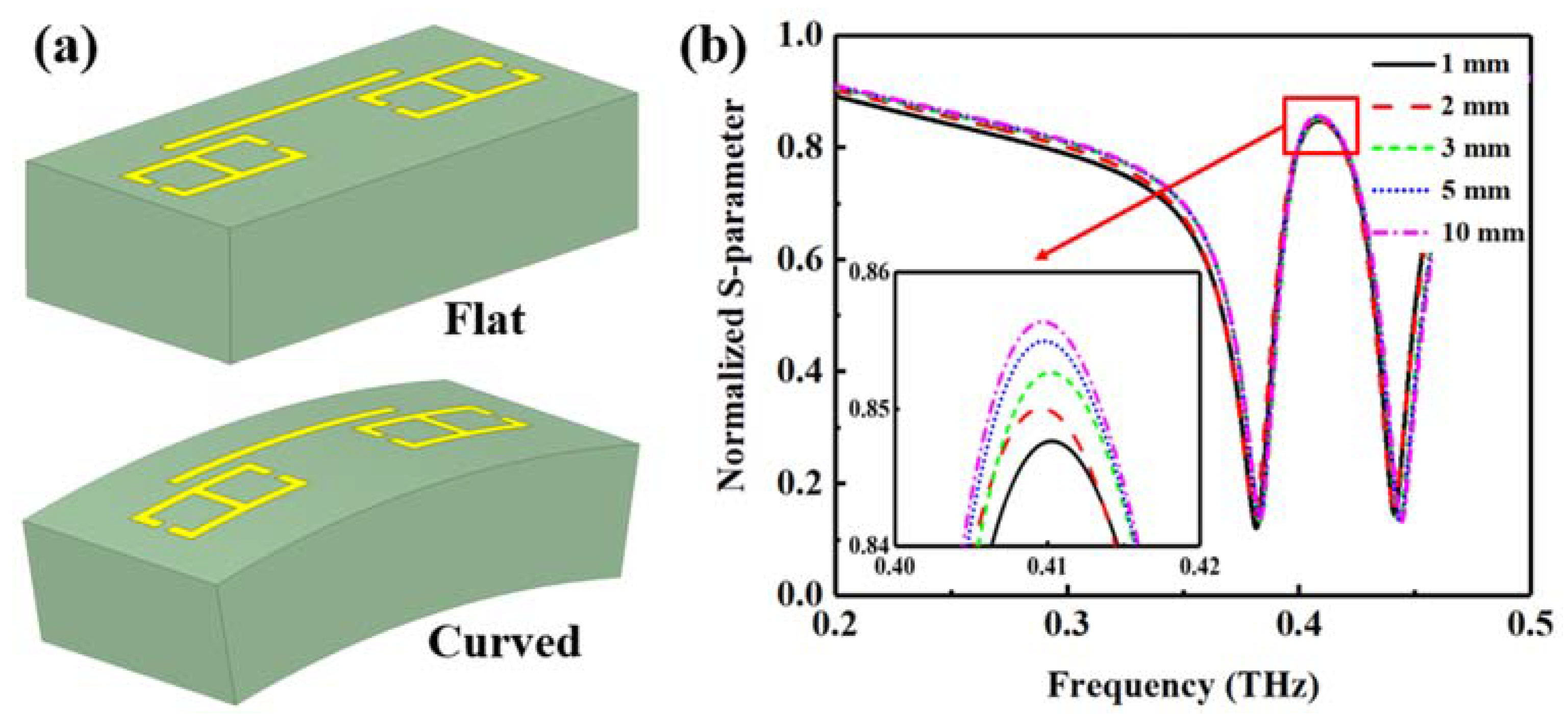
2.1. Structural Design

Figure 1a illustrates the schematic configuration of the proposed EIT MTM device and the polarization of the incident plane terahertz waves. To suppress the dielectric loss and develop flexible applications at THz band, the EIT MTM was placed on a 100 μm thick liquid crystal polymers (LCP) substrate with a relative permittivity of 3.27 and a loss tangent of 0.002. These MTM patterns were set as gold with a thickness of 300 nm. As shown in Figure 1b, the EIT MTM unit cell was composed of a CW and two conventional ELC resonators located on the same side of the CW. The detail structural parameters are listed in the caption of Figure 1. The horizontal and vertical lattice constants were Wsub = 200 μm and Lsub = 400 μm, respectively. The length and width of the CW were L1 = 230 μm and W1 = 10 μm, respectively. The length, width, wire width and gap width of the ELC resonator were L2 = 124 μm, W2 = 64 μm, W3 = 10 μm, Wgap = 10 μm, respectively. The vertical coupling distance between the two ELC resonators was Ld = 106 μm. The horizontal coupling distance between the CW and the ELC resonators was Wd = 13 μm.
The ELC resonator was composed of two or four SRRs, which is a kind of metamaterial with both central symmetry and axial symmetry [34]. Compared with the SRR resonators, the ELC resonators eliminate the magneto-optical coupling effects, while mainly exhibit purely an electrical resonant response to the electric field. The real part curve of the effective permittivity extracted from the ELC resonator in this work is depicted in Figure 2a and shows a significant negative dielectric response. There is a sharp switch from 4.268 to −5.771 at 0.42 THz in the real part curve. Note that the ELC resonator can be directly excited by the incident waves. The polarization direction of the incident waves is shown in the inset in Figure 2a. For the CW, the real part curve of the effective permittivity is shown in Figure 2b. The real part curve has a peak value of 21.27 at 0.42 THz, which corresponds to the absorption enhancement of the CW. When the two ELC resonators were symmetrically placed on the same side of the CW without overlapping, the intrinsic peak value of the CW dropped to 1.68 and disappeared, as illustrated in Figure 2c. At the same time, the real part curve of the EIT MTM had two peaks with relatively small value of 8.09 and 16.56 at 0.38 and 0.45 THz, respectively. The effective permittivity in the pass band was about 1.3. Typically, the working mechanisms of the ELC structure can be regarded as a simplified RLC circuit model [22]. As shown in Figure 2d, R is the resistance, C represents the capacitance of the split, L represents the cumulative inductance of the half metallic loop, V represents the magnitudes of induced voltage. The resonant frequency of the proposed ELC structure can be described as the following equation:
f = 2 2 π L C   .
Ansys High Frequency Structure Simulator (HFSS) software was used to design and optimize their performance. In the 3-D model of the proposed EIT MTM units, the periodic boundary conditions were added in both x-directions and y-directions, and z-direction was used as the wave propagating direction. The obtained signal amplitude of the electromagnetic waves transmitted through the device was normalized to the incident waves and named as normalized transmission.

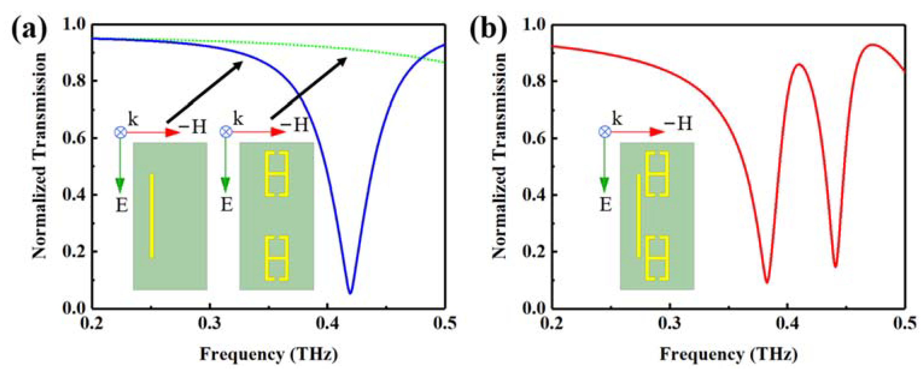
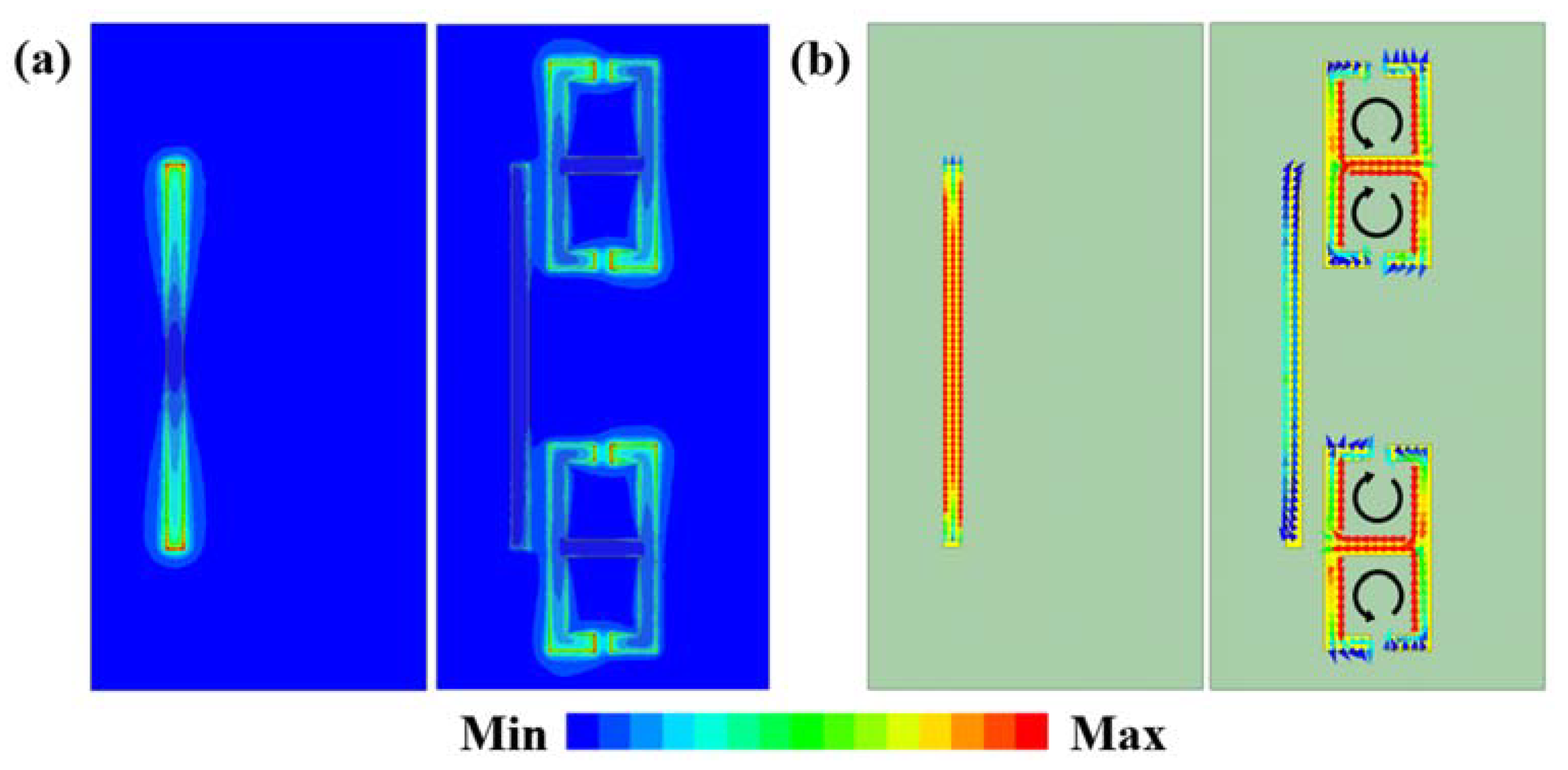
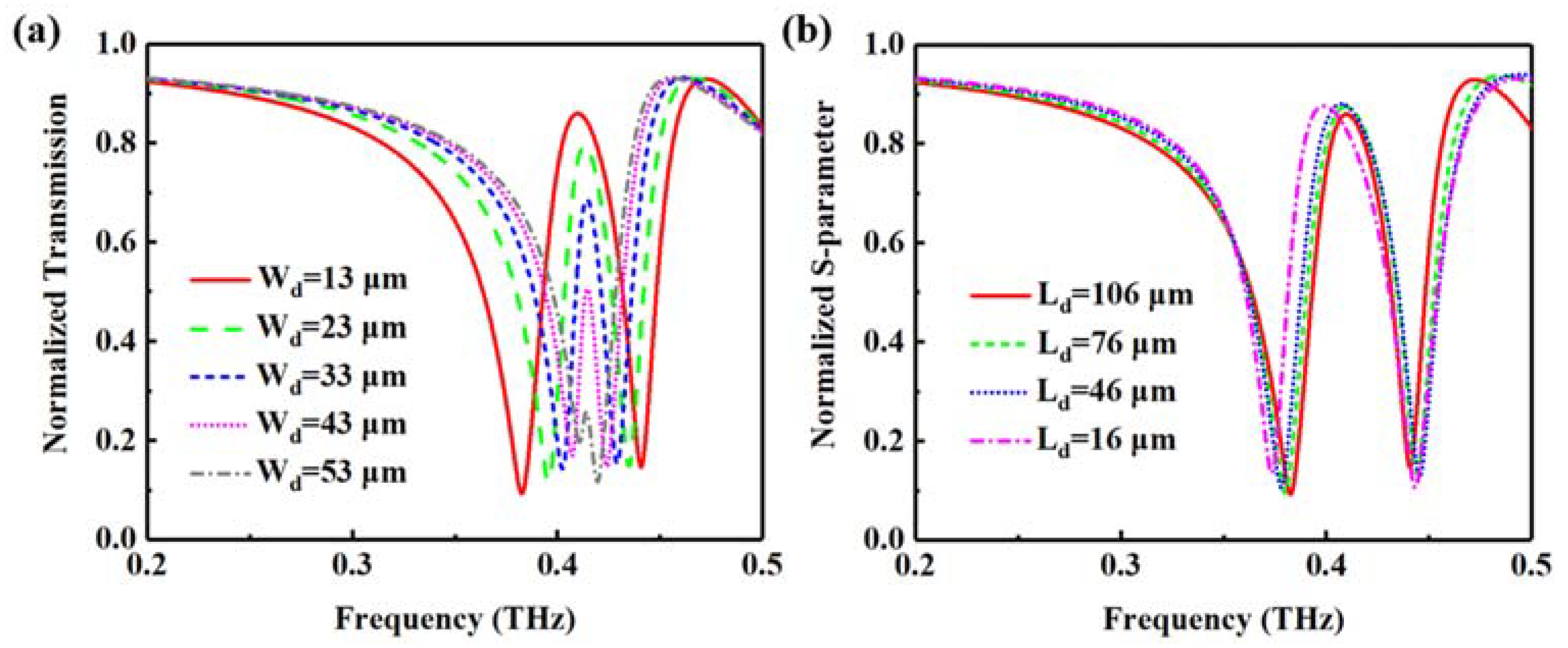
2.2. Numerical Simulation

The simulated transmission curves of the CW, ELC resonator and EIT MTM under y-direction polarized incident terahertz waves are illustrated in Figure 3. As depicted in Figure 3a, the CW is directly excited by incident waves to generate a broad absorption band at 0.42 THz, which exhibits a typical local surface plasmon (LSP) resonance mode. The normalized transmission at the resonant frequency was only 0.05. The ELC resonator with similar resonant frequency showed a gradual transmission curve without any significant absorption responses in the transmission spectra as it cannot be excited by the y-direction polarized incident waves. However, by combining the CW and two ELC resonators in a unit cell with a close coupling distance, a narrow transmission peak appeared at the frequency which was similar to the resonant frequency of the CW, as illustrated in Figure 3b. In the normalized transmission curve, the narrow transmission peak was 0.86 at 0.41 THz, and the two valleys were 0.09 and 0.15 at 0.38 and 0.44 THz, respectively. The transmission curves were in good agreement with the real part curves of the effective permittivity. The Q-factor of the peak can be extracted by the following equation:
Q = f 0 W f   .
where f 0 is the ratio of the center frequency and W f is the full width at half maximum (FWHM). The W f is 0.042 THz, so the corresponding Q-factor of the transmission peak is 13. In this structure, the CW acts as bright resonator for its direct coupling with the y-direction polarized incident waves while the ELC structures serve as dark resonators for their near-field coupling with the bright resonator.
Apart from the transmission peak, the slow light effect is another essential feature of the EIT phenomenon [18]. The slow light effect is the phenomenon of transmission delay when the terahertz waves transmit through the EIT MTMs, which is caused by the severe dispersion of the transmission phase. As illustrated in Figure 4a, a sharp phase dispersion appears around the transmission peak of the proposed EIT MTMs. The group delay defined as − φ ω / ω is depicted in Figure 4b, where φ is the transmission phase, ω represents the angular resonant frequency, and φ ω represents the phase shift of the incident waves [35]. The maximum group delay at the EIT frequency reached 11.67 ps, which corresponds to the propagation distance of 3.5 mm that light can travel freely in vacuum. The minimum group delay is −63.4 ps at 0.38 THz. The delay-bandwidth product (DBP) obtained from the maximum group delay and W f was 0.49, leading to the potential of slow light devices.
To explore the near field coupling mechanism within the EIT MTM, the electric field distributions and surface current densities of the CW and EIT MTMs at resonant frequency are illustrated in Figure 5. As depicted in Figure 5a, the electric fields of the CW concentrate on both ends as an electric dipole mode under the direct excitation of the incident waves. For the EIT MTM, the electric fields mainly concentrated around the split gaps of the ELC resonators, which is the characteristic of a typical EIT effect. The electric fields of the CW became subdued, due to the strong near field coupling between the CW and the ELC resonators. The radiation waves generated by the accumulated charges in the split gaps were polarized orthogonally to the incident waves, resulting in the cross-polarized transmission and the narrow transmission peak [35]. The surface current densities of the CW and EIT MTM are simulated in Figure 5b, which can further indicate the transformation mechanisms. Under the excitation of an external stimuli, the surface current intensity of the CW with respect to the polarization direction of the electric field of incident waves is greater than that in the proposed EIT MTM. For the EIT MTM, it can be observed that the induced circulating currents of the two SRR parts of each ELC resonator have opposite directions, which evidences the fundamental LC resonance of the ELC resonators. The surface currents of the SRRs near the center of the unit cell were in the clockwise direction, while those of the other half SRRs were counterclockwise, so the main resonance on the ELC resonators was electrical resonance. In general, the resonance coupling between the CW and the ELC resonators completely suppressed the radiation loss of the bright mode, resulting in the EIT phenomenon at the resonant frequency.
To clarify the impact of unit cell parameters on the performance of the EIT effect, the normalized transmission spectra with different horizontal and vertical coupling distance (i.e., Wd and Ld) are depicted in Figure 6. Other structural parameters mainly affect the resonant frequencies of the CW and the ELC resonator, so they are not discussed in this paper. As shown in Figure 6a, as the horizontal coupling distance Wd varied from 13 to 53 μm, the normalized transmission gradually decreased from 0.86 to 0.25, and the transmission peak red-shifted from 0.41 THz to 0.414 THz. The increase of horizontal coupling distance corresponded to the decrease of coupling strength between the CW and the ELC resonators, which led to the increasing similarity of transmission curves of the EIT MTM and the CW. The normalized transmission curves with different vertical coupling distance Ld are illustrated in Figure 6b. As the vertical coupling distance varied from 106 to 46 μm, the value of the transmission peak gradually changed from 0.86 to 0.88 at 0.41 THz with a blue shift of 2 GHz. This almost negligible impact shows that the vertical coupling distance had little effect on the performance of the EIT effect when it was greater than 46 μm. When the vertical coupling distance was further reduced to 16 μm, the transmission peak was 0.88 at 0.398 THz, showing a significant blue shift of 12 GHz due to the strong electric field coupling between the two ELC resonators.
In general, the bending substrate has a remarkable impact on the resonant frequency and the peak value of the transmission peak [32,36]. To estimate the influence of the bending LCP substrate on the transmission curve, a curved model that can be bent with arbitrary curvature radius was built in HFSS using the wrap sheet method, as shown in Figure 7a. Figure 7b illustrates the normalized transmission spectra of the proposed EIT MTM with different curvature radii. The curvature radius is inversely proportional to the degree of curvature. When the curvature radius was 10 mm, the transmission peak value was 0.856 at 0.41 THz. As the curvature radius decreased to 1 mm, the peak gradually decreased to 0.847 and maintained the same frequency, which is in good agreement with the trend in the literature [36]. At the same time, the normalized transmission loss increased by about 0.023 on average in the pass band.

3. Theory and Experiment

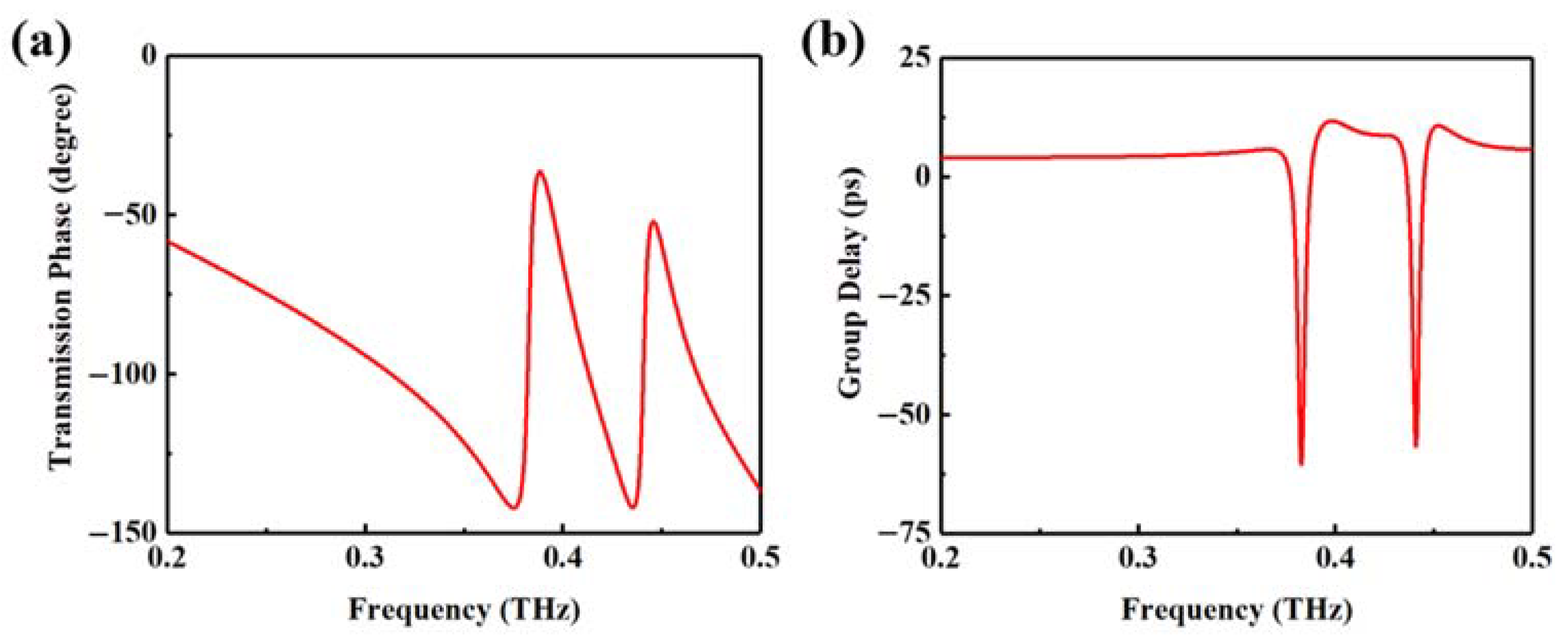
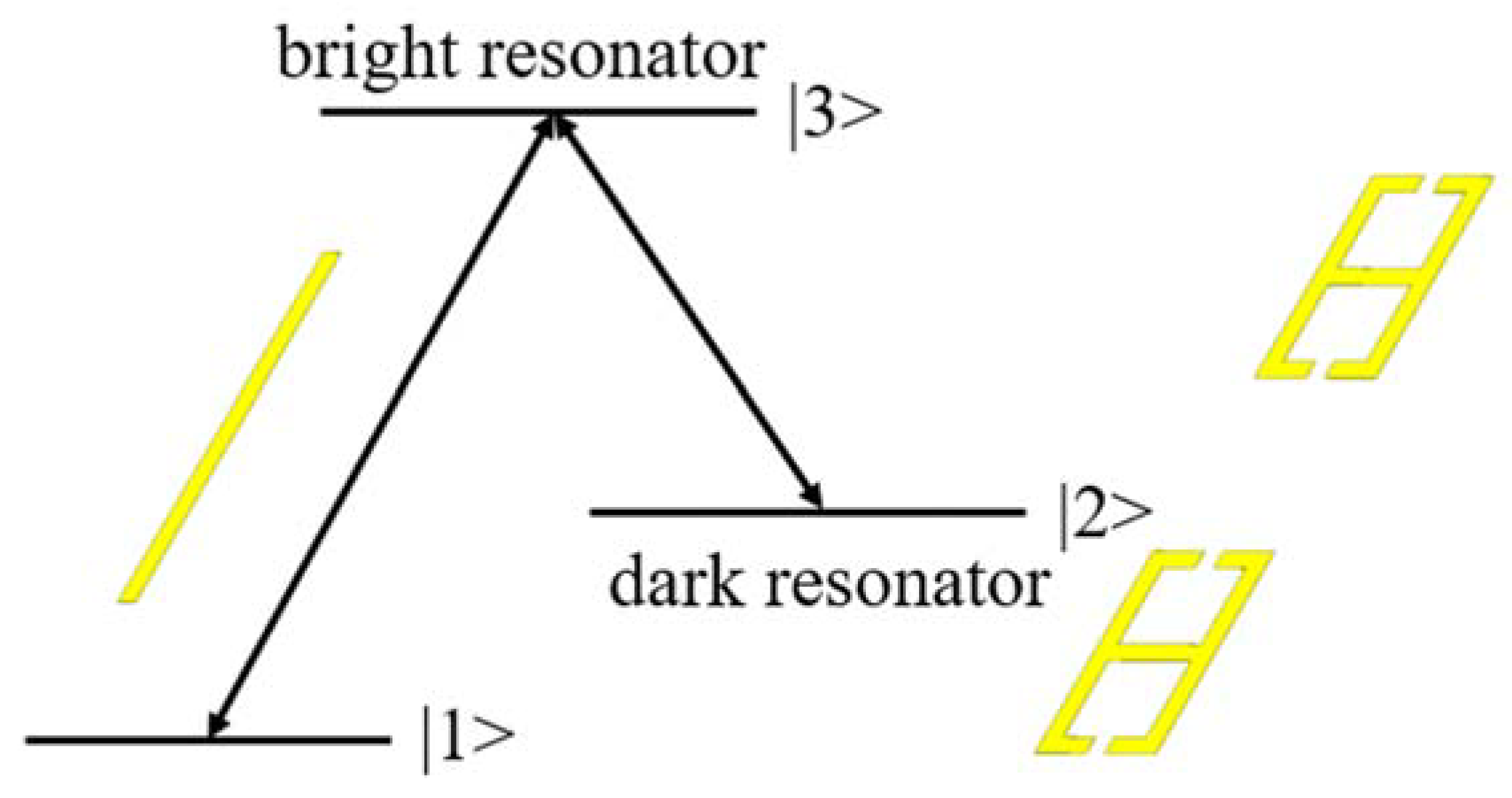
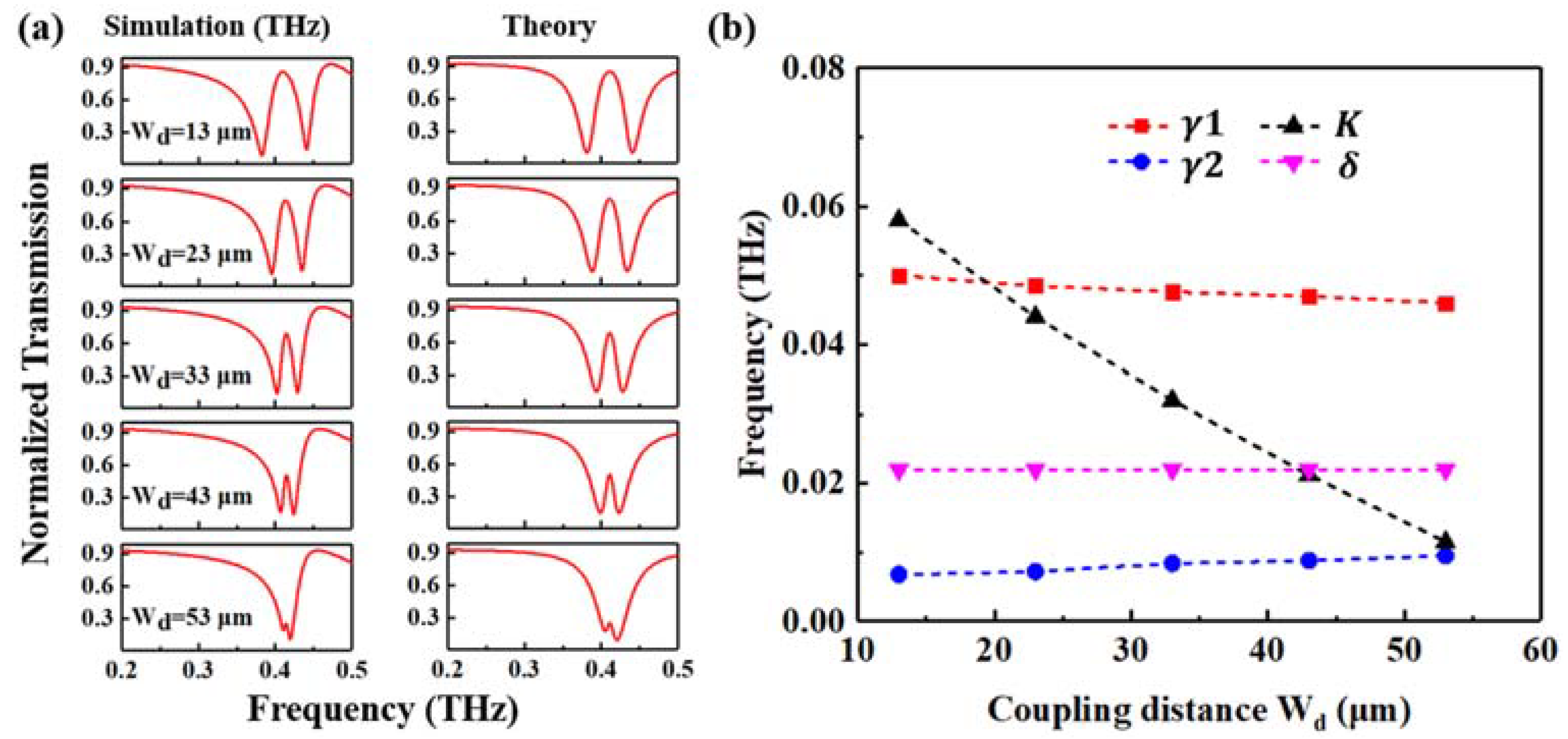
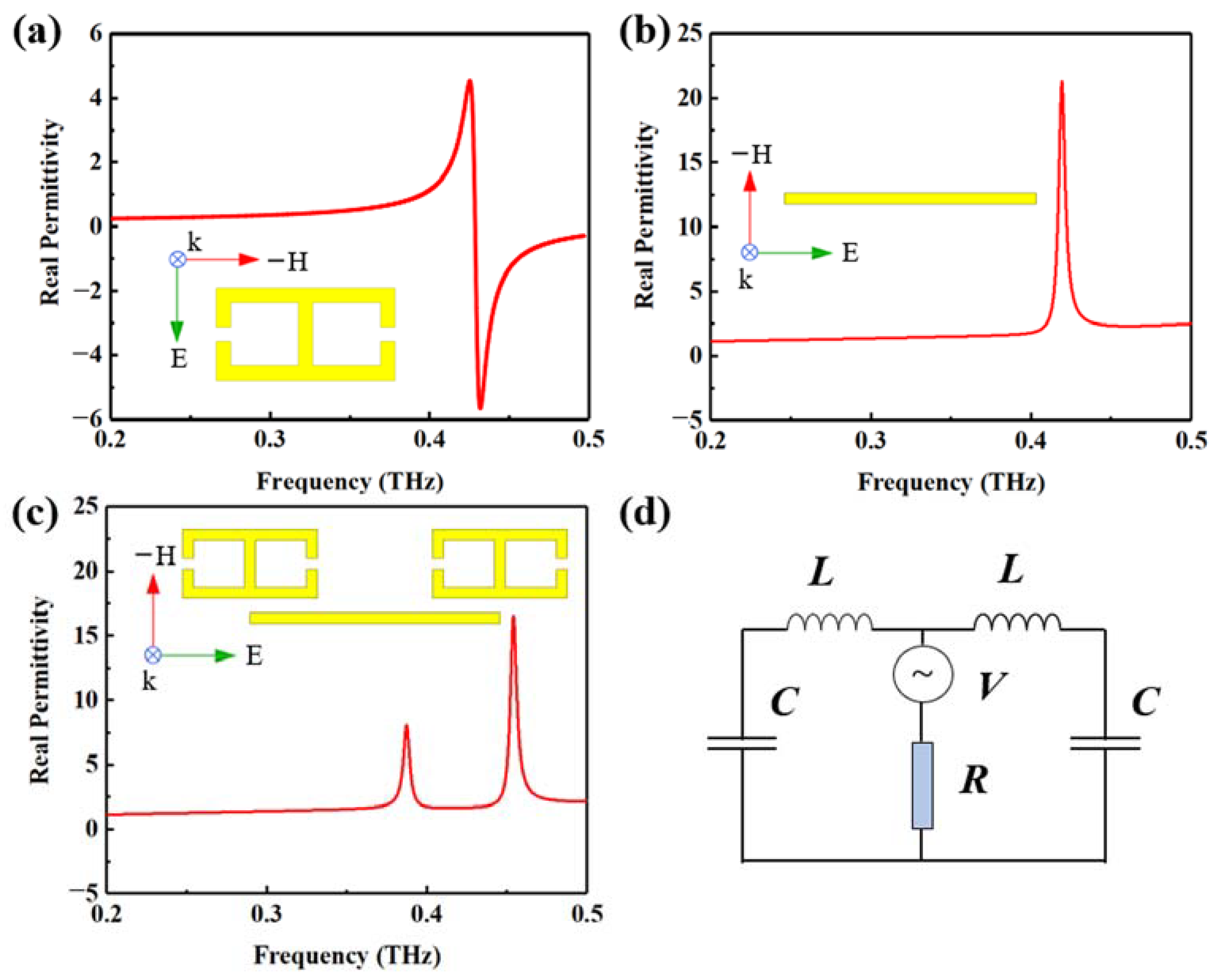
3.1. Theoretical Analysis

Typically, the physical principle of the EIT phenomenon can be described as a three-level atomic system [37]. In this design, the atomic system composed of the ground state energy |1>, the high energy level |2> and the excitation state energy |3> was mapped to the coupling process of the CW and ELC resonators, as shown in Figure 8. The process from |1> to |2> represents that the CW is excited by the incident waves, and the process from |2> to |3> represents that the near field coupling between the CW and the ELC resonators. Meanwhile, the ELC resonators can be excited by the x-direction polarized incident waves, corresponding to the process from |1> to |3>. These two different excitation paths in the proposed EIT MTM system led to a destructive interference phenomenon.
To further theoretically analyze the physical origin of the EIT phenomenon, a classical Lorentz oscillator model was used to quantitatively analysis the coupling effect between the CW and the ELC resonator [19]. The coupled oscillators satisfy the following equations:
x 1 ¨ + γ 1 x 1 ˙ + ω 0 2 x 1 + κ x 2 = g E   ,
x 2 ¨ + γ 2 x 2 ˙ + ω 0 + δ 2 x 2 + κ x 1 = 0   .
where x 1 , x 2 , γ 1 and γ 2 are the resonant amplitudes and the damping rates of the CW and ELC resonator, respectively. ω 0 and ω 0 + δ represent the angular resonant frequencies of the CW and ELC resonator, respectively. δ and κ represent the mismatch of the resonant frequency and the coupling coefficient between the CW and the ELC resonator, respectively. G represents geometric parameter indicating the coupling strength between the CW and the incident electric field. By simultaneously solving the Equations (3) and (4) based on the approximation ω ‹‹ ω 0 , the susceptibility χ and the transmission T of the proposed EIT MTM can be expressed as:
χ = χ r + i χ i   ω ω 0 + δ + i γ 2 2 ω ω 0 + i γ 1 2 ω ω 0 + δ + i γ 2 2 κ 2 4   ,
T = 1 g χ i   .
The simulation curves and theoretically fitting transmission spectra of the EIT MTM with various horizontal coupling distances Wd are shown in Figure 9a, in which two sets of spectrum curves are in good agreement. The fitting parameters γ 1 , γ 2 , δ and κ , as a function of the horizontal coupling distance, are shown in Figure 9b, which theoretically validates the near field coupling mechanism. When Wd = 13 μm, the fitting parameters were γ 1 = 0.05 THz, γ 2 = 0.0068 THz, δ = 0.022 THz, and κ = 0.058 THz2, respectively. As the horizontal coupling distance increased from 13 to 53 μm, it was observed that γ 1 gradually decreased from 0.05 to 0.046 THz, whereas γ 2 increased markedly from 0.0068 to 0.0095 THz. The unchanged δ means that the transmission peak frequency always maintains 0.41 THz. The significant decline of κ indicates the attenuation of the destructive interference between the CW and the ELC structures.

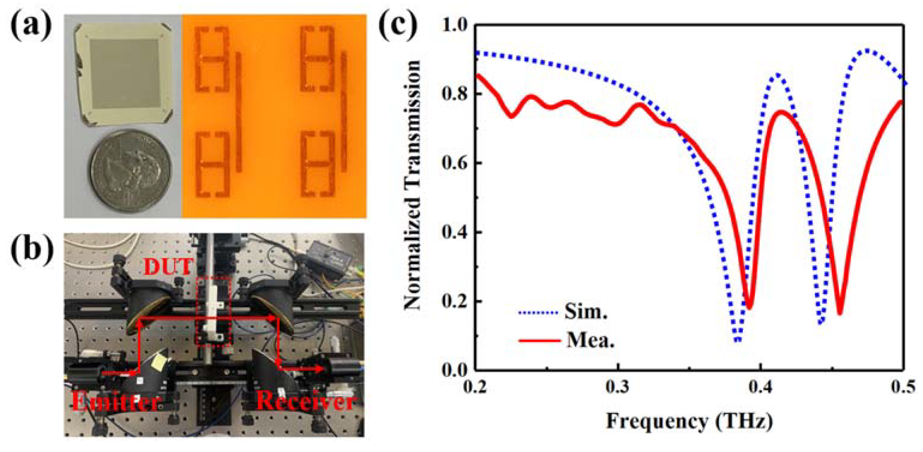
3.2. Experimental Verification

To verify the above-mentioned structure, an EIT MTM device was manufactured on a 100-μm thick LCP substrate, containing a total of 5000 EIT MTM units, as illustrated in Figure 10a. The size of the whole device was similar to that of China’s one-yuan coin. The LCP substrate was ultrasonically cleaned in isopropanol, absolute ethanol, and de-ionized water for five minutes before processing. The metal pattern was composed of 30 nm titanium (Ti) and 170 nm gold (Au) from bottom to top by standard ultraviolet lithography, electron-beam evaporation, and lift-off technology. Toptica THz frequency-domain spectroscopy (FDS) TeraScan 1550 was applied to characterize the fabricated EIT MTM device [22]. The experimental setup is shown in Figure 10b, where the device under test (DUT) is located in the center of the optical path. The radius of the collimated beam was nearly 1 mm. The test resolution was set to 30 MHz. The test was carried out at room temperature and 10% humidity.
The measured transmission curve of the fabricated EIT MTM device is depicted in Figure 10c. A significant transmission peak appeared at 0.414 THz with a peak value of 0.75 and a Q-factor of 9. The 3-dB bandwidth was 46 GHz, corresponding to 11% of the operating frequency. The two valleys at 0.39 and 0.45 THz were 0.194 and 0.179, respectively. Compared to the simulated results, the blue shift of the transmission peak and valleys mainly came from the manufacturing tolerance. In addition, the thin metal thickness of the fabricated device reduced the interaction between the EIT MTM and the incident terahertz waves, and thus led to a transmission attenuation of the peak and the pass band.
Table 1 shows the comparison of the experimental results between this work and the reported EIT MTMs in terms of the type of dark mode resonator, the value of normalized transmission peak, group delay, 3-dB bandwidth, flexibility, and substrate types. The thickness of the LCP substrate in this work (100 μm) was far less than that of F4B (2 mm), sapphire (495 μm) and glass (500 μm) substrates in the references. Apart from the ELC resonator and the flexible LCP substrate, the proposed EIT MTM device has many advantages, such as large transmission peak, large group delay and similar 3-dB bandwidth, which is especially suitable for slow light and sensing applications.

4. Conclusions

To summarize, we designed and fabricated an EIT MTM with ELC resonators on a flexible LCP substrate for the first time, achieving a significant EIT effect at THz frequencies. The ELC resonators with purely electrical response can be excited by the CW through near field coupling, and thus generating a destructive interference phenomenon. The proposed device provides a new insight into the EIT MTM design and its flexible applications in the THz regime and may be combined with active components to offer some fascinating possibilities, such as the frequency switching of EIT phenomenon.

Author Contributions

Conceptualization, H.L. and Y.Z. (Yifei Zhang); methodology, H.L. and Y.Z. (Yifei Zhang); software, H.L., X.X. and Y.Z. (Yifei Zhang); validation, H.L., Z.L. and K.L.; formal analysis, H.L.; investigation, H.L., Y.Z. (Yongping Zhou) and J.L.; resources, X.Z. and Y.Z. (Yifei Zhang); data curation, H.L., R.Z. and P.M.; writing—original draft preparation, H.L.; writing—review and editing, H.L., Y.Y. and Y.Z. (Yifei Zhang); visualization, H.L.; supervision, H.L. and Y.Z. (Yifei Zhang); project administration, H.L.; funding acquisition, X.Z. and Y.Z (Yifei Zhang). All authors have read and agreed to the published version of the manuscript.

Funding

This work was supported by the National Key Research and Development Program of China under Grant 2022YFA1405200, the National Natural Science Foundation of China under Grant 61701283, the China Postdoctoral Science Foundation funded project under Grant 2018T110689 and 2017M622201, and the Postdoctoral Innovation Program of Shandong Province under Grant 20171006.

Data Availability Statement

Not applicable.

Conflicts of Interest

The authors declare no conflict of interest.

References

  1. Harris, S.E. Electromagnetically induced transparency. Phys. Today 1997, 50, 36–42. [Google Scholar] [CrossRef]
  2. Fleischhauer, M.; Imamoglu, A.; Marangos, J.P. Electromagnetically induced transparency: Optics in coherent media. Rev. Mod. Phys. 2005, 77, 633–673. [Google Scholar] [CrossRef]
  3. Lukin, M.; Imamoglu, A. Controlling photons using electromagnetically induced transparency. Nature 2001, 413, 273–276. [Google Scholar] [CrossRef] [PubMed]
  4. Zhang, Y.P.; Brown, A.W.; Xiao, M. Opening four-wave mixing and six-wave mixing channels via dual electromagnetically induced transparency windows. Phys. Rev. Lett. 2007, 99, 123603. [Google Scholar] [CrossRef]
  5. Lvovsky, A.I.; Sanders, B.C.; Tittel, W. Optical quantum memory. Nat. Photonics 2009, 3, 706–714. [Google Scholar] [CrossRef]
  6. Harden, j.; Joshi, A.; Serna, J.D. Demonstration of double EIT using coupled harmonic oscillators and RLC circuits. Eur. J. Phys. 2011, 32, 541. [Google Scholar] [CrossRef]
  7. Dyer, G.C.; Aizin, G.R.; Allen, S.J.; Grine, A.D.; Bethke, D.; Reno, J.L.; Shaner, E.A. Induced transparency by coupling of Tamm and defect states in tunable terahertz plasmonic crystals. Nat. Photonics 2013, 7, 925–930. [Google Scholar] [CrossRef]
  8. Liu, Y.C.; Li, B.B.; Xiao, Y.F. Electromagnetically induced transparency in optical microcavities. Nanophotonics 2017, 6, 789–811. [Google Scholar] [CrossRef]
  9. Yang, X.D.; Yu, M.B.; Kwong, D.L.; Wong, C.W. All-optical analog to electromagnetically induced transparency in multiple coupled photonic crystal cavities. Phys. Rev. Lett. 2019, 102, 173902. [Google Scholar] [CrossRef]
  10. Askari, M.; Bahadoran, M. A refractive-index-based microwave sensor based on classical electromagnetically induced transparency in metamaterials. Optik 2022, 253, 168589. [Google Scholar] [CrossRef]
  11. Nagarajan, A.; Erve, K.V.; Gerini, G. Ultra-narrowband polarization insensitive transmission filter using a coupled dielectric-metal metasurface. Opt. Express 2020, 28, 773–787. [Google Scholar] [CrossRef] [PubMed]
  12. Zheng, S.Q.; Ma, M.S.; Lv, Y.; Fu, T.; Peng, L.; Zhao, Q.X. Dual-band electromagnetically induced transparent metamaterial with slow light effect and energy storage. J. Phys. D Appl. Phys. 2022, 55, 255103. [Google Scholar] [CrossRef]
  13. Hu, Y.Z.; Tong, M.Y.; Hu, S.Y.; He, W.B.; Cheng, X.A.; Jiang, T. Multidimensional engineered metasurface for ultrafast terahertz switching at frequency-agile channels. Nanophotonics 2022, 11, 1367–1378. [Google Scholar] [CrossRef]
  14. He, F.Y.; Han, B.X.; Li, X.J.; Lang, T.T.; Jing, X.F.; Hong, Z. Analogue of electromagnetically induced transparency with high-Q factor in metal-dielectric metamaterials based on bright-bright mode coupling. Opt. Express 2019, 27, 37590–37600. [Google Scholar] [CrossRef] [PubMed]
  15. Yang, Y.M.; Kravchenko, I.I.; Briggs, D.P.; Valentine, J. All-dielectric metasurface analogue of electromagnetically induced transparency. Nat. Commun. 2014, 5, 5753. [Google Scholar] [CrossRef]
  16. Hua, M.; Sun, Y.B.; Li, M.P.; Liu, Z.Z.; Chen, Y.; Shi, Y.P.; Ning, Y.F.; Zhang, Y.F.; Yang, F.H.; Wang, X.D. Electromagnetically induced transparency analog in terahertz hybrid metal–dielectric metamaterials. AIP Adv. 2021, 11, 065309. [Google Scholar] [CrossRef]
  17. Zhang, J.; Li, Z.F.; Shao, L.D.; Xiao, F.J.; Zhu, W.R. Active modulation of electromagnetically induced transparency analog in graphene-based microwave metamaterial. Carbon 2021, 183, 850–857. [Google Scholar] [CrossRef]
  18. Han, L.; Tan, Q.L.; Gan, Y.; Zhang, W.D.; Xiong, J.J. Polarization-insensitive classical electromagnetically induced transparency metamaterial with large group delay by Dirac semimetal. Results Phys. 2020, 19, 103377. [Google Scholar] [CrossRef]
  19. Gu, J.; Singh, R.; Liu, X.; Zhang, X.; Ma, Y.; Zhang, S.; Maier, S.A.; Tian, Z.; Azad, A.K.; Chen, H.-T.; et al. Active control of electromagnetically induced transparency analogue in terahertz metamaterials. Nat. Commun. 2012, 3, 1151. [Google Scholar] [CrossRef]
  20. Kim, T.T.; Kim, H.D.; Zhao, R.K.; Oh, S.S.; Ha, T.; Chung, D.; Lee, Y.H.; Min, B.; Zhang, S. Electrically tunable slow light using graphene metamaterials. ACS Photonics 2018, 5, 1800–1807. [Google Scholar] [CrossRef]
  21. Zhang, J.; Mu, N.; Liu, L.H.; Xie, J.H.; Feng, H.; Yao, J.Q.; Chen, T.N.; Zhu, W.R. Highly sensitive detection of malignant glioma cells using metamaterial-inspired THz biosensor based on electromagnetically induced transparency. Biosens. Bioelectron. 2021, 185, 113241. [Google Scholar] [CrossRef] [PubMed]
  22. Ling, H.T.; Qian, P.F.; Zhang, B.Q.; Feng, M.M.; Wang, Y.M.; Zhang, X.J.; Wang, Q.P.; Zhang, Y.F.; Song, A.M. Active terahertz metamaterials electrically modulated by InGaZnO Schottky diodes. Opt. Mater. Express 2021, 11, 2966–2974. [Google Scholar] [CrossRef]
  23. Karthikeyan, M.; Jayabala, P.; Ramachandran, S.; Dhanabalan, S.S.; Sivanesan, T.; Ponnusamy, M. Tunable optimal dual band metamaterial absorber for high sensitivity THz refractive index sensing. Nanomaterials 2022, 12, 2693. [Google Scholar] [CrossRef] [PubMed]
  24. Li, Z.R.; Cheng, Y.Z.; Luo, H.; Chen, F.; Li, X.C. Dual-band tunable terahertz perfect absorber based on all-dielectric InSb resonator structure for sensing application. J. Alloys Compd. 2022, 925, 166617. [Google Scholar] [CrossRef]
  25. Zhang, L.; Chen, M.Z.; Tang, W.K.; Dai, J.Y.; Miao, L.; Zhou, X.Y.; Jin, S.; Cheng, Q.; Cui, T.J. A wireless communication scheme based on space- and frequency-division multiplexing using digital metasurfaces. Nat. Electron. 2021, 4, 218–227. [Google Scholar] [CrossRef]
  26. Bae, M.H.; Oh, J.H. Nonlinear elastic metamaterial for tunable bandgap at quasi-static frequency. Mech. Syst. Signal Process. 2022, 170, 108832. [Google Scholar] [CrossRef]
  27. Schurig, D.; Mock, J.J.; Smith, D.R. Electric-field-coupled resonators for negative permittivity metamaterials. Appl. Phys. Lett. 2006, 88, 041109. [Google Scholar] [CrossRef]
  28. Xu, W.D.; Xie, L.J.; Ying, Y.B. Mechanisms and applications of terahertz metamaterial sensing: A review. Nanoscale 2017, 9, 13864–13878. [Google Scholar] [CrossRef]
  29. Pitchappa, P.; Kumar, A.; Prakash, S.; Jani, H.; Medwal, R.; Mishra, M.; Rawat, R.S.; Venkatesan, T.; Wang, N.; Singh, R. Volatile ultrafast switching at multilevel nonvolatile states of phase change material for active flexible terahertz metadevices. Adv. Funct. Mater. 2021, 31, 2100200. [Google Scholar] [CrossRef]
  30. Qu, Z.; Xu, Y.Q.; Zhang, B.Z.; Duan, J.P.; Tian, Y. Terahertz dual-band polarization insensitive electromagnetically induced transparency-like metamaterials. Plasmonics 2020, 15, 301–308. [Google Scholar] [CrossRef]
  31. Zhou, Z.; Li, W.; Qian, J.; Liu, W.; Wang, Y.; Zhang, X.; Guo, Q.; Yashchyshyn, Y.; Wang, Q.; Shi, Y.; et al. Flexible liquid crystal polymer technologies from microwave to terahertz frequencies. Molecules 2022, 27, 1336. [Google Scholar] [CrossRef]
  32. Li, W.; Lan, Y.; Wang, H.P.; Xu, Y.H. Microwave polarizer based on complementary split ring resonators frequency-selective surface for conformal application. IEEE Access 2021, 9, 111383–111389. [Google Scholar] [CrossRef]
  33. Nguyen, V.N.; Yönak, S.H.; Smit, D.R. Multilayer-band artificial dielectric on liquid crystal polymer. IEEE Antenn. Wirel. Propag. Lett. 2010, 9, 974–977. [Google Scholar] [CrossRef]
  34. Padilla, W.J.; Aronsson, M.T.; Highstrete, C.; Lee, M.; Taylor, A.J.; Averitt, R.D. Electrically resonant terahertz metamaterials: Theoretical and experimental investigations. Phys. Rev. B 2007, 75, 041102. [Google Scholar] [CrossRef]
  35. Yang, T.; Liu, X.M.; Zhou, J. Terahertz polarization conversion in an electromagnetically induced transparency (EIT)-like metamaterial. Ann. Phys. 2021, 533, 2000528. [Google Scholar] [CrossRef]
  36. Lee, D.; Lee, D.; Yun, H.S.; Kim, D.S. Angstrom-scale active width control of nano slits for variable plasmonic cavity. Nanomaterials 2021, 11, 2463. [Google Scholar] [CrossRef]
  37. Dong, H.Q.; Gao, C.J.; Zeng, L.; Zhang, D.; Zhang, H.F. Investigating on the electromagnetically induced absorption metamaterial in the terahertz region realized by the multilayer structure. Physica B 2022, 639, 413936. [Google Scholar] [CrossRef]
Figure 1. Schematic of the proposed EIT MTM device and the coordinate systems. (a) Periodic array. (b) Top view of one unit cell. (Tsub = 100 μm, Wsub = 200 μm, Lsub = 400 μm, L1 = 230 μm, W1 = 10 μm, L2 = 124 μm, W2 = 64 μm, W3 = 10 μm, Wgap = 10 μm, Ld = 106 μm, Wd = 13 μm). The coordinate systems show the corresponding polarization direction of the incident waves.
Crystals 13 00283 g001
Figure 2. (ac) Real part curves of the permittivity of the ELC resonator, CW, and EIT MTM unit cell. The insets and coordinate systems show the corresponding unit cells and the polarization direction of the incident waves. (d) Equivalent circuit of the ELC resonator.
Crystals 13 00283 g002
Figure 3. (a) Normalized transmission curves of the CW (blue solid line) and ELC resonators (green dotted line). (b) Normalized transmission curve of the proposed EIT MTM. The insets and coordinate systems show the corresponding unit cells and the polarization direction of the incident waves.
Crystals 13 00283 g003
Figure 4. (a) Transmission phase of the proposed EIT MTM unit. (b) Group delay of the proposed EIT MTM extracted from the transmission curve.
Crystals 13 00283 g004
Figure 5. (a) Electric field distributions of the CW and EIT MTM at resonant frequency. (b) Surface current densities of the CW and EIT MTM at resonant frequency. The black arrow shows the direction of the induced current.
Crystals 13 00283 g005
Figure 6. Normalized transmission spectra of the proposed EIT MTM with (a) different horizontal coupling distance Wd from 13 to 53 μm and (b) different vertical coupling distance Ld from 16 to 106 μm.
Crystals 13 00283 g006
Figure 7. (a) Schematic of the flat and curved EIT MTM unit cells. (b) Simulated transmission spectra of the proposed EIT MTM unit cell with different curvature radius. The inset shows an enlarged view around the transmission peak.
Crystals 13 00283 g007
Figure 8. Three-level atomic system model of the proposed EIT MTMs.
Crystals 13 00283 g008
Figure 9. (a) Simulation curves and theoretical fitting transmission curves of the proposed EIT MTM with the coupling distance Wd from 13 to 53 μm. (b) The fitting parameters used in the theoretical transmission spectra. The unit of κ is THz2.
Crystals 13 00283 g009
Figure 10. (a) Photograph and the enlarged view of the fabricated EIT MTM device. (b) Photograph of the test setup. (c) Measured (red solid line) and simulated (blue dotted line) transmission curves of the fabricated EIT MTM device.
Crystals 13 00283 g010
Table 1. Comparison with the experimental results of EIT MTMs already reported.
Ref.Dark Mode ResonatorTransmission
(a.u.)
Group Delay (ps)3-dB Bandwidth
(%)
Flexibility
(Y or N)
Substrate Types
[17]SRR0.62>10008%NF4B
[19]SRR0.855.7413.5%NSapphire
[20]SRR0.53.1Unknown 1YPI
[21]SRR0.47Unknown 211%NGlass
This workELC0.7511.6711%YLCP
1 The transmission peak is too low to calculate the 3-dB bandwidth. 2 The group delay is not discussed in the article.
Disclaimer/Publisher’s Note: The statements, opinions and data contained in all publications are solely those of the individual author(s) and contributor(s) and not of MDPI and/or the editor(s). MDPI and/or the editor(s) disclaim responsibility for any injury to people or property resulting from any ideas, methods, instructions or products referred to in the content.

