Abstract
Solar cells can be designed for indoor applications to provide a feasible solution for harnessing photon energy from indoor lighting. In this paper, we analyze the suitability of a selenium-based solar cell for gathering photon energy emitted by indoor light-emitting diodes (LEDs). The absorption band of selenium (Se) is found to be aligned with the LED spectrum, making it a promising contender for efficient indoor applications. In order to simulate the Se-based photovoltaic (PV) device, we started by calibrating the simulation model against a fabricated Se cell that was tested under AM1.5G. After the verification of the physical models and the technological key factors of the different layers incorporated in cell design, a systematic approach was performed to assess the operation of the Se solar cell under an LED light environment. We show an optimized power conversion efficiency (PCE) of 26.93% for the Se-based cell under LED illumination (311 μW/cm2). This is achieved by providing an effective design that incorporates a double-ETL structure, which can significantly improve the band alignment between the different layers of the cell device. The simulation results presented in this work serve to judge the potential of Se solar cells as indoor PVs and offer an approach for providing indoor use specifically designed for internet-of-things (IoT) devices.
1. Introduction
Photovoltaic (PV) technologies have emerged as a central renewable energy resource, portraying a fundamental role in addressing accelerating energy demands and environmental apprehensions. The capability of solar cells to collect sun energy and convert it into electricity has acquired immense interest worldwide because of their immaculate and sustainable nature [1,2]. By harnessing solar energy, these devices contribute to reducing reliance on fossil fuels. Thin-film solar cells (TFSCs) have undergone overwhelming advances due to their potential for lightweight structures, high absorption coefficient, and ease of incorporation into several applications [3,4,5]. TFSCs notably offer significant benefits over traditional crystalline silicon-based solar cells, such as lower processing costs and enhanced versatility in material selection [6,7].
While solar cells are widely credited for their outdoor applications, their ability to be used indoors has received interest recently. Indoor applications involve a diverse range of settings, including commercial establishments and portable electronic devices. By capturing indoor lighting, solar cells, specifically TFSCs, can power several appliances, resulting in a reduction in the reliance on grid electricity and improvements in energy efficiency. This energy can be utilized to recharge mobile device batteries or power wireless sensors. Numerous research studies have focused on converting illumination from various artificial light sources, such as incandescent bulbs, fluorescent lamps, and white light LEDs, into electricity [8,9,10,11,12]. Solar cells designed for indoor applications utilize distinct materials adapted to maximize efficiency under low-light illumination conditions. Amorphous silicon (a-Si), organic photovoltaic (OPV), and perovskite materials have been typically utilized due to their suitable and unique properties [8,13]. These materials offer flexibility, making them suitable for integration into various indoor surfaces. They also exhibit a wide absorption spectrum, ensuring the capture of ambient light, even in dimly lit environments. This versatility allows for their easy incorporation into indoor gadgets and sensors.
Selenium (Se) solar cells hold a noteworthy place in the historical development of PVs. In 1883, researchers began exploring the utilization of Se as a photosensitive material for solar cells [14]. This directed to the advancement of early Se-based cells, marking an important milestone in the quest for efficient solar energy conversion. In its early demonstrations, the PCE of the Se PV cell was limited to 1%, while it increased to 5% in 1985 [15]. More importantly, Se-based solar cells have promising avenues for indoor applications. The unique optical and electrical properties of Se make it well suited for low-light conditions because of its wide direct bandgap, which is above 1.8 eV, in addition to its high absorption coefficient (104 cm−1). The absorption spectrum of the high bandgap of Se aligns completely with the emission spectra of frequently utilized indoor light sources. Furthermore, its steady single-element constituent, elevated saturated vapor pressure, and modest melting point facilitate the straightforward, cost-effective, and expandable production of this material in solar cell fabrication [15].
In [16], the authors presented a device structure of FTO/ZnMgO/Se/MoOx/Au, with the incorporation of an inorganic MoOx HTL, an absorber thickness reduced to 100 nm, and a ZnxMg1−xO electron transport layer (ETL). These modifications resulted in an open-circuit voltage (Voc) of 969 mV, and an efficiency of 6.5%. Further, using the trigonal Se phase, the fabrication of a solar cell was achieved, which enhanced the Se film’s morphology, resulting in a device PCE of 5.2% and a Voc of 0.911 V [17]. Moreover, based on the solar cell structure ITO/ZnO/Se/Au without a hole transport layer (HTL), a PCE of 3.22% has been reported [18]. The fabricated cell was employed using rapid thermal annealing (RTA), producing high-quality Se thin films [18]. More recently, the influence of sputter-deposited TiO2 ETLs with different crystallographic configurations on the PCE of TiO2/Se PV cells was examined, aiming to boost carrier collection and decrease recombination at the TiO2–Se interface. A resulting PCE of 4.48% was accomplished through optimizing the energy band structures [19]. Through the optimization of the coverage of a Te adhesion layer at the Se/TiO2 junction, a PCE of 15.1% under the influence of 1000 lux indoor illumination has been achieved [19]. While this PCE is high, the fabricated cells also exhibit remarkable stability, maintaining their efficiency even following 1000 h of uninterrupted indoor illumination with no encapsulation [20].
The Shockley–Queisser limit was determined to be ideally 58.4% for solar cell efficiency when considering an optimal bandgap of around 1.9 eV for a white LED source [21]. In addition, it was revealed that absorber materials with bandgaps ranging from 1.9 to 2.0 eV are best suited for absorbing photon energy from white LED sources [21]. Indeed, more efforts are needed to push the field of PV indoor applications. In this regard, simulation techniques play a decisive part in the design and optimization of TFSCs. Through process and device modeling and simulations, researchers can explore various material compositions, novel device structures, and fabrication processes to improve TFSC performance. Additionally, simulations aid in understanding the fundamental principles and physics governing device operation and provide valuable insights for improving efficiency and accelerating the development of novel technologies.
In this paper, we aim to investigate Se-based solar cells for possible indoor applications, where Se is a candidate with extreme potential thanks to its wide bandgap, non-toxic properties, affordability, flexibility, air stability, and lightweight design [22]. This simulation study begins with the evaluation of the simulation modeling technique by providing a calibration step in which the simulation and experimental results are compared to assess the accuracy of the material parameters and physical models involved in simulation. The experimental data are extracted from a fabricated Se solar cell which comprises FTO/Zn0.9Mg0.1O/Se/MoOx/Au. After the calibration process, the impact of LED lighting is studied. The influence of critical design factors on the performance of the cell is determined to recognize the factors that contribute most to an influence on the functioning of the PV cell device. It is demonstrated that sole reliance on a single-ETL design underscores the significance of not just engineering the conduction band offset (CBO) but also considering the influence of front contact in solar cell optimization. Therefore, a holistic and effective solar cell design necessitates the alignment of both the absorber/ETL and ETL–front contact interfaces. In light of this concept, a single ETL may not fulfill both of these critical criteria simultaneously. Hence, the proposal of a double-ETL configuration, where one ETL addresses the CBO issue and the other is tailored for optimal band alignment with the front contact, offers a promising and comprehensive solution to enhancing solar cell performance. So, the band alignment issue can be solved via the proper design of a double-ETL structure in which alignment between both the absorber–ETL and ETL–front contact interfaces can be achieved. The proposed design can serve as a promising methodology with which Se-based solar cells can be built for indoor applications.
2. Simulation Method and Device Configuration
2.1. SCAPS
The SCAPS (solar cell capacitance simulator) employs numerical modeling techniques to simulate various aspects of solar cells. It provides a rich platform to investigate the electrical and optical behaviors and performance metrics of solar cell devices under different operating conditions. SCAPS 3.3.10 software supports a wide range of solar cell structures, incorporating crystalline silicon (c-Si), thin-film, multi-junction, and organic solar cells. Accordingly, it is considered a versatile tool for the solar cell community [23,24]. Figure 1 portrays a schematic flowchart of the SCAPS, demonstrating the main semiconductor equations and the crucial physical and geometric input factors. The simulator allows users to model the physical properties, electrical characteristics, and optical properties of various types of solar cells. Complex phenomena such as carrier transport, recombination, and light absorption can be easily incorporated. The simulator also considers various external factors such as temperature, irradiance, and electrical bias conditions, enabling comprehensive performance evaluation and accurate predictions.
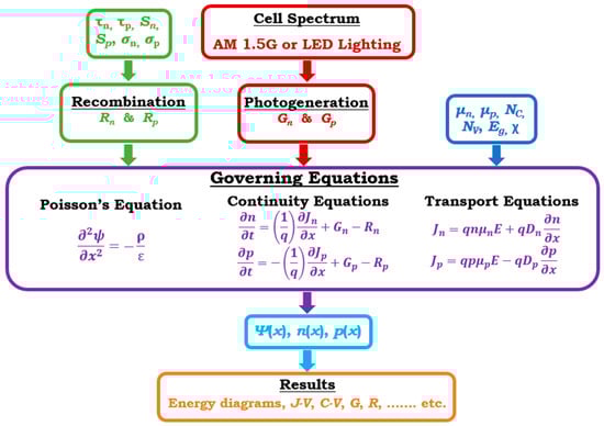
Figure 1.
SCAPS flowchart demonstrating the contained input factors and the principal semiconductor equations invoked in simulations.
The use of the SCAPS presents various advantages for solar cell design. Firstly, it allows researchers to rapidly study and compare several device architectures and materials, substantially reducing the time and cost associated with experimental effort. Additionally, the SCAPS enables detailed sensitivity analysis, providing insights into the influence of different factors on device performance and guiding optimization approaches. Trends such as current density–voltage (J-V), external quantum efficiency (EQE), and capacitance-voltage (C-V) characteristics can be obtained, which provide a comprehensive understanding of device behavior. While the SCAPS offers significant advantages in solar cell design and analysis, it is important to acknowledge its limitations. The SCAPS employs simplified mathematical and physical models to simulate solar cell behavior. While these models provide valuable insights, they may not capture all the complex phenomena occurring within real devices. While the SCAPS can handle basic optical simulations, it may not fully account for complex light interactions, such as scattering and multiple reflections, especially in structures with non-uniform or textured surfaces.
2.2. Solar Cell Configuration and Materials
The construction and energy band profile of the Se-based device are clarified in Figure 2. The Se device is based on a fabricated device that consists of FTO (as a transparent conducting front contact)/Zn0.9Mg0.1O (as an ETL)/Se (as an absorber)/MoOx (as an HTL)/Au (as a metal back contact) as displayed in Figure 2a. The presented solar cell is based on a previously fabricated Se-based cell [16]. The Se cell fabrication process included the deposition of a ZnMgO buffer layer via simultaneous RF sputtering from ZnO and MgO targets on an FTO glass substrate. The layer thickness was estimated to be 60 nm. Then, selenium film with a 100 nm thickness was deposited via thermal evaporation. Finally, the inorganic MoOx and Au back contact were deposited on the top of the Se absorber. The optimal MoOx thickness was found to be around 20 nm. More details about the processing steps and conditions as well as the electrical characterization procedures are found in [16]. Further, the energy band diagram prior to contact is illustrated in Figure 2b. The figure indicates LUMO (lowest unoccupied molecular orbital) and HOMO (highest occupied molecular orbital) energy levels. The material parameters, used in the SCAPS, are extracted from previously published resources [23,25,26,27], as listed in Table 1. Defects parameters of cell layers and at the interfaces are recorded in Table S1 (Supplementary Materials file). Specifically, the technological parameters of the initial cell are acquired from the solar cell produced using identical electron and hole transport materials [16].
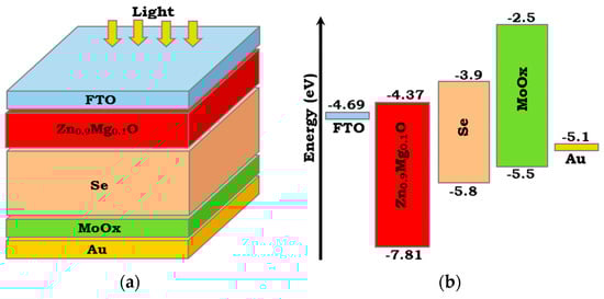
Figure 2.
FTO/ETL/Se/HTL/Au cell configuration: (a) major layers (Zn0.9Mg0.1O serves as an ETL and MoOx acts as an HTL), and (b) energy band diagram before contact clarifying the accompanying energy levels of each layer.

Table 1.
Technological factors of the distinctive layers of the Se-based device.
2.3. SCAPS Calibration
While SCAPS simulations provide valuable insights, it is essential to validate the results with experimental data. The accuracy of a simulation relies on the accuracy of the input parameters and material properties used. Experimental verification is crucial to conduct to ensure that the simulated results align with the actual device’s performance. By being aware of the limitations and using the SCAPS in conjunction with experimental validation, researchers can effectively leverage its capabilities to advance solar cell technologies.
Here, to verify the consistency of the physical models and the factors of the different materials applied in the simulation platform, the initial extracted parameters of the distinct thin films are utilized to obtain the output PV metrics. In this context, the J–V plots under standard AM1.5G illumination, obtained from both SCAPS simulation and measurements in [16], are compared, as illustrated in Figure 3a. In addition, the simulated external quantum efficiencies are also shown in Figure 3b. The main optoelectronic factors from both simulation and measurements are recorded in the inset of Figure 3a (where Jsc is the short-circuit current density, while FF represents the fill factor). As is clearly observed, the output metrics indicate a nice match between the calibrated results and measured cell parameters.
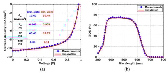
Figure 3.
Simulation model calibration versus experimental data [16]: (a) illuminated (AM1.5G) J–V curves, and (b) EQE spectra.
2.4. Impact of Indoor Light LED
Indoor light sources generally exhibit emission spectra ranging from 400 to 800 nm, featuring low intensities below 1 mW/cm2 [28], which are normally narrower and weaker than the AM 1.5G illumination spectrum. Consequently, solar cells designed for harvesting sunlight may not be optimal for indoor light circumstances. Moreover, the reaction of PV cells to indoor artificial light sources differs significantly from their response to AM 1.5 G illumination. To assess the performance of the Se PV device under the influence of indoor conditions, we employed the spectra of a white LED. Figure 4a displays the emission power at varying wavelengths, as obtained from REF [20]. A temperature of 2700 K was invoked, signifying a warm-white LED operation, where the emission peaks around 600 nm were in the orange-red part of the spectrum, gradually decreasing towards the blue part.
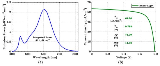
Figure 4.
(a) Emission power spectrum of a 2700 K LED at 1000 lux with 311 μW/cm2 of integrated power [20], and (b) J–V curves of a Se cell under the corresponding spectrum.
The output J–V curve of the initial Se cell was evaluated under incident LED illumination, as specified in Figure 4b. The output metrics of the cell are analyzed and highlighted in the inset of the figure. A Voc of 0.788 V was obtained, while a Jsc of 64.9 μA/cm2 was achieved. While these recorded values are less than those obtained under the illumination of AM1.5G, a significant increase in the fill factor is observed, where the FF becomes 71.39% under LED operation instead of the low value of 62.72% obtained when the device is illuminated with the standard AM1.5G spectrum. The PCE is also boosted to 11.78%, indicating the usefulness of using Se under an LED environment. In the next section, an investigation of the most effective parameters that influence cell functioning will be carried out. A proposed structure will be introduced in which a double ETL will be designed to achieve appropriate band alignment.
3. Results and Discussion
In this section, we delve into the critical factors influencing the performance of Se solar cells, focusing on different key aspects. First, the absorber’s main parameters are investigated, as indicated in Section 3.1. We explore how reducing defect density leads to longer carrier lifetimes and increased diffusion lengths, ultimately reducing recombination losses. The impact of absorber thickness on performance is analyzed, revealing the trade-off between thickness and efficiency. Moving forward, we investigate the design of the single-ETL layer in Section 3.2, particularly the importance of achieving favorable conduction band offsets and a favorable interface recombination velocity to facilitate charge extraction and minimize recombination. Then, in Section 3.3, we introduce a double-ETL configuration as a promising strategy to address performance limitations. We conclude this section by presenting the results of the final optimization steps, showcasing the significant improvements achieved via these enhancements (Section 3.4). Additionally, in Section 3.5, we explore the influence of LED temperature and absorber bandgap on cell performance, shedding light on the optimal conditions for Se cells in indoor applications. Furthermore, we provide a comprehensive comparison of our optimized cell with other cells reported in the literature, highlighting the unique contributions and potential of Se solar cells for indoor use.
3.1. Impact of Absorber Defect Density (Nt) and Thickness
Trap-assisted Shockley–Read–Hall (SRH) recombination, which is attributed to a high defect density (Nt) resulting from poor film quality, is considered to be the governing recombination mechanism in Se cells [26]. In this type of recombination mechanism, the photoexcited charge carriers recombine via trap states [29]. The SRH recombination process can be described via Equations (1) and (2) [29], where τ represents the lifetime, and Nt and Et denote the defect concentration and defect energy level, respectively. The variables σ and Vth correspond to the capture cross-section and thermal velocity.
The diffusion length (L) of carriers in the absorber film can be determined by applying Equation (3), given that D represents the diffusion coefficient, which can be calculated as .
As observed in Equations (1)–(3), a decrease in defect concentration leads to an increase in carrier lifetime. This leads to longer diffusion lengths and reduced recombination, which are crucial factors for improving cell performance. Figure 4 demonstrates that lowering the defect density results in a lower recombination rate within the Se absorber layer (Figure 5a) and improved J–V curves (Figure 5b). Additionally, Table 2 presents the change in diffusion length corresponding to different defect densities. Figure 6 shows the relationship between PCE and absorber thickness for various diffusion lengths, utilizing the values from the table.
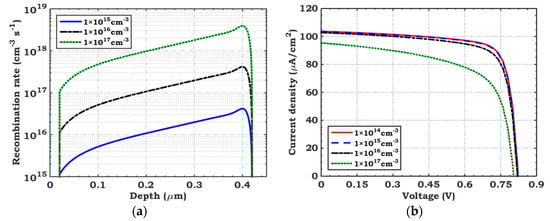
Figure 5.
Impact of varying absorber defect density on (a) recombination inside Se and (b) J–V characteristics.
Table 2.
Change in diffusion length related to change in Nt.
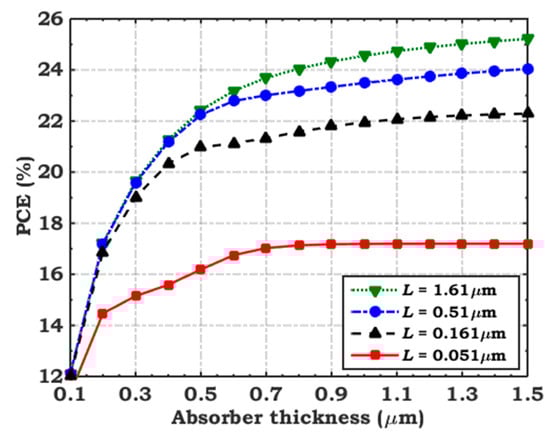
Figure 6.
Variation of PCE with absorber thickness for distinct diffusion lengths.
The figure suggests that by reducing Nt (resulting in increased L), the thickness of the absorber can be augmented to match the diffusion length, leading to enhanced absorption and higher efficiency. Considering the limited change in J–V behavior as Nt is varied from 1014 cm−3 to 1015 cm−3, the optimal Nt value is fixed at 1015 cm−3, resulting in a diffusion length of L = 0.51 μm. Based on this condition, an efficiency of up to 24% can be accomplished given an absorber film thickness of about 1.5 μm. For this reason, an absorber thickness of 300 nm, which is smaller than the chosen diffusion length (510 nm) at the specified Nt (1015 cm−3), can be selected.
3.2. Impact of CBO and Interface Recombination Velocity in Single ETL
To better understand the behavior of the initial PV device, the various current components, extracted from simulation, are drawn, as illustrated in Figure 7a. The plot depicts the total generation and recombination currents, which are found to be equal at the open-circuit condition. Additionally, the figure shows both interface and bulk current components. Observing the tendency of these currents, it becomes evident that interface recombination exceeds bulk recombination, which is undesirable as it can lead to cell degradation. To further assess this result, the energy band profile is plotted, as demonstrated in Figure 7b. Also, the Voc–T characteristics offer valuable insights into the activation energy (Ea) associated with solar cell performance. In this context, Figure 7c enables the calculation of Ea by determining Voc at T = 0 K. When Ea is less than the energy gap (Eg) of the absorber material, a cliff band offset forms. Remarkably, this cliff does not impede the movement of photo-excited electrons. However, it signifies a predominance of interface-type recombination as the primary mechanism. This form of recombination arises due to inadequate energy alignment and interface defects, significantly impacting Voc and leading to its reduction. Conversely, when Ea equals Eg, a spike band offset appears, acting as a partial barrier to the movement of photo-excited electrons. Nevertheless, if this barrier remains low enough, it facilitates normal electron transfer. This suggests that interface recombination holds less significance in this scenario, with the primary recombination mechanism being Shockley–Read–Hall (SRH) recombination within the absorber’s neutral or space charge region (SCR) [30]. To gain deeper insights into the energy band profile, a comprehensive discussion about band alignment is provided below.
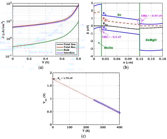
Figure 7.
(a) Different cell current components, (b) energy bands under illumination and in the short-circuit condition, and the (c) temperature-dependent Voc relation of the initial Se cell.
In the context of the studied cell, the band alignment at the ETL and absorber interface is of significant importance. The CBO at this interface is a critical parameter that affects charge recombination and carrier extraction efficiency. To enhance carrier extraction and minimize charge recombination, it is essential to achieve a favorable CBO value. As reported in previous studies [30], a CBO at the ETL–absorber interface of 0–0.3 eV results in improved performance, as it facilitates efficient carrier extraction from the absorber film to the ETL. This optimized band alignment guarantees that photogenerated electrons can easily transfer to the ETL without encountering significant energy barriers or recombination losses. Furthermore, the band alignment at the heterojunction interface between the absorber and the HTL is also important. Achieving a suitable valence band offset (VBO) is crucial to enable the efficient transport of holes from the absorber toward the HTL, thereby reducing hole recombination. By carefully engineering the band alignment at these interfaces, the challenges posed by charge recombination and extraction can be effectively tackled. It should be pointed out here that the calculation of CBO and VBO is based on the following equations [30]:
As is depicted in Figure 7b, the CBO at the Zn0.9Mg0.1O–Se interface is −0.47 eV (which represents an electron cliff), and the VBO at the MoOx–Se interface is −0.3 eV (which demonstrates a hole cliff). These alignments are not desirable in cell design as the interfaces are notorious for their severe recombination, which is primarily attributed to the cliff-like band offset [31]. In TFSCs, the preference is usually for flat bands or a slight spike-like profile [32]. Based on the previous results, it is thus evident that band alignment poses a significant issue in the initial Se solar cell for practical, specifically indoor, applications.
The following theoretical study involves varying the electron affinity (which directly changes the CBO) along with the recombination velocity (S) at the ETL–absorber interface. The aim is to identify the optimum values of the CBO and S, which play a critical function in establishing the efficiency and functionality of the cell. By systematically exploring these variations, valuable insights can be gained to enhance cell performance and address any potential issues related to charge transport and recombination processes within the device. Figure 8 illustrates the relationship between the PCE and the change in CBO at various recombination velocities. The recombination velocity ranges from 103 to 107 cm/s, while the CBO varies from −0.7 to 0.2 eV. Furthermore, Figure S1 (see the Supplementary Materials file) depicts contour graphs illustrating the dependence of cell performance metrics on both CBO and S. As anticipated, increasing the recombination velocity at a fixed CBO leads to a degradation in PCE due to the growth in surface carrier recombination. Conversely, upon varying the CBO while S remains unchanged, the PCE exhibits a consistent trend across different recombination velocities. The PCE reaches saturation within the range of −0.5 to −0.2 eV CBO values. Outside of this range, it gradually improves with lower CBO values and significantly declines with CBO values exceeding −0.2 eV. This decline can be attributed to the rising front carrier barrier associated with raising the CBO.
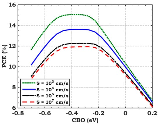
Figure 8.
Variation of PCE with CBO at different surface recombination velocities (S).
It is found that the design of the VBO in this n-i-p structure is less crucial than that in the CBO case. The results of this fact are demonstrated in Figure S2 (see the Supplementary Materials file). The maximum PCE is achieved when the VBO falls within the range of −0.3 to −0.1 eV. Beyond this range, the PCE starts to gradually decline. Moreover, the PCE decreases significantly when the VBO values exceed −0.3 eV. As mentioned herein, the VBO at the MoOx–Se interface is −0.3 eV, which is the optimum value. Thus, there is no need to engineer the VBO for this designed cell.
To engineer band alignment at the interface, the ternary compound Zn1−xMgxO is employed with x = 6, 18, 26, and 30% as an ETL. The variation in Eg and the electron affinity (χ) of Zn1−xMgxO with Mg content were obtained from the relevant literature [27], as demonstrated in Figure S3 (see the Supplementary Materials file). Additionally, the material parameters, used in the SCAPS, are extracted from previously published resources [23,27], as listed in Table S2. Figure 9 exhibits a comparison of the illuminated J–V curves for Se cells employing different x compositions. The corresponding output factors are recorded in Table 2. According to the simulation results, Zn1−xMgxO with x = 10 and 18% is identified as the most suitable ETL material due to its predicted CBOs of −0.47 and −0.31 eV, respectively. However, it is important to consider the majority barrier height between the ETL and the FTO electrode, which likewise significantly influences performance. Therefore, Table 3 presents both the CBO values and the majority barrier height (ΦF), specifically for electron transport, for the diverse ETL materials. It is noted that the S-shaped behavior in the J–V curves arises from the band misalignment between the ETL and the FTO electrode, which is influenced by the value of ΦF. This misalignment leads to an electric field that restricts electron transport to the electrode, causing the observed kink behavior. Among the materials tested, Zn0.85Mg0.15O exhibits the highest ΦF, which contributes to the distinctive S-shaped appearance.
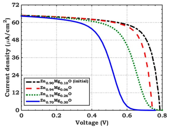
Figure 9.
Comparison of illuminated J–V characteristics between initial cell and cell with three different ETLs.
Table 3.
Comparison between the optoelectronic PV parameters utilizing Zn1−xMgxO with different x composition.
3.3. Proposed Double-ETL Configuration
Advancing charge collection and separation is a highly advantageous approach for improving solar cell performance. In this context, the ETL holds significant importance, as mentioned herein. In order to address the challenges mentioned earlier, the concept of a double ETL has been explored. This methodology involves utilizing two different materials as an alternative to a single ETL. The aim is to alleviate the limitations observed in traditional single-ETL designs. Several experimental studies have been carried out focusing on the application of double-ETL structures to boost the efficiency and stability of PV cells [33,34,35,36,37,38]. By utilizing two distinct materials in the ETL, the aim is to optimize charge transport and reduce recombination losses, thereby achieving better overall performance and paving the way for more efficient solar cell technologies.
In this part, we examine the integration of a double-ETL structure consisting of Zn0.74Mg0.26O (measuring 20 nm in thickness) as an adjacent layer to the FTO, along with a Zn0.74Mg0.26O layer measuring 60 nm in thickness. Figure 10a displays a comparison of the J–V curves under illumination for the initial Se cell and the Se cell employing the Zn0.94Mg0.06O/Zn0.74Mg0.26O double-ETL configuration. As can be noticed, the energy difference between the LUMO level of the second ETL (Zn0.74Mg0.26O) and that of the absorber is tuned to be low enough (CBO = −0.08 eV) to facilitate electron injection, as shown in Figure 10b compared to Figure 7b. Additionally, the difference between the FTO work function and the LUMO level of the first ETL (Zn0.94Mg0.06O) is well designed (ΦF = 0.25 eV). The output metrics, in this case, are as follows: Jsc = 65.63 μA/cm2, Voc = 0.9 V, FF = 71.49%, and PCE = 13.63%. Thus, the double-ETL design can improve cell performance and provide higher efficiency. The utilization of Zn0.94Mg0.06O/Zn0.74Mg0.26O as a double ETL in the presented cell leads to a significant percentage increase of approximately 15.70% compared to that of the initial Se cell.
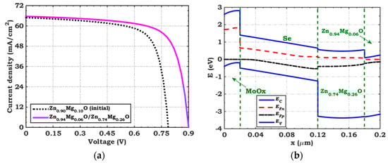
Figure 10.
(a) Comparison of illuminated J–V between the initial Se cell with a single ETL and double ETL, and (b) an energy band diagram under illumination and the short-circuit condition of the Se cell with a double ETL.
3.4. Final Optimization
Finally, according to the results presented in Section 3.1, Section 3.2 and Section 3.3, device optimizations are conducted. The simulations are repeated using the optimal values for each parameter. Table 4 summarizes the optimal value for each parameter alongside the corresponding cell performance for each scenario. Furthermore, Figure 11 illustrates the PCE at each optimization step and the percentage improvement achieved via each optimized step compared to that in the initial state. The results highlight the optimization of absorber thickness and defect density as the most significant factors, leading to a 66.30% enhancement in a relative percentage. This underscores the importance of trap state passivation in reducing the defect density and its negative impact on cell performance. In addition, Figure 12 showcases the J-V and EQE characteristics of the initial and final optimized Se cells. The notable improvement in cell performance can be credited to the cumulative effect of the optimization steps, resulting in a maximum PCE of 26.93% and a relative percentage improvement of 128.61% compared to that of the initial Se cell. It should be highlighted here that there is still ample room for further enhancements, including addressing issues such as series resistance, optimizing back contacts, managing interface traps, and various other aspects that can contribute to refining and improving efficiency to reach the ideal S-Q limit.
Table 4.
Evaluation of performance metrics for the Se cell across different optimization stages.
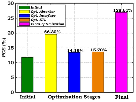
Figure 11.
PCE variation for various optimization scenarios of the Se cell, showing the relative percentage enhancements in calculated efficiency.
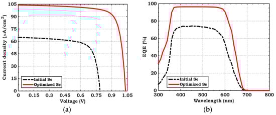
Figure 12.
A comparison between (a) J–V under illumination and (b) EQE spectra of initial and final optimized Se cells.
3.5. Impact of LED Temperature and Bandgap on Cell Performance
This subsection presents the simulation results concerning the behavior of the initial Se cell under distinctive conditions. The influence of the indoor white LED light’s color temperature and that of the absorber bandgap on the PV metrics of the cell are simultaneously examined. The spectra of white LEDs used in the study comprise an intense blue emission. The illuminance of the incident LED light can be amended within the range of 200 to 10,000 lux, corresponding to an intensity range of 57.9–2895 µW/cm2 [28]. Extracted from [28], Figure 13 showcases the relationship between wavelength and photon flux for incident LED light sources of different color temperatures. A color temperature of 7500 K represents a cool white LED, where the photon flux is at its maximum at about 450 nm. For a color temperature of 5300 K, there is a slight additional maximum point around 630 nm. A warm-white LED with a temperature of 2900 K shows a maximum photon flux of around 630 nm.
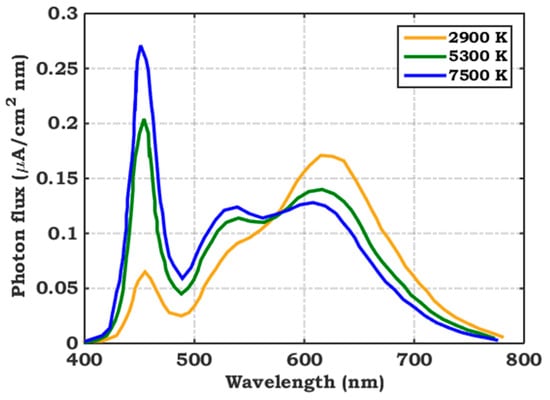
Figure 13.
The variation in the photon flux of white LEDs as a function of wavelength at various temperatures, extracted from [28].
It is well known that the energy band depends strongly on the fabrication process of Se films [39,40]. Thus, we explored the influence of changing the bandgap of the absorber from 1.75 to 2 eV on the performance metrics of the cell. The simulation results are demonstrated in Figure 14. It can be observed from Figure 14a that the behavior of Jsc shows an enhancement with increasing temperature, while it declines with an increase in the absorber bandgap. This can be attributed to the fact that the lower-bandgap absorber has higher potential for capturing photons originating from the extended wavelength region of the visible spectrum, which is in excellent agreement with the spectral characteristics of the white LED spectrum (as shown in Figure 13).
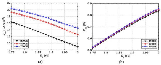
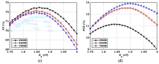
Figure 14.
The dependence of cell output parameters on the absorber bandgap at different color temperatures of indoor white LED: (a) Jsc, (b) Voc, (c) FF, and (d) PCE.
In terms of the trend observed for Voc (as shown in Figure 14b), it was found to be nearly unaffected by the color temperature, while its values exhibited an increase with an increase in the absorber bandgap, as expected. Conversely, the FF (depicted in Figure 14c) showed a decrease with an increase in the color temperature, while keeping the bandgap fixed. Finally, as demonstrated in Figure 14d, a noticeable variation in PCE is observed. The PCE showed an increase with an increase in the color temperature. Moreover, the optimal bandgap differs for warm (2900 K) and cool (7500 K) LED bulbs. The optimal bandgap for warm light is determined to be 1.85 eV, while for cool light, it is 1.9 eV [10].
In the final analysis, we present a comprehensive comparison between our optimized cell and other cells reported in the literature. Table 5 provides a detailed overview of these cells, highlighting some of their characteristics and performance metrics. It is worth emphasizing that the cells listed in the table encompass a mix of experimentally fabricated cells and cells simulated using numerical methods. This comparison serves to provide valuable insights into the performance of our optimized cell relative to that of other existing candidates in the field. While there have been several endeavors to investigate perovskite and organic materials for indoor applications, limited research has focused on Se solar cells. In a recent study [20], the efficiency of Se cells was successfully optimized by adjusting the coverage of the Te adhesion layer. This optimization led to a remarkable efficiency of 15.1% under 1000 lux indoor LED illumination, and the cells demonstrated long-term stability without efficiency loss after continuous indoor illumination for 1000 h, even without the use of encapsulation [20]. To the best of our knowledge, this study presents an initial attempt to simulate the behavior of Se solar cells under white LED illumination. Previous research efforts in simulating wide-bandgap solar cells for indoor use have been scarce. One notable simulation study focused on all-polymer solar cells [11], as summarized in Table 5.
Table 5.
A state-of-the-art comparison between different technological and output parameters of Se and other perovskite and organic cells.
4. Conclusions
This paper presented the outcomes of simulations conducted on a selenium (Se)-based solar cell, which harnesses photon energy emanating from indoor light-emitting diodes (LEDs) through the utilization of the SCAPS-1D device. Firstly, the validity of our simulation model, within the SCAPS, was established by comparing the output characteristics with those of an earlier-manufactured solar cell with a FTO/ZnMgO/Se/MoOx/Au configuration, achieving a PCE of 6.41% in the AM1.5G spectrum, in accordance with the experimental value of 6.51%. Moving forward, an assessment of the PV device‘s performance was carried out under the spectra of an artificial white LED. Remarkably, the utilization of Se in an LED environment elevated the PCE to 11.78%.
The enhancement of cell performance was achieved through meticulous design adjustments to the absorber’s key parameters, including to thickness and defect density. Additionally, optimization of the CBO and interface recombination velocity between the ETL and the Se absorber demonstrated a vital role. To further improve band alignment between device layers, we introduced a double-ETL structure. Through these optimization processes, a significant advancement in cell performance was attained, resulting in a remarkable maximum PCE of 26.93% under LED illumination at 311 μW/cm2.
Furthermore, we delved into the influence of LED temperature and absorber bandgap on cell performance, providing insights into the optimal conditions for Se cells in indoor applications. The findings presented in this study not only contribute to evaluating the potential of Se solar cells as indoor photovoltaics but also propose a tailored approach for designing indoor applications.
Supplementary Materials
The following supporting information can be downloaded at https://www.mdpi.com/article/10.3390/cryst13121668/s1. Figure S1: Contour graphs of cell performance figure of merit dependency on conduction band offset (CBO) and surface recombination velocity (S); Figure S2: A theoretical study for PCE and back barrier height (ΦB) dependency on VBO of HTL layer.; Figure S3: Variation in Eg and χ of Zn1-xMgxO depending on the variation of Mg content; Table S1: Defects parameters of cell layers and at the interfaces; Table S2: Basic parameters of Zn1−xMgxO with x = 6, 15, 18, 30% [24,45].
Author Contributions
S.M.H.Q.: writing—review and editing, validation, methodology, and resources. A.S.: writing—review and editing, software, methodology, and conceptualization. M.O.: writing—review and editing, software, validation, and methodology. C.G.: validation, methodology, and supervision. M.A.: visualization, validation, methodology, and investigation. H.M.G.: visualization, validation, methodology, and investigation. M.M.S.: writing—review and editing, software, and validation. All authors have read and agreed to the published version of the manuscript.
Funding
This research was funded by the Researchers supporting project number (RSPD2023R762), King Saud University, Riyadh, Saudi Arabia.
Data Availability Statement
The data presented in this study is available in the article.
Conflicts of Interest
The authors declare that they have no known competing financial interest or personal relationship that could have appeared to influence the work reported in this paper.
References
- Zekry, A. A road map for transformation from conventional to photovoltaic energy generation and its challenges. J. King Saud Univ.-Eng. Sci. 2020, 32, 407–410. [Google Scholar] [CrossRef]
- Green, M.A. Solar Cells: Operating Principles, Technology, and System Applications; Prentice-Hall, Inc.: Englewood Cliffs, NJ, USA, 1982; 288p. [Google Scholar]
- Salem, M.S.; Shaker, A.; Almurayziq, T.S.; Alshammari, M.T. Prospective efficiency boosting of full-inorganic single-junction Sb2(S, Se)3 solar cell, Sol. Energy Mater. Sol. Cells 2022, 248, 112001. [Google Scholar] [CrossRef]
- Mishra, S.; Ghosh, S.; Boro, B.; Kumar, D.; Porwal, S.; Paul, M.; Dixit, H.; Singh, T. Solution-processed next generation thin film solar cells for indoor light application. Energy Adv. 2022, 1, 761–792. [Google Scholar] [CrossRef]
- Biswas, S.; Kim, H. Solar Cells for Indoor Applications: Progress and Development. Polymers 2020, 12, 1338. [Google Scholar] [CrossRef]
- Sivaraj, S.; Rathanasamy, R.; Kaliyannan, G.V.; Panchal, H.; Alrubaie, A.J.; Jaber, M.M.; Said, Z.; Memon, S. A Comprehensive Review on Current Performance, Challenges and Progress in Thin-Film Solar Cells. Energies 2022, 15, 8688. [Google Scholar] [CrossRef]
- Dhilipan, J.; Vijayalakshmi, N.; Shanmugam, D.B.; Ganesh, R.J.; Kodeeswaran, S.; Muralidharan, S. Performance and efficiency of different types of solar cell material—A review. Mater. Today Proc. 2022, 66, 1295–1302. [Google Scholar] [CrossRef]
- De Rossi, F.; Pontecorvo, T.; Brown, T.M. Characterization of photovoltaic devices for indoor light harvesting and customization of flexible dye solar cells to deliver superior efficiency under artificial lighting. Appl. Energy 2015, 156, 413–422. [Google Scholar] [CrossRef]
- Reynaud, C.A.; Clerc, R.; Lechêne, P.B.; Hébert, M.; Cazier, A.; Arias, A.C. Evaluation of indoor photovoltaic power production under directional and diffuse lighting conditions. Sol. Energy Mater. Sol. Cells 2019, 200, 110010. [Google Scholar] [CrossRef]
- Jarosz, G.; Marczyński, R.; Signerski, R. Effect of band gap on power conversion efficiency of single-junction semiconductor photovoltaic cells under white light phosphor-based LED illumination. Mater. Sci. Semicond. Process. 2020, 107, 104812. [Google Scholar] [CrossRef]
- Alanazi, T.I. TCAD Device Simulation of All-Polymer Solar Cells for Indoor Applications: Potential for Tandem vs. Single Junction Cells. Polymers 2023, 15, 2217. [Google Scholar] [CrossRef]
- Qaid, S.M.H.; Shaker, A.; Okil, M.; Alkadi, M.; Ahmed, A.A.A.; Zein, W. Optimizing CBTSSe solar cells for indoor applications through numerical simulation. Opt. Quantum Electron. 2023, 55, 1245. [Google Scholar] [CrossRef]
- Juang, S.S.-Y.; Lin, P.-Y.; Lin, Y.-C.; Chen, Y.-S.; Shen, P.-S.; Guo, Y.-L.; Wu, Y.-C.; Chen, P. Energy Harvesting Under Dim-Light Condition with Dye-Sensitized and Perovskite Solar Cells. Front. Chem. 2019, 7, 209. [Google Scholar] [CrossRef] [PubMed]
- Fritts, C.E. On a new form of selenium cell, and some electrical discoveries made by its use. Am. J. Sci. 1883, 26, 465–472. [Google Scholar] [CrossRef]
- Nakada, T.; Kunioka, A. Polycrystalline Thin-Film TiO2 /Se Solar Cells. Jpn. J. Appl. Phys. 1985, 24, L536. [Google Scholar] [CrossRef]
- Todorov, T.K.; Singh, S.; Bishop, D.M.; Gunawan, O.; Lee, Y.S.; Gershon, T.S.; Brew, K.W.; Antunez, P.D.; Haight, R. Ultrathin high band gap solar cells with improved efficiencies from the world’s oldest photovoltaic material. Nat. Commun. 2017, 8, 682. [Google Scholar] [CrossRef]
- Hadar, I.; Song, T.-B.; Ke, W.; Kanatzidis, M.G. Modern processing and insights on selenium solar cells: The world’s first photovoltaic device. Adv. Energy Mater. 2019, 9, 1802766. [Google Scholar] [CrossRef]
- Fu, L.; Zheng, J.; Yang, X.; He, Y.; Chen, C.; Li, K.; Tang, J. Rapid thermal annealing process for Se thin-film solar cells. Faraday Discuss. 2022, 239, 317–327. [Google Scholar] [CrossRef]
- Kawagishi, T.; Adachi, Y.; Kobayashi, T. Photovoltaic performances of TiO2/Se heterojunction devices with different crystallographic structures of sputter-deposited TiO2 thin films. Mater. Chem. Phys. 2023, 297, 127371. [Google Scholar] [CrossRef]
- Yan, B.; Liu, X.; Lu, W.; Feng, M.; Yan, H.J.; Li, Z.; Liu, S.; Wang, C.; Hu, J.S.; Xue, D.J. Indoor photovoltaics awaken the world’s first solar cells. Sci. Adv. 2022, 8, eadc9923. [Google Scholar] [CrossRef]
- Müller, M.F.; Freunek, M.; Reindl, L.M. Maximum efficiencies of indoor photovoltaic devices. IEEE J. Photovolt. 2013, 3, 59–64. [Google Scholar] [CrossRef]
- Youngman, T.H.; Nielsen, R.; Crovetto, A.; Seger, B.; Hansen, O.; Chorkendorff, I.; Vesborg, P.C.K. Semitransparent Selenium Solar Cells as a Top Cell for Tandem Photovoltaics. Sol. RRL 2021, 5, 2100111. [Google Scholar] [CrossRef]
- Salem, M.S.; Shaker, A.; Othman, M.S.; Al-Bagawia, A.H.; Fedawy, M.; Aleid, G.M. Numerical analysis and design of high performance HTL-free antimony sulfide solar cells by SCAPS-1D. Opt. Mater. 2022, 123, 111880. [Google Scholar] [CrossRef]
- Gamal, N.; Sedky, S.H.; Shaker, A.; Fedawy, M. Design of lead-free perovskite solar cell using Zn1−xMgxO as ETL: SCAPS device simulation. Optik 2021, 242, 167306. [Google Scholar] [CrossRef]
- Jannat, F.; Ahmed, S.; Alim, M.A. Performance analysis of cesium formamidinium lead mixed halide based perovskite solar cell with MoOx as hole transport material via SCAPS-1D. Optik 2021, 228, 166202. [Google Scholar] [CrossRef]
- Youngman, T.H. Wide-Bandgap Selenium-Based Solar Cells for Tandem Device Applications, Department of Physics; Technical University of Denmark: Kongens Lyngby, Denmark, 2021. [Google Scholar]
- He, X.; Wu, L.; Hao, X.; Zhang, J.; Li, C.; Wang, W.; Feng, L.; Du, Z. The Band Structures of Zn1−xMgxO(In) and the Simulation of CdTe Solar Cells with a Zn1−xMgxO(In) Window Layer by SCAPS. Energies 2019, 12, 291. [Google Scholar] [CrossRef]
- Cui, Y.; Wang, Y.; Bergqvist, J.; Yao, H.; Xu, Y.; Gao, B.; Yang, C.; Zhang, S.; Inganäs, O.; Gao, F.; et al. Wide-gap non-fullerene acceptor enabling high-performance organic photovoltaic cells for indoor applications. Nat. Energy 2019, 4, 768–775. [Google Scholar] [CrossRef]
- Kirchartz, T. Generalized Detailed Balance Theory of Solar Cells; Forschungszentrum Jülich: Jülich, Germany, 2009. [Google Scholar]
- Minemoto, T.; Murata, M. Theoretical analysis on effect of band offsets in perovskite solar cells. Sol. Energy Mater. Sol. Cells 2015, 133, 8–14. [Google Scholar] [CrossRef]
- Scheer, R.; Schock, H.W. Chalcogenide Photovoltaics: Physics, Technologies, and Thin Film Devices; John Wiley & Sons: Hoboken, NJ, USA, 2011. [Google Scholar] [CrossRef]
- Chen, C.; Liu, X.; Li, K.; Lu, S.; Wang, S.; Li, S.; Lu, Y.; He, J.; Zheng, J.; Lin, X.; et al. High-efficient Sb2Se3 solar cell using ZnxCd1−xS n-type layer. Appl. Phys. Lett. 2021, 118, 172103. [Google Scholar] [CrossRef]
- Yi, H.; Wang, D.; Mahmud, M.A.; Haque, F.; Upama, M.B.; Xu, C.; Duan, L.; Uddin, A. Bilayer SnO2 as Electron Transport Layer for Highly Efficient Perovskite Solar Cells. ACS Appl. Energy Mater. 2018, 1, 6027–6039. [Google Scholar] [CrossRef]
- Pitchaiya, S.; Eswaramoorthy, N.; Natarajan, M.; Santhanam, A.; Ramakrishnan, V.M.; Asokan, V.; Palanichamy, P.; Palanisamy, B.; Kalimuthu, A.; Velauthapillai, D. Interfacing green synthesized flake like-ZnO with TiO2 for bilayer electron extraction in perovskite solar cells. New J. Chem. 2020, 44, 8422–8433. [Google Scholar] [CrossRef]
- Li, N.; Yan, J.; Ai, Y.; Jiang, E.; Lin, L.; Shou, C.; Yan, B.; Sheng, J.; Ye, J. A low-temperature TiO2/SnO2 electron transport layer for high-performance planar perovskite solar cells. Sci. China Mater. 2020, 63, 207–215. [Google Scholar] [CrossRef]
- Otoufi, M.K.; Ranjbar, M.; Kermanpur, A.; Taghavinia, N.; Minbashi, M.; Forouzandeh, M.; Ebadi, F. Enhanced performance of planar perovskite solar cells using TiO2/SnO2 and TiO2/WO3 bilayer structures: Roles of the interfacial layers. Sol. Energy 2020, 208, 697–707. [Google Scholar] [CrossRef]
- Zhao, Y.; Li, C.; Niu, J.; Zhi, Z.; Chen, G.; Gong, J.; Li, J.; Xiao, X. Zinc-based electron transport materials for over 9.6%-efficient S-rich Sb2(S, Se)3 solar cells. J. Mater. Chem. A 2021, 9, 12644–12651. [Google Scholar] [CrossRef]
- Lachore, W.L.; Andoshe, D.M.; Mekonnen, M.A.; Hone, F.G. Recent progress in electron transport bilayer for efficient and low-cost perovskite solar cells: A review. J. Solid State Electrochem. 2022, 26, 295–311. [Google Scholar] [CrossRef]
- Tutihasi, S.; Chen, I. Optical properties and band structure of trigonal selenium. Phys. Rev. 1967, 158, 623–630. [Google Scholar] [CrossRef]
- Bhatnagar, A.K.; Reddy, K.V.; Srivastava, V. Optical energy gap of amorphous selenium: Effect of annealing. J. Phys. D. Appl. Phys. 1985, 18, L149. [Google Scholar] [CrossRef]
- Cui, Y.; Hong, L.; Zhang, T.; Meng, H.; Yan, H.; Gao, F.; Hou, J. Accurate photovoltaic measurement of organic cells for indoor applications. Joule 2021, 5, 1016–1023. [Google Scholar] [CrossRef]
- You, Y.; Song, C.E.; Hoang, Q.V.; Kang, Y.; Goo, J.S.; Ko, D.; Lee, J.; Shin, W.S.; Shim, J.W. Highly Efficient Indoor Organic Photovoltaics with Spectrally Matched Fluorinated Phenylene-Alkoxybenzothiadiazole-Based Wide Bandgap Polymers. Adv. Funct. Mater. 2019, 29, 1901171. [Google Scholar] [CrossRef]
- Castro-Hermosa, S.; Lucarelli, G.; Top, M.; Fahland, M.; Fahlteich, J.; Brown, T.M. Perovskite Photovoltaics on Roll-to-Roll Coated Ultra-thin Glass as Flexible High-Efficiency Indoor Power Generators. Cell Reports Phys. Sci. 2020, 1, 100045. [Google Scholar] [CrossRef]
- Peng, Y.; Huq, T.N.; Mei, J.; Portilla, L.; Jagt, R.A.; Occhipinti, L.G.; MacManus-Driscoll, J.L.; Hoye, R.L.Z.; Pecunia, V. Lead-Free Perovskite-Inspired Absorbers for Indoor Photovoltaics. Adv. Energy Mater. 2021, 11, 2002761. [Google Scholar] [CrossRef]
- Salem, M.S.; Shaker, A.; Abouelatta, M.; Alanazi, A.; Al-Dhlan, K.A.; Almurayziq, T.S. Numerical analysis of hole transport layer-free antimony selenide solar cells: Possible routes for efficiency promotion. Opt. Mater. (Amst). 2022, 129, 112473. [Google Scholar] [CrossRef]
Disclaimer/Publisher’s Note: The statements, opinions and data contained in all publications are solely those of the individual author(s) and contributor(s) and not of MDPI and/or the editor(s). MDPI and/or the editor(s) disclaim responsibility for any injury to people or property resulting from any ideas, methods, instructions or products referred to in the content. |
© 2023 by the authors. Licensee MDPI, Basel, Switzerland. This article is an open access article distributed under the terms and conditions of the Creative Commons Attribution (CC BY) license (https://creativecommons.org/licenses/by/4.0/).