Article

Effect of Plasma Etching Depth on Subsurface Defects in Quartz Crystal Elements

Rsearch Centre of Laser Fusion, China Academy of Engineering Physics, Mianyang 621900, China
*
Author to whom correspondence should be addressed.
These authors contributed equally to this work.
Crystals 2023, 13(10), 1477; https://doi.org/10.3390/cryst13101477
Submission received: 7 September 2023 / Revised: 18 September 2023 / Accepted: 24 September 2023 / Published: 11 October 2023

Abstract

:
After the plasma etching of quartz crystal, the crystal lattice underwent changes in response to the length of plasma etching time. The lattice arrangement of quartz crystal was the most orderly after plasma etching for 1000 nm, and with the increase in etching time, the lattice arrangement became less orderly again. The weak absorption value of quartz crystal was also consistent with this conclusion. In this paper, we investigated the effect of lattice changes on the damage threshold of quartz crystals by characterizing the quartz crystals using Reactive Ion Etching (RIE). We also examined the effect of lattice variation on roughness and surface topography.

1. Introduction

Transmissive optics are a common component in large scientific devices and complex optical systems. In high-power and high-energy laser systems, such as the NIF (National Ignition Facility) device in the United States and the LMJ device in France, the energy carried by reflected light can cause catastrophic damage to the optical elements [1,2,3,4]. To address this issue, researchers have improved the damage threshold of optical components in previous studies by improving their processing or by treating damage precursors [5,6,7,8,9].
Quartz materials are commonly used as lenses due to their good optical transmittance in the ultraviolet to near-infrared wavelength bands. To improve the damage threshold of quartz materials, three aspects can be considered. Firstly, the processing and polishing of the quartz material can be improved. Currently, airbag polishing, magnetorheological polishing, and other methods are used to polish the surface of fused silica optical elements to improve their damage threshold [10,11,12]. Secondly, surface and sub-surface defects of quartz materials can be treated after polishing. Damage precursors of optical elements are mainly treated using dry etching, wet etching, and composite etching to improve the damage threshold [13,14,15]. Finally, from an optical perspective, dry etching can be used to form a sub-wavelength structure on the surface of quartz material to regulate the incident light field and enhance the transmittance of the optical element, thereby improving the overall damage threshold of the optical element [16,17,18,19]. Current research focuses mainly on eliminating damage precursors of optical elements in the ultraviolet wavelength band.
Larry D. Merkle et al. investigated the body damage of quartz crystals and fused silica under 1064 nm and 532 nm laser irradiation in 1983 but did not study the relationship between damage precursors and damage. In 2019, Taixiang Liu et al. etched fused silica optics using HF and simulated the results using FDTD, demonstrating that HF can passivate surface and subsurface cracks, thereby improving the damage threshold. In 2020, Jianda Shao’s team from the Shanghai Institute of Optical Machinery (SIOM) improved the threshold of fused silica defects by 33% compared to the CMP(Chemical Mechanical Polishing) polishing process by using chemical etching and CO2 laser. Xiangxu Chai et al. studied the relationship between large aperture LID growth in fused silica lenses at 351 nm in 2021, and the results showed that the damage was mainly caused by indicated defects. In 2021, Feng Shi et al. from National Defense University investigated the KOH-based wet etching technique to inhibit damage precursors of fused silica materials, and the results showed that KOH-based etching ensured the indicated roughness of fused silica optical elements and reduced impurities. In 2022, Bo Li proposed a method of large-incidence-angle ion-beam etching followed by HF etching to remove metallic impurities and sub-surface defects indicated by fused silica and to prepare fused silica optical elements with a higher degree of faceted shape. In 2023, Dinghuai Yang et al. investigated the origins of point defects, their evolutionary patterns, and their relationship with damage. They identified seven types of point defects caused by atomic-scale strong laser irradiation, which provided a new idea for defect-induced damage in optical elements [20,21,22,23,24,25,26]. Previous studies have shown that researchers focus primarily on removing damage precursors from the surface and subsurface of optical elements using dry etching versus wet etching techniques. However, it has not been investigated whether the lattice structure of optical elements can be damaged during the dry etching process. In this study, we investigated the relationship between the cell changes of quartz crystals and their own roughness before and after etching. We also combined this information with the final damage threshold test to study the migration from quartz crystal materials to fused silica materials. Our findings provide important insights into the removal of damage precursors from optical components and the improvement of the damage threshold.
This study focuses on quartz crystal optical elements. Reactive ion etching technology was used to etch and remove surface and sub-surface defects of quartz crystals. The defects of different degrees of quartz crystal etching were characterized and detected using white light interference imaging and photothermal weak absorption testing techniques. The lattice of quartz crystals before and after etching was tested by X-ray diffraction. The results show that RIE etching is an effective method to remove surface and subsurface defects from quartz crystals. The choice of the depth of ion etching has an important effect on the lattice changes of quartz crystals, and the etching modifies the crystal cells well, reducing the roughness and weak photothermal absorption values of the samples. Choosing the right etching depth for quartz crystal optics can greatly improve their damage threshold.

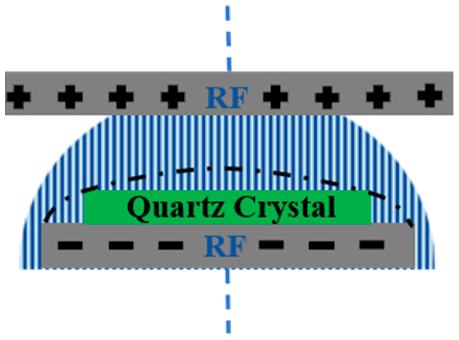
2. Experimental Section

Five quartz crystals with a 50 mm side length and 5 mm thickness were purchased from Oerlite. The processed surface was perpendicular to the optical axis with a roughness below 1 nm. RIE etching was performed using a gas mixture of CHF3 and Ar, with an RF source power of 200 W, a working pressure of 20 mtorr for the gas mixture, and a flow rate of CHF3:72sccm and Ar:5sccm. The calibrated etching rate was 2.14 µm/h. The five quartz crystal elements were subjected to RIE with an etching depth determined according to the etching time [27], as illustrated in Figure 1. The etching depths were 0, 100 nm, 500 nm, 1000 nm, and 5000 nm, respectively, as shown in Table 1.

3. Results and Discussion

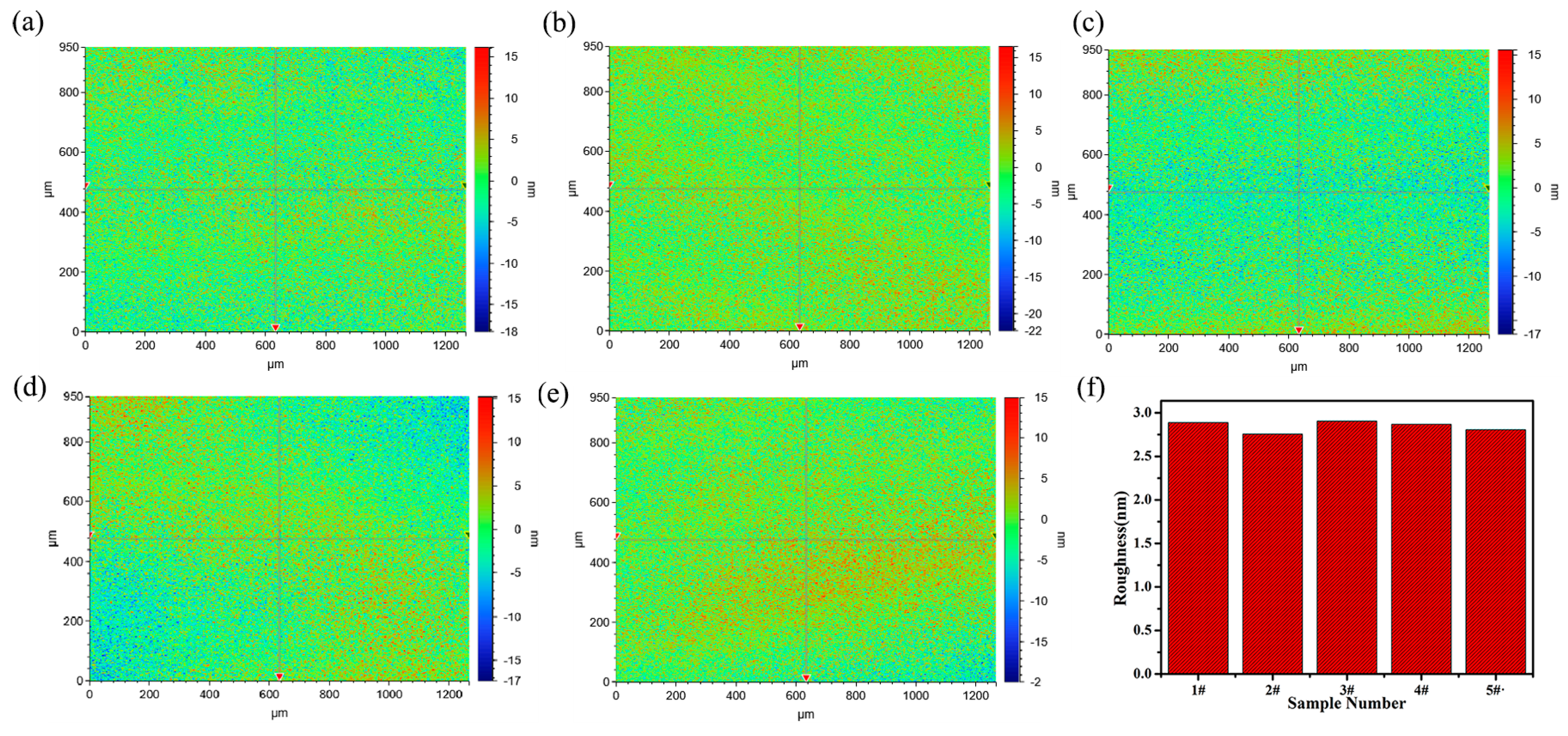
3.1. Surface Roughness Analysis

Figure 2 shows the surface morphology of the etched samples, which were examined using a white light interferometer. The testing process involved using the white light interference principle to obtain the value of roughness of the optical element surface by recording the position information of 307,200 points in a certain area of the sample surface and counting these points through software processing. To ensure the rigor of this study, we chose quartz crystals with a uniform polishing batch (the same process, the same equipment) and made provisions for the roughness of the face shape of the polished samples, with roughness errors less than ± 0.5 nm. The test morphology is shown in Figure 2a–e. Figure 2f shows that, statistically, the roughness of the sample surface decreases, then increases, and then decreases with the increase in the etching depth. This is mainly due to the fact that when the etching depth reaches 100 nm, the processing defects on the surface of the quartz crystal are removed. When the etching depth is increased to 500 nm, process cracks or dislocations on the subsurface caused by the process are exposed, resulting in an increase in the surface roughness of the sample. As the etching depth is increased to 1000 nm, the subsurface defects are removed from the sample, resulting in a decrease in roughness. However, when the etching depth is increased to 5000 nm, sub-wavelength structural etching occurs, which changes the optical properties of the quartz crystal and may deposit some impurities, such as etching reactants, on the sample. Therefore, the results of the white light interference test suggest that selecting an etching depth of 1000 nm can effectively remove the surface and sub-surface defects of the quartz crystal after processing and reduce the roughness of the sample [28,29].

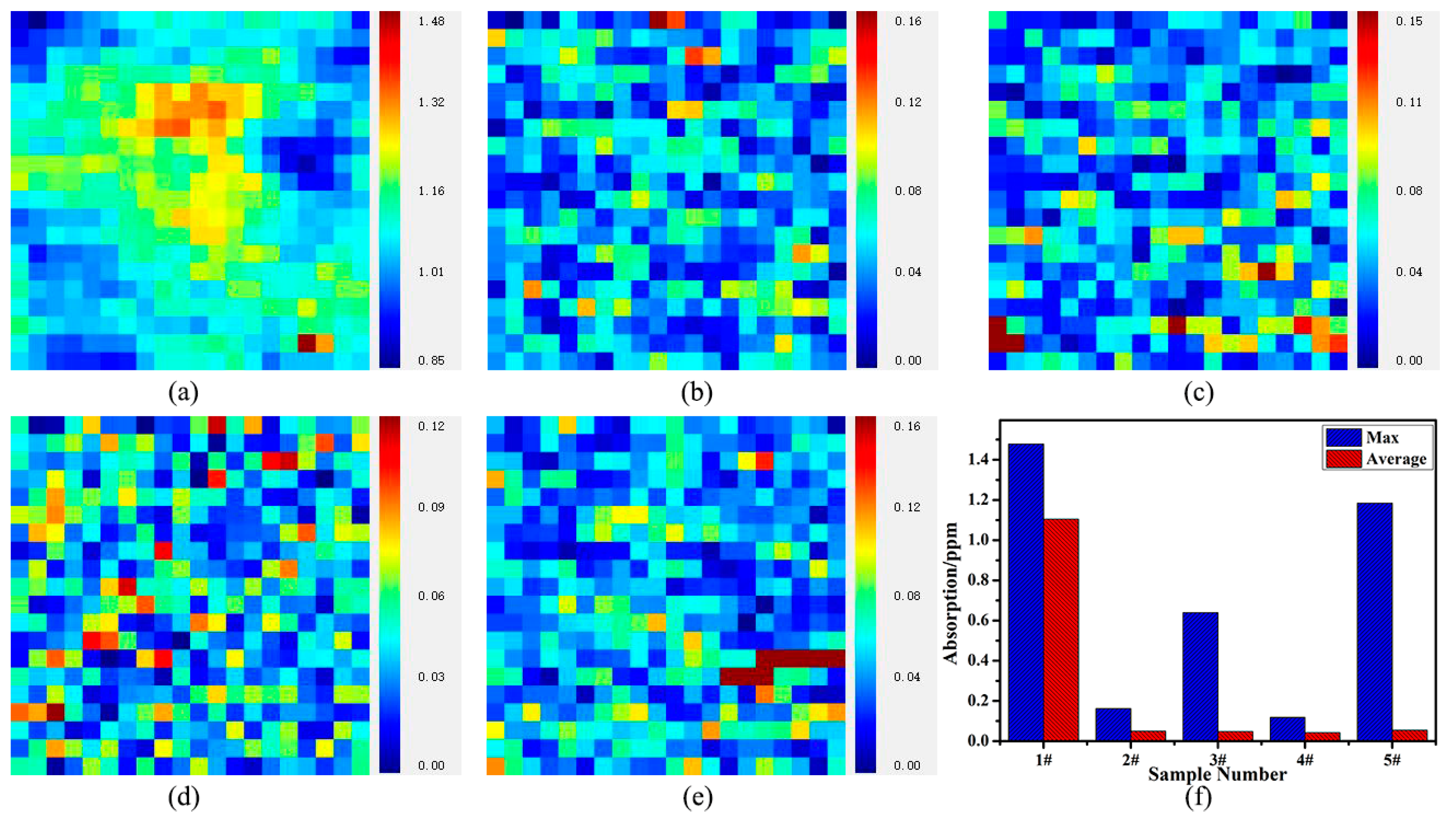
3.2. Photothermal Weak Absorption Analysis

To study the distribution of defects on the subsurface of quartz crystals, we performed UV absorption defect tests on samples with different etching depths. We used a large-diameter photothermal weak absorption test prototype to test the weak absorption of samples 1–5#. A 355 nm laser with a pump light of 1 mW was used as the excitation light, and the test area was 10 mm × 10 mm with a test step size of 500 microns. The test results are shown in Figure 3. The photothermal weak absorption characterization results show that after RIE etching, the average value of weak absorption of quartz crystals decreased greatly, indicating that RIE etching can effectively remove the subsurface defects of quartz crystals. Comparing the average weak absorption values in Figure 3f, we found that the surface defect layer of the quartz crystal was the main reason for the high weak absorption value, and when the surface defect layer was removed, the weak absorption value of the subsurface defect layer was relatively low. Additionally, comparing the maximum weak absorption values, we found that with the increase in the plasma etching time, the weak absorption values first decreased sharply, then increased, decreased again, and then increased again when etching at 5000 nm. The weak absorption value decreased rapidly when etching at 100 nm because the surface defect layer of the quartz crystal was removed at this time. When etching at 500 nm, the weakest value of absorption increased, mainly due to the fact that the etching process exposed the subsurface defects of the quartz crystal. Increasing the etching depth to 1000 nm resulted in a decrease in the average value of absorption to about the same as when etching at 100 nm, and the maximum value reached the minimum, indicating that the sub-surface defect layer was completely removed. However, when the etching depth was increased to 5000 nm, many sub-wavelength structures were generated in the sample due to the long RIE etching time, which modulated the light field and led to a sharp increase in the maximum value of weak absorption. The photothermal weak absorption test results coincide with the results of the white light test, and an appropriate RIE etching depth was able to effectively remove the defects of quartz crystals without introducing impurities.

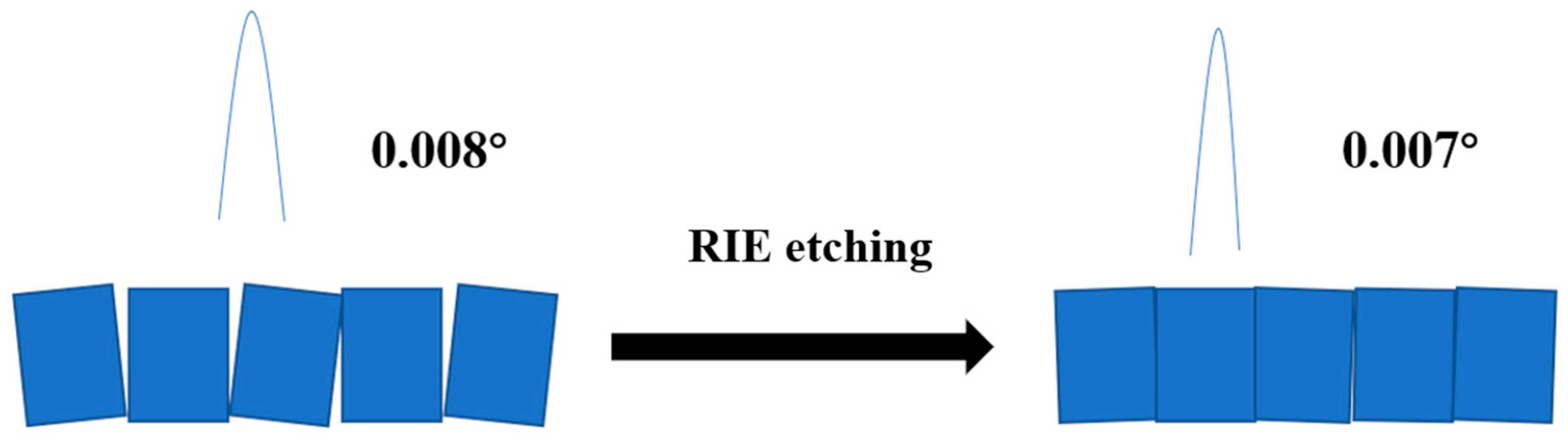
3.3. X-ray Diffraction Analysis

To investigate the relationship between the lattice of the crystals and the plasma etching time, we used an X-ray diffractometer to test the rocking curves of the crystalline surfaces of each sample 002. This instrument has a test limit half-height width of 3.5% and a test angle of incidence of about 16.56°. The diffraction intensity was related to the photon counts but not to the crystal structure. The half-height width of the rocking curve reflected the structural arrangement of the crystal lattice, and a smaller width indicated a neater orientation distribution of the lattice. The half-height widths of the rocking curves for each sample are shown in Figure 4. Additionally, we have included a schematic diagram of the changes in the lattice arrangement of quartz crystals after RIE treatment in Figure 5.
The full width at half maximum of the etched samples became smaller except for sample 3#, and the lattice arrangement of samples 2#, 4#, and 5# became more orderly after etching. However, the lattice arrangement of sample 3# was almost unchanged. Combining this test result with white light interference and photothermal weak absorption, we found that these three tests are consistent with each other. When the etching depth reached 500 nm, we observed that the values of roughness and weak absorption were larger than those of other etched samples. Surface lattice defects are an important factor that mainly affects the increase in roughness and weak absorption. For instance, when the crystal cells are too dispersed, the gaps inside the crystal are larger, which causes a large temperature difference inside the crystal when irradiated with laser light, resulting in higher weak absorption values. Moreover, the results of this study demonstrate that the lattice defects in quartz crystals are further corrected after RIE etching, which has an extremely important influence on the threshold value increase during the damage test. Generally, the damage occurs on the front surface of the crystal, and when the cell arrangement of the crystal sample is too dispersed, it increases the chance of damage and makes it easy to cause damage across the front and back surfaces during the damage process. Therefore, the RIE process is an important addition to the damage threshold enhancement of crystal samples.

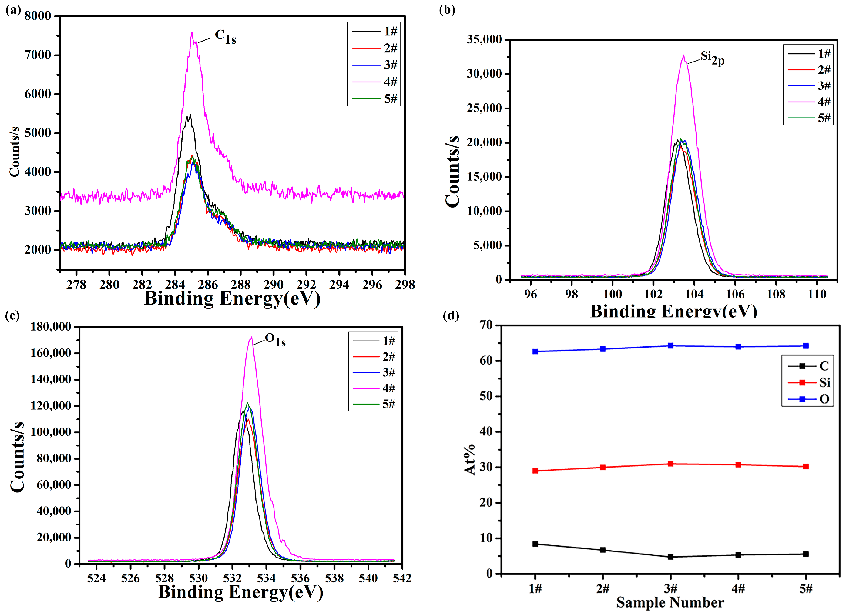
3.4. Chemical Structure Analysis

In order to study the elemental content and state of each sample surface before and after etching, we used XPS to characterize it, and the test elements were C, Si, and O. The test results are shown in Figure 6.
Prior to the XPS measurements, the top carbon contamination layer was cleaned using Ar ion beam sputtering for 100 s. Figure 6 illustrates the variation of Si, C, and O elements for samples with different etching depths. Firstly, we observed that the test peaks of sample 1# were higher than the other samples for all elements. This is mainly due to the fact that sample 1# was divided into two tests with the other samples during the test process, and the number of particles was different during these two tests, resulting in the peaks being too large. Secondly, the position of the peaks of each element for samples with different etching depths indicates that the peaks of each element were basically the same after etching. This suggests that no new elements were introduced during the etching process, demonstrating that the RIE etching process was able to remove the damage precursors from the samples effectively without introducing new elements. In addition, comparing Figure 6d, it can be noticed that the content of Si elements as well as O elements changed after etching. This is mainly due to the fact that RIE etching involves physical sputtering and a chemical reaction. During the etching process, CHF3 reacts with SiO2 to produce fluorine-based gases, which can cause changes in elemental content. At the same time, since the chemical reaction process of the sample indication does not react uniformly, it causes pits in the sample indication, so the sample should be modified by controlling the etching parameters to modulate the physical sputtering process during the etching process. The carbon content of the quartz crystal is significantly reduced, indicating that the etching process can effectively reduce the C contamination of the sample, thus improving the damage threshold of the quartz crystal.

3.5. Fluorescence Spectral Analysis

To better predict the damage threshold of each sample before the damage test, we conducted a fluorescence absorption test for samples with different etching depths, as shown in Figure 7. Since the sample is intended for use in the UV band, we compared the UV absorption of the samples. It was found that Sample #1 had the highest absorption, which is consistent with the high defect density. Sample #5 had the lowest absorption at multiple wavelengths, which is consistent with the removal of surface defects and with our characterization of the damage precursor. Moreover, the results of this study confirm that the RIE etching process can effectively remove the damage precursors of quartz crystals and enhance their damage threshold [30].

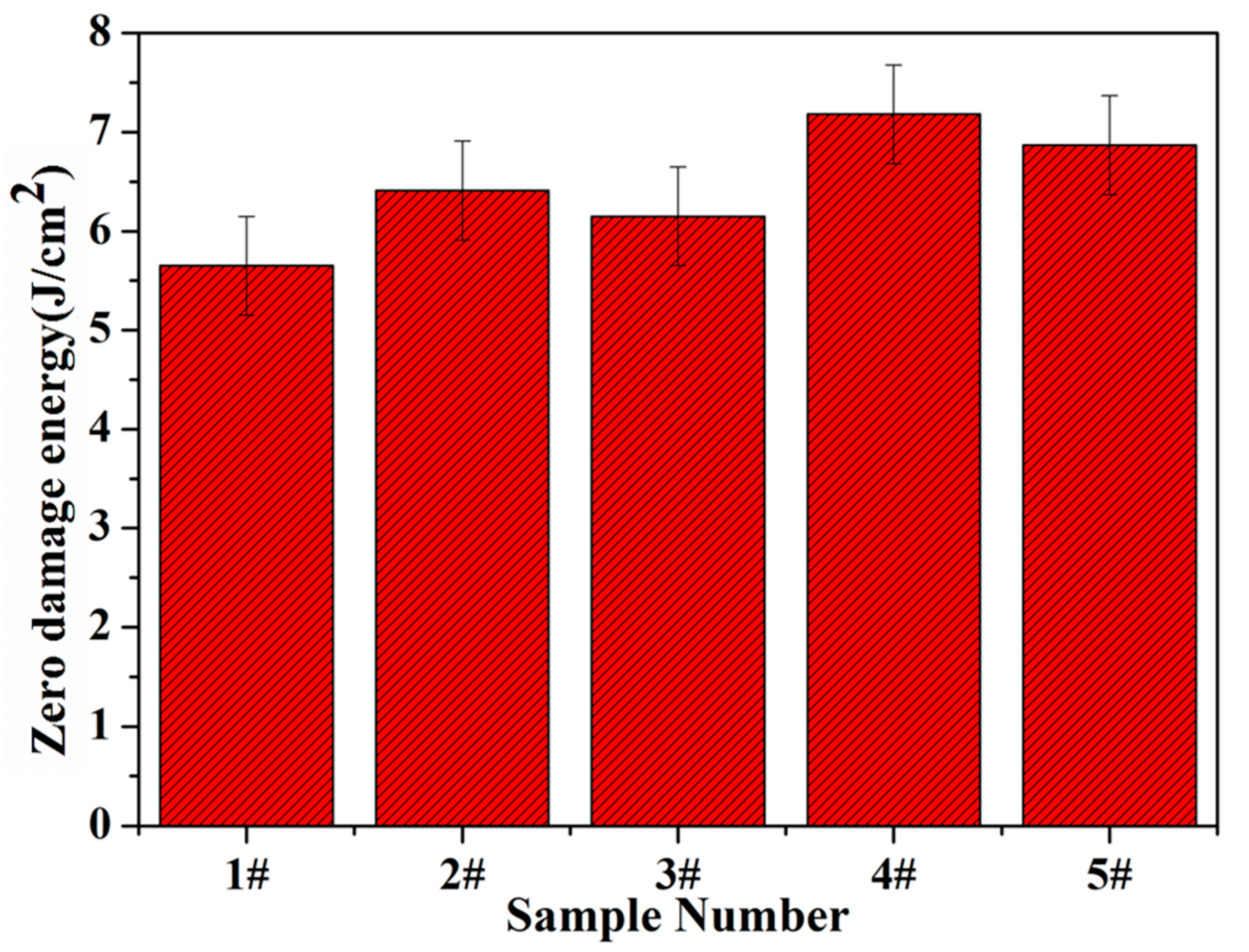
3.6. Laser Damage Threshold of the Sample

To better verify the enhancement effect of the RIE etching process on the damage performance of the samples and the consistency of the fluorescence absorption test results, we conducted damage tests on samples with different etching depths using a small-diameter UV laser damage test platform. Firstly, we took a random energy value for the damage threshold test according to the previous experience value. We tested 20 points under this energy to find out whether the optical components would be damaged and the probability of damage occurring in the sample. After determining the probability of damage at this energy density, we changed the output energy of the laser and took N gradient values for the damage test until it was stopped, and when damage occurred to the sample, the laser was applied. During the testing process, we ensured that the laser output parameters were consistent, and we used the R-on-1 method for the test, with each energy irradiated 20 times. Figure 8 shows the evolution of the zero damage probability of the RIE-etched element with the etching depth. From the figure, we observe that the damage test results coincide with the damage precursor detection results. The un-etched sample had the lowest zero-damage probability, and the damage threshold of the sample increased as the quartz crystal surface defects were removed. However, when the etching depth was increased to 500 nm, the threshold decreased due to the sub-surface defect layer, which also matches our test results. The sample had the highest zero-damage threshold when the etching depth was less than 1000 nm. The damage test results also demonstrate that the damage of UV quartz crystal components was mainly due to lattice defects, and the RIE etching process was able to correct the lattice of quartz crystals and remove surface and subsurface defects.

4. Conclusions

RIE etching is an effective method for removing damage precursors from the surface and subsurface of quartz crystals. Choosing the appropriate etching depth (1000 nm) can remove the damage precursors without causing secondary damage to the subsurface and interior of the optical element. The choice of plasma etching depth has a significant influence on the treatment of quartz crystal damage precursors. Selecting the appropriate plasma etching depth can modify the crystal cells within the crystal without causing damage to the subsurface and internal damage to the optical components. Additionally, appropriate plasma etching depth can completely remove the damage precursors on the surface of the element without increasing the surface roughness. Furthermore, plasma etching does not introduce secondary carbon contamination to the sample and can effectively improve the damage threshold of the optical element.

Author Contributions

Conceptualization, Q.L.; Methodology, Y.Z., Z.S., W.L. and X.Y.; Formal analysis, Q.L. and Y.Z.; Investigation, Q.L.; Data curation, Q.L. and Y.Z.; Writing—original draft, Q.L.; Writing—review & editing, Y.Z.; Supervision, Z.S., W.L. and X.Y.; Project administration, Z.S.; Funding acquisition, Q.L. and Z.S. All authors have read and agreed to the published version of the manuscript.

Funding

Joint Fund of the National Natural Science Foundation of China and the China Academy of Engineering Physics (Grant No. U1830203). The Open Project Program of Key Laboratory for Cross-Scale Micro and Nano Manufacturing, Ministry of Education, Changchun University of Science and Technology (CMNM-KF 202110).

Data Availability Statement

The data presented in this study are available upon request from the corresponding author. The data are not publicly available as related work is still being submitted for publication.

Conflicts of Interest

The authors declare no conflict of interest.

References

  1. Feng, Q.; Deng, H.; Huang, S.; Li, B.; Xiang, X.; Li, L.; Zu, X. Strong UV laser absorption source near 355 nm in fused silica and its origination. Opt. Express 2021, 29, 31849–31858. [Google Scholar] [CrossRef]
  2. Xiao, P.; Xin, C.; Chao, W.; Song, W.; Kai, N.; Zhen, N.; Yi, H.; Zhi, J.; Zhen, C.; Jian, S. Laser-based defect characterization and removal process for manufacturing fused silica optic with high ultraviolet laser damage threshold. Light Adv. Manuf. 2023, 4, 21. [Google Scholar]
  3. Zhong, Y.; Dai, Y.; Shi, F.; Song, C.; Tian, Y.; Lin, Z.; Shen, Y. Effects of ion beam etching on the nanoscale damage precursor evolution of fused silica. Materials 2020, 13, 1294. [Google Scholar] [CrossRef]
  4. Suratwala, T.I.; Miller, P.E.; Bude, J.D.; Steele, W.A.; Shen, N.; Monticelli, M.V.; Wong, L.L. HF-based etching processes for improving laser damage resistance of fused silica optical surfaces. J. Am. Ceram. Soc. 2011, 94, 416–428. [Google Scholar] [CrossRef]
  5. Zhang, Y.; Song, C.; Shi, F.; Tian, Y.; Lin, Z. Research on rapid repairing of surface laser damage of fused silica optics. In Second Target Recognition and Artificial Intelligence Summit Forum; SPIE: Bellingham, WA, USA, 2020; Volume 11427, pp. 1006–1012. [Google Scholar]
  6. Long, J.; Ross, D.; Tastepe, E.; Lamb, M.; Funamoto, Y.; Shima, D.; Yamaguchi, H. Fused silica contamination layer removal using magnetic field-assisted finishing. J. Am. Ceram. Soc. 2020, 103, 3008–3019. [Google Scholar] [CrossRef]
  7. Li, Y.; Yuan, Z.; Wang, J.; Xu, Q. Laser-induced damage characteristics in fused silica surface due to mechanical and chemical defects during manufacturing processes. Opt. Laser Technol. 2017, 91, 149–158. [Google Scholar] [CrossRef]
  8. Menapace, J.A.; Penetrante, B.; Miller, P.E.; Parham, T.; Nichols, M.; Peterson, J.; Slomba, A. Combined advanced finishing and UV-laser conditioning for producing UV-damage-resistant fused silica optics. In Optical Fabrication and Testing; Optica Publishing Group: Washington, DC, USA, 2002; p. OMB4. [Google Scholar]
  9. Ishizuki, H.; Yahia, V.; Taira, T. Characteristics of crystal quartz for high-intensity, sub-nanosecond wavelength conversion. Opt. Mater. Express 2018, 8, 1259–1264. [Google Scholar] [CrossRef]
  10. Guo, X.; Yuan, S.; Huang, J.; Chen, C.; Kang, R.; Jin, Z.; Guo, D. Effects of pressure and slurry on removal mechanism during the chemical mechanical polishing of quartz glass using ReaxFF MD. Appl. Surf. Sci. 2020, 505, 144610. [Google Scholar] [CrossRef]
  11. Zhao, Z.; Zhang, Z.; Shi, C.; Feng, J.; Zhuang, X.; Li, L.; Liu, D. Dispersion and polishing mechanism of a novel CeO2-LaOF-Based chemical mechanical polishing slurry for quartz glass. Materials 2023, 16, 1148. [Google Scholar] [CrossRef]
  12. Lapitskaya, V.A.; Kuznetsova, T.A.; Khudoley, A.L.; Khabarava, A.V.; Chizhik, S.A.; Aizikovich, S.M.; Sadyrin, E.V. Influence of polishing technique on crack resistance of quartz plates. Int. J. Fract. 2021, 231, 61–77. [Google Scholar] [CrossRef]
  13. Wang, Z.; Yan, H.; Yuan, X.; Li, Y.; Yang, K.; Yan, L.; Li, H. The effect of dynamic etching on surface quality and laser damage resistance for fused silica optics. In Fourth International Symposium on Laser Interaction with Matter; SPIE: Bellingham, WA, USA, 2017; Volume 10173, pp. 502–508. [Google Scholar]
  14. Shi, F.; Zhong, Y.; Dai, Y.; Peng, X.; Xu, M.; Sui, T. Investigation of surface damage precursor evolutions and laser-induced damage threshold improvement mechanism during Ion beam etching of fused silica. Opt. Express 2016, 24, 20842–20854. [Google Scholar] [CrossRef]
  15. Sun, L.; Shao, T.; Zhou, X.; Li, W.; Li, F.; Ye, X.; Zheng, W. Understanding the effect of HF-based wet shallow etching on optical performance of reactive-ion-etched fused silica optics. RSC Adv. 2021, 11, 29323–29332. [Google Scholar] [CrossRef]
  16. Hu, X.; Ye, X.; Wu, J.; Chen, S.; Chen, Y.; Huang, J.; Zheng, W. Effect of radio frequency power on nano-metal induced self-masking subwavelength structures mechanism. Results Phys. 2020, 16, 103155. [Google Scholar] [CrossRef]
  17. Sun, Y.; Hu, X.; Zhang, H.; Lai, F.; Zheng, Y.; Yan, L.; Zhang, X. SiO2–ORMOSIL double-layered broadband antireflective coating for high-power laser system. J. Sol-Gel Sci. Technol. 2016, 79, 558–563. [Google Scholar] [CrossRef]
  18. Ye, X.; Shao, T.; Sun, L.; Wu, J.; Wang, F.; He, J.; Zheng, W. Plasma-induced, self-masking, one-step approach to an ultrabroadband antireflective and superhydrophilic subwavelength nanostructured fused silica surface. ACS Appl. Mater. Interfaces 2018, 10, 13851–13859. [Google Scholar] [CrossRef]
  19. Sun, L.; Ni, R.; Xia, H.; Shao, T.; Huang, J.; Ye, X.; Cao, L. Theoretical and experimental research on laser-induced damage of fused silica optics due to stimulated Brillouin scattering. IEEE Photonics J. 2018, 10, 1–15. [Google Scholar] [CrossRef]
  20. Merkle, L.D.; Bass, M.; Swimm, R.T. Multiple Pulse Laser-Induced Bulk Damage in Crystalline and Fused Quartz at 1.064 and 0.532 õm. Opt. Eng. 1983, 22, 405–410. [Google Scholar] [CrossRef]
  21. Liu, T.; Yang, K.; Zhang, Z.; Yan, L.; Huang, B.; Li, H.; Yan, H. Hydrofluoric acid–based etching effect on surface pit, crack, and scratch and laser damage site of fused silica optics. Opt. Express 2019, 27, 10705–10728. [Google Scholar] [CrossRef]
  22. Cao, Z.; Wei, C.; Cheng, X.; Zhao, Y.; Peng, X.; Jiang, Z.; Shao, J. Ground fused silica processed by combined chemical etching and CO2 laser polishing with super-smooth surface and high damage resistance. Opt. Lett. 2020, 45, 6014–6017. [Google Scholar] [CrossRef]
  23. Chai, X.; Li, P.; Zhao, J.; Wang, G.; Zhu, D.; Jiang, Y.; Jing, Y. Laser-induced damage growth of large-aperture fused silica optics under high-fluence 351 nm laser irradiation. Optik 2021, 226, 165549. [Google Scholar] [CrossRef]
  24. Zhong, Y.; Dai, Y.; Tian, Y.; Shi, F. Effect on nanoscale damage precursors of fused silica with wet etching in KOH solutions. Opt. Mater. Express 2021, 11, 884–894. [Google Scholar] [CrossRef]
  25. Li, B.; Sun, W.; Xiang, X.; Jiang, X.; Liao, W.; Wang, H.; Zu, X. A two-step physical-chemical etching technique to improve laser damage resistance of fused silica. J. Mater. Res. Technol. 2022, 19, 3231–3240. [Google Scholar] [CrossRef]
  26. Yang, D.; Cheng, J.; Zhao, L.; Chen, M.; Liu, H.; Wang, J.; Xu, Q. Evolution of the point defects involved under the action of mechanical forces on mechanically machined fused silica surfaces. Opt. Express 2023, 31, 7684–7706. [Google Scholar] [CrossRef] [PubMed]
  27. Ma, Y.; Zheng, Q.; Wang, F.; Sun, L.; Yu, J.; He, H. Evolution of physical and mechanical properties of fused silica after subsurface damage layer removal by RIE treatment. J. Non-Cryst. Solids 2023, 616, 122475. [Google Scholar] [CrossRef]
  28. Miller, P.E.; Suratwala, T.I.; Wong, L.L.; Feit, M.D.; Menapace, J.A.; Davis, P.J.; Steele, R.A. The distribution of subsurface damage in fused silica. In Laser-Induced Damage in Optical Materials: 2005; SPIE: Bellingham, WA, USA, 2006; Volume 5991, p. 599101. [Google Scholar]
  29. Sun, R.; Huang, Y.; Zhang, X.; Zhao, F.; Zhang, Y.; Liu, J.; Hu, J. Study on subsurface damage of fused quartz in grinding stage. In Eighth Symposium on Novel Photoelectronic Detection Technology and Applications; SPIE: Bellingham, WA, USA, 2022; Volume 12169, p. 1216902. [Google Scholar]
  30. Xu, M.; Shi, F.; Zhou, L.; Dai, Y.; Peng, X.; Liao, W. Investigation of laser-induced damage threshold improvement mechanism during ion beam sputtering of fused silica. Opt. Express 2017, 25, 29260–29271. [Google Scholar] [CrossRef]
Figure 1. Schematic diagram of RIE etching principle.
Crystals 13 01477 g001
Figure 2. Schematic representation of the surface roughness of the samples with different etching depths. (ae) Surface morphology of sample #1 to sample #5, respectively. (f) Roughness statistics of samples with different etching depths.
Crystals 13 01477 g002
Figure 3. Weak absorption statistics for samples with different etching depths. (ae) Distribution of photothermally weak absorption of samples from sample #1 to sample #5, respectively. (f) Statistics of the average and maximum values of photothermally weak absorption of samples with different etching depths.
Crystals 13 01477 g003
Figure 4. Half-height width of the rocking curve for each sample.
Crystals 13 01477 g004
Figure 5. Schematic diagram of changes in lattice arrangement of quartz crystals after RIE etching.
Crystals 13 01477 g005
Figure 6. XPS schematic diagrams of samples with different etching depths. Schematic diagrams of the test peaks for the element C1s are given in (a), the test peaks for the element Si2p are given in (b), the test peaks for the element O1s are given in (c), and the statistical curves of the distribution of the content of each element in different samples are given in (d).
Crystals 13 01477 g006
Figure 7. Schematic diagram of fluorescence absorption of different etched samples.
Crystals 13 01477 g007
Figure 8. Statistical plot of zero damage threshold for samples with different etching processes.
Crystals 13 01477 g008
Table 1. Quartz crystal processing technology table.
Sample Number1#2#3#4#5#
Etching depth (nm)010050010005000
Disclaimer/Publisher’s Note: The statements, opinions and data contained in all publications are solely those of the individual author(s) and contributor(s) and not of MDPI and/or the editor(s). MDPI and/or the editor(s) disclaim responsibility for any injury to people or property resulting from any ideas, methods, instructions or products referred to in the content.

