
Characterization of Defects in GaN: Optical and Magnetic Resonance Techniques


Abstract
1. Introduction
2. Experimental Methods
2.1. Technical Approach
2.2. Samples
3. Experimental Results and Discussion
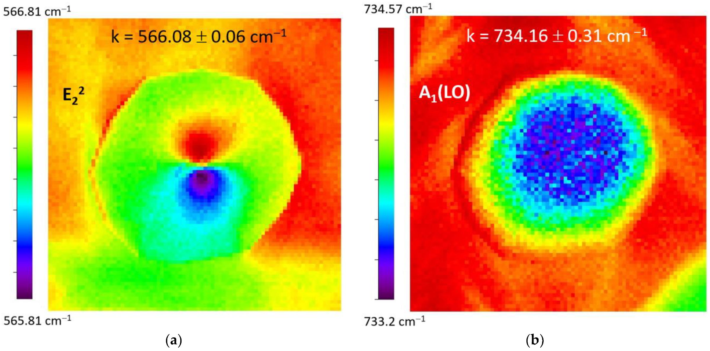
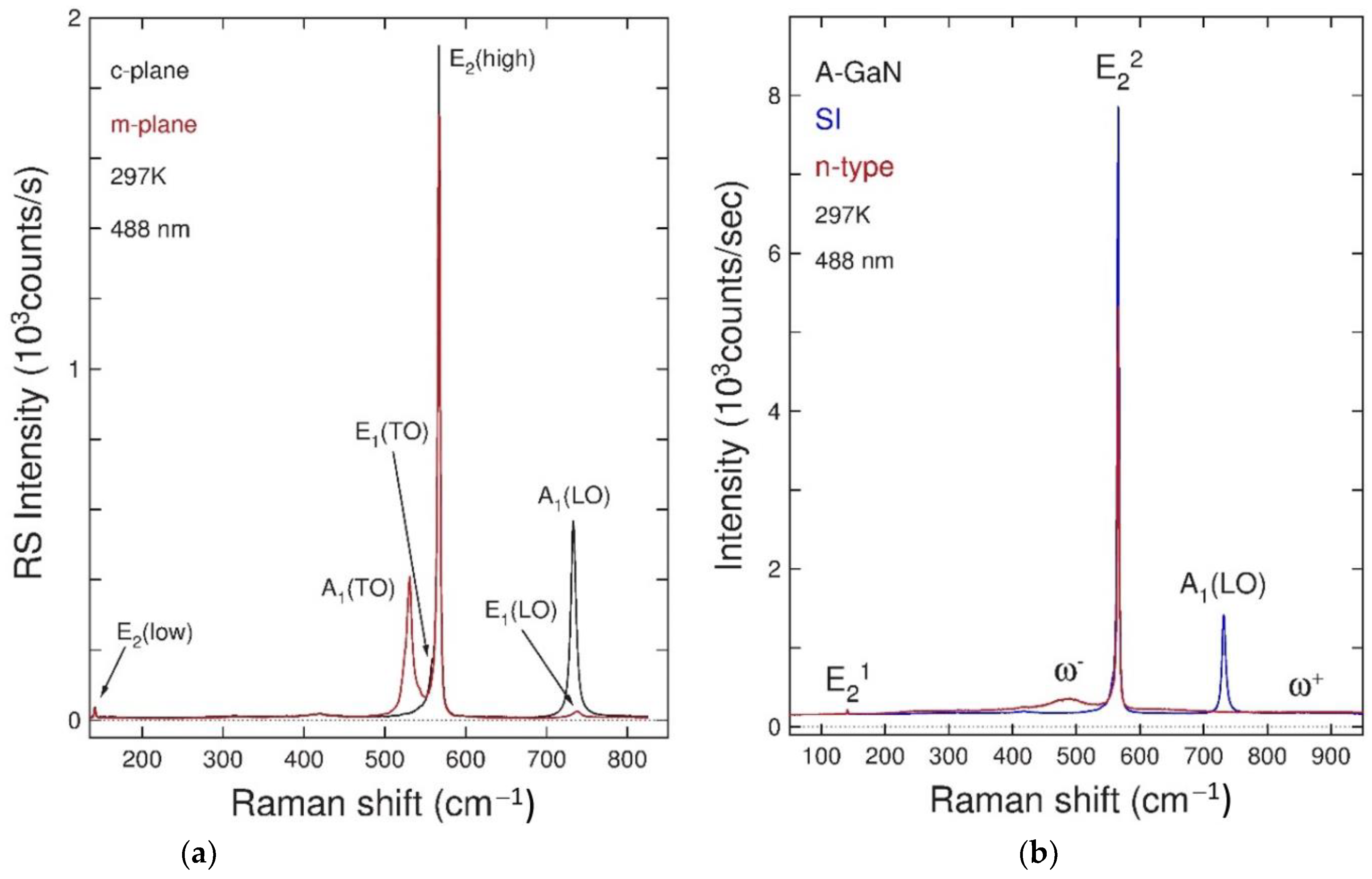
3.1. Raman Spectroscopy
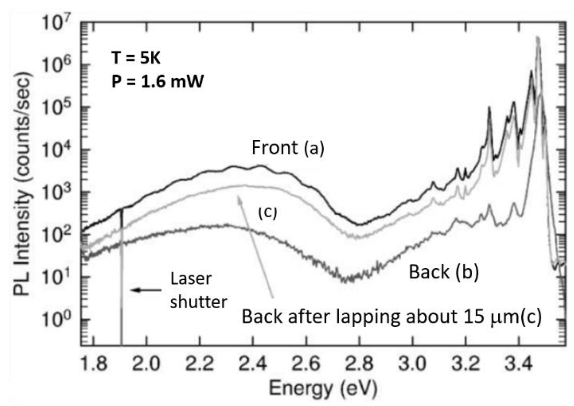
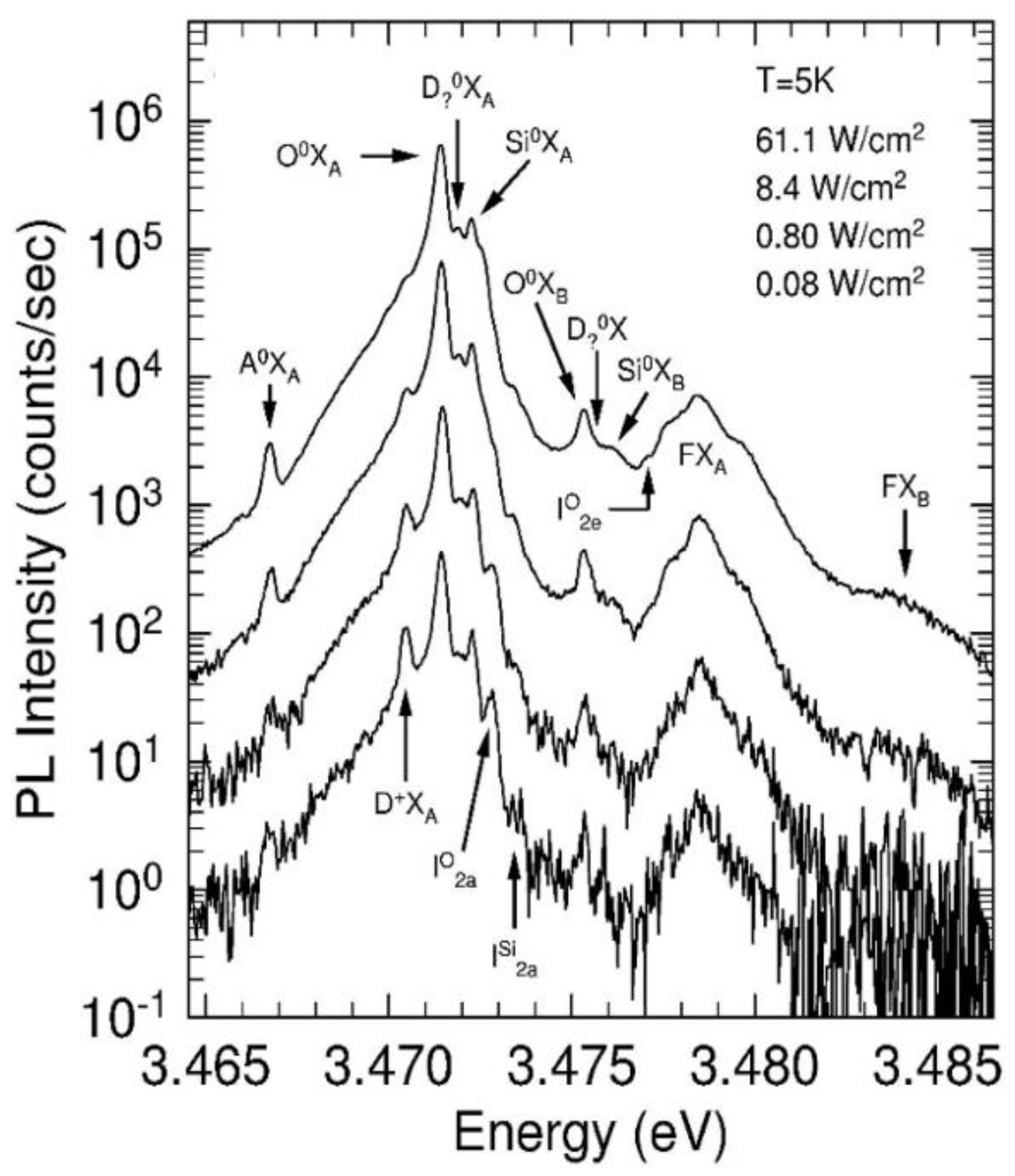
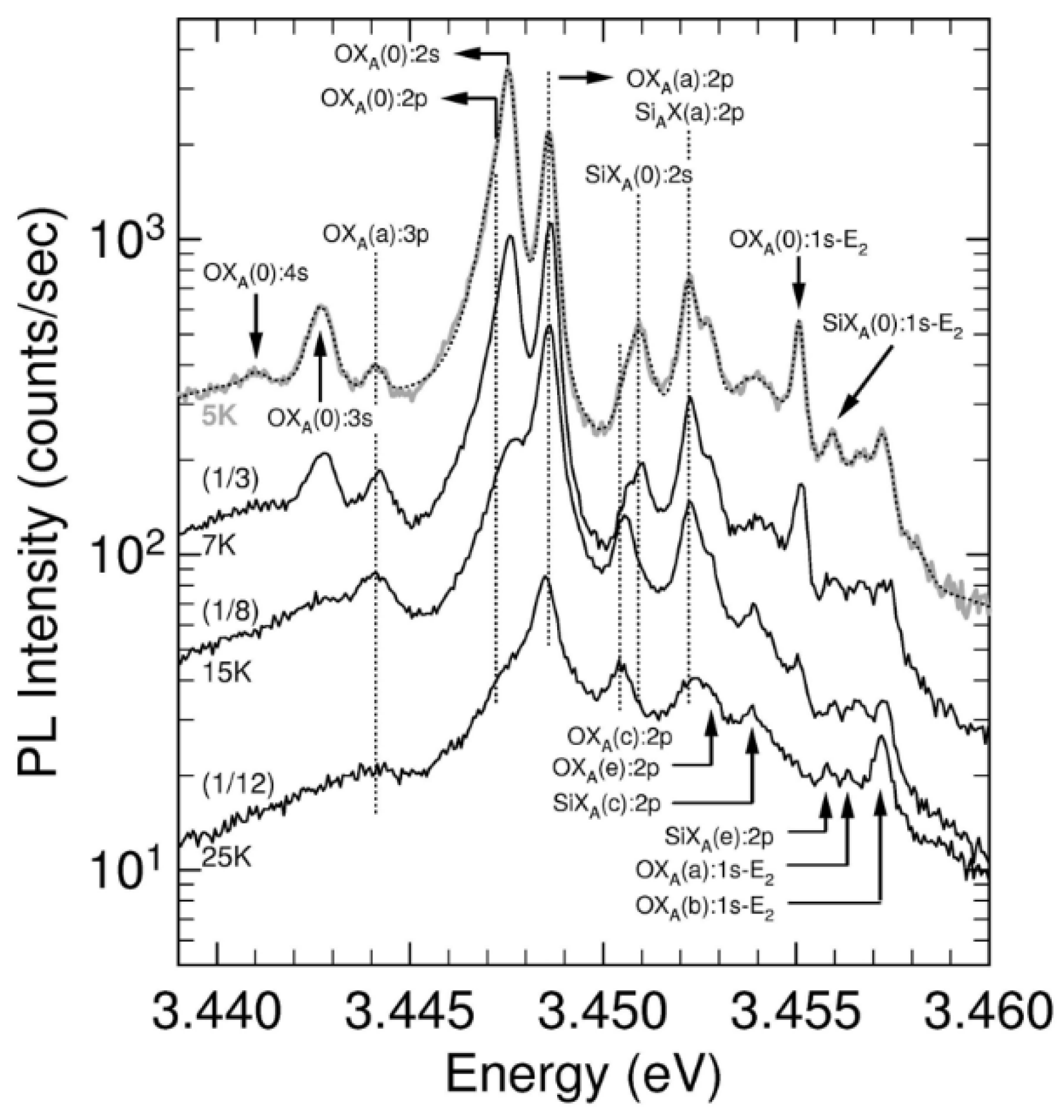
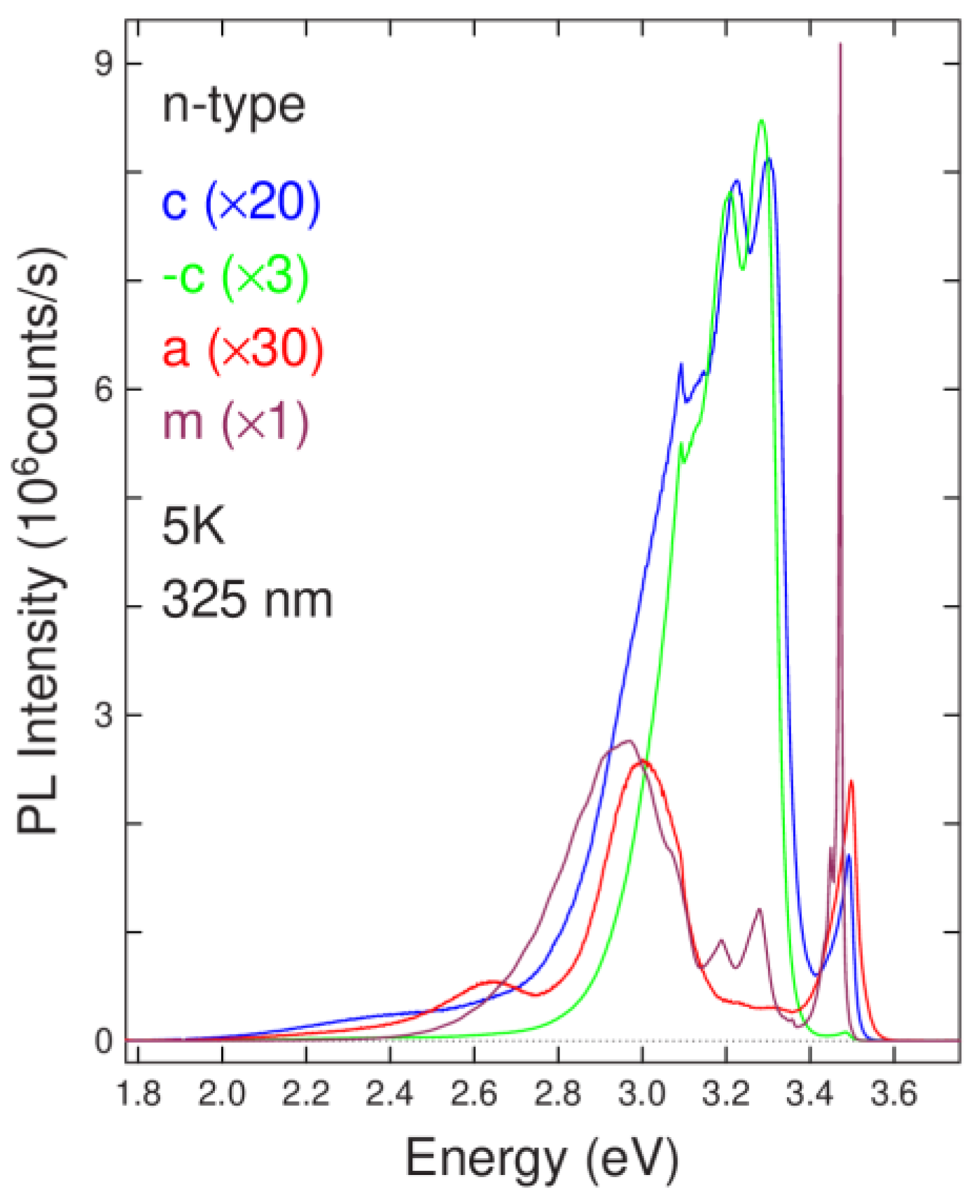
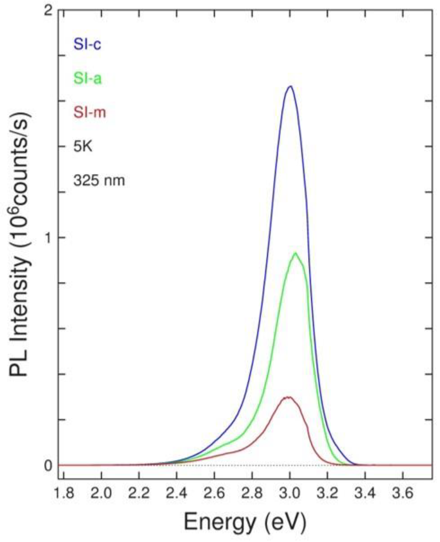
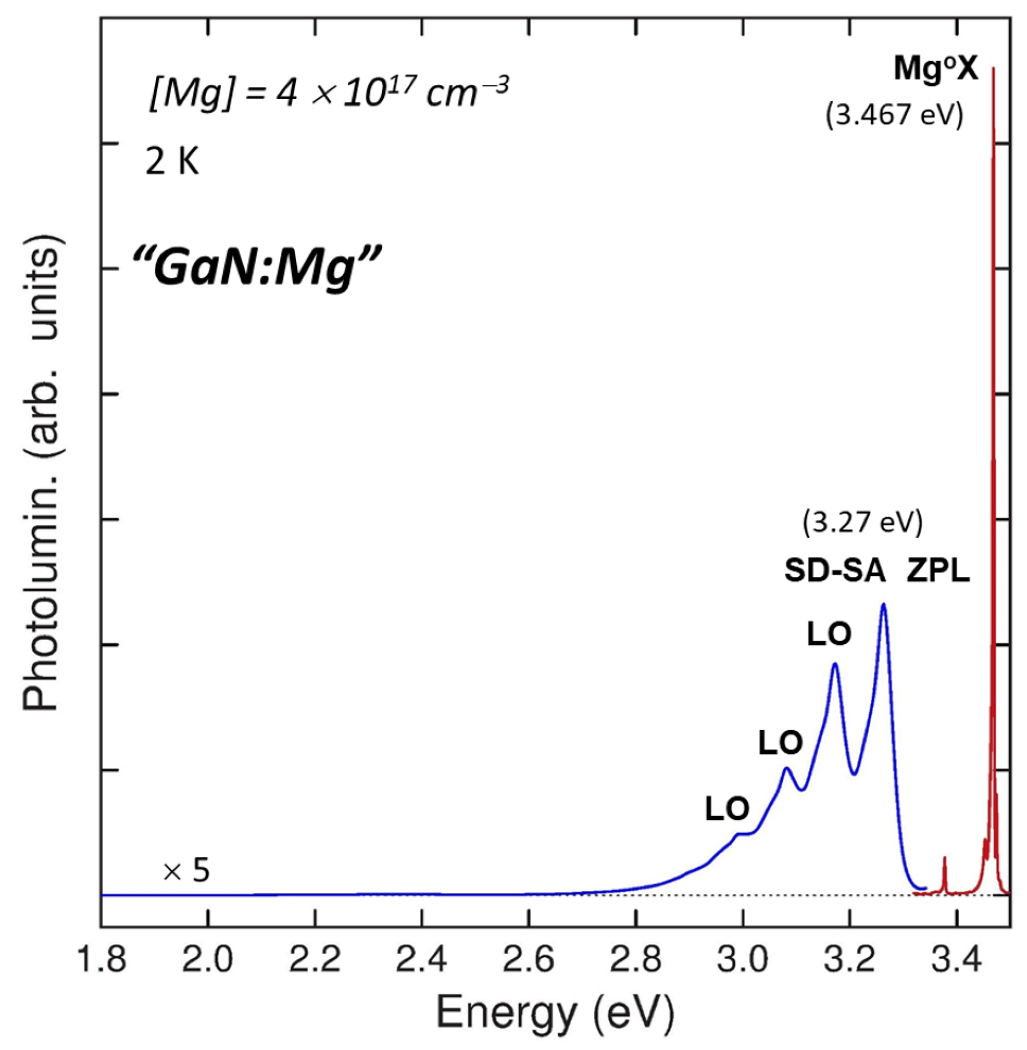
3.2. PL
3.3. Magnetic Resonance
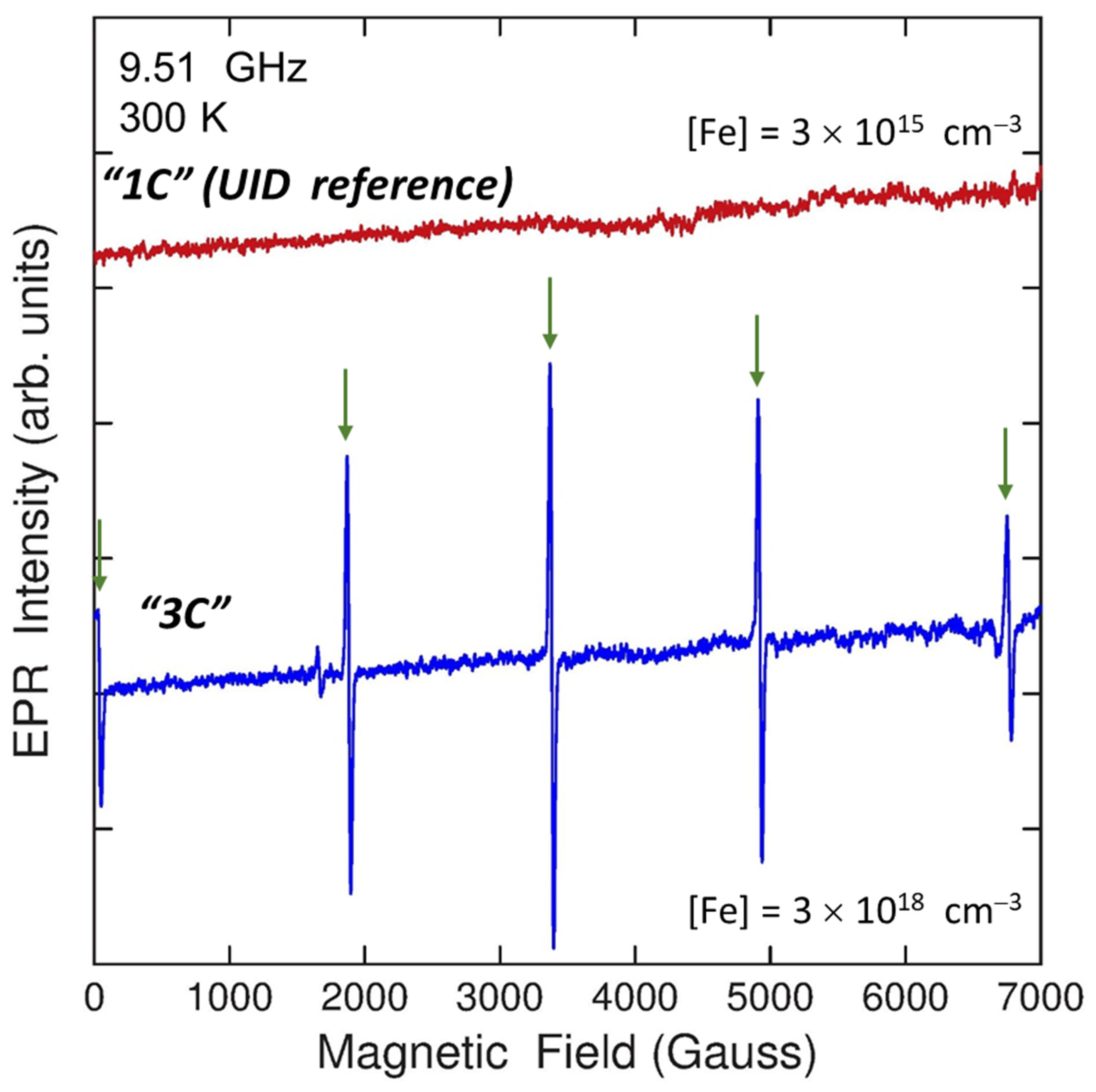
3.3.1. EPR
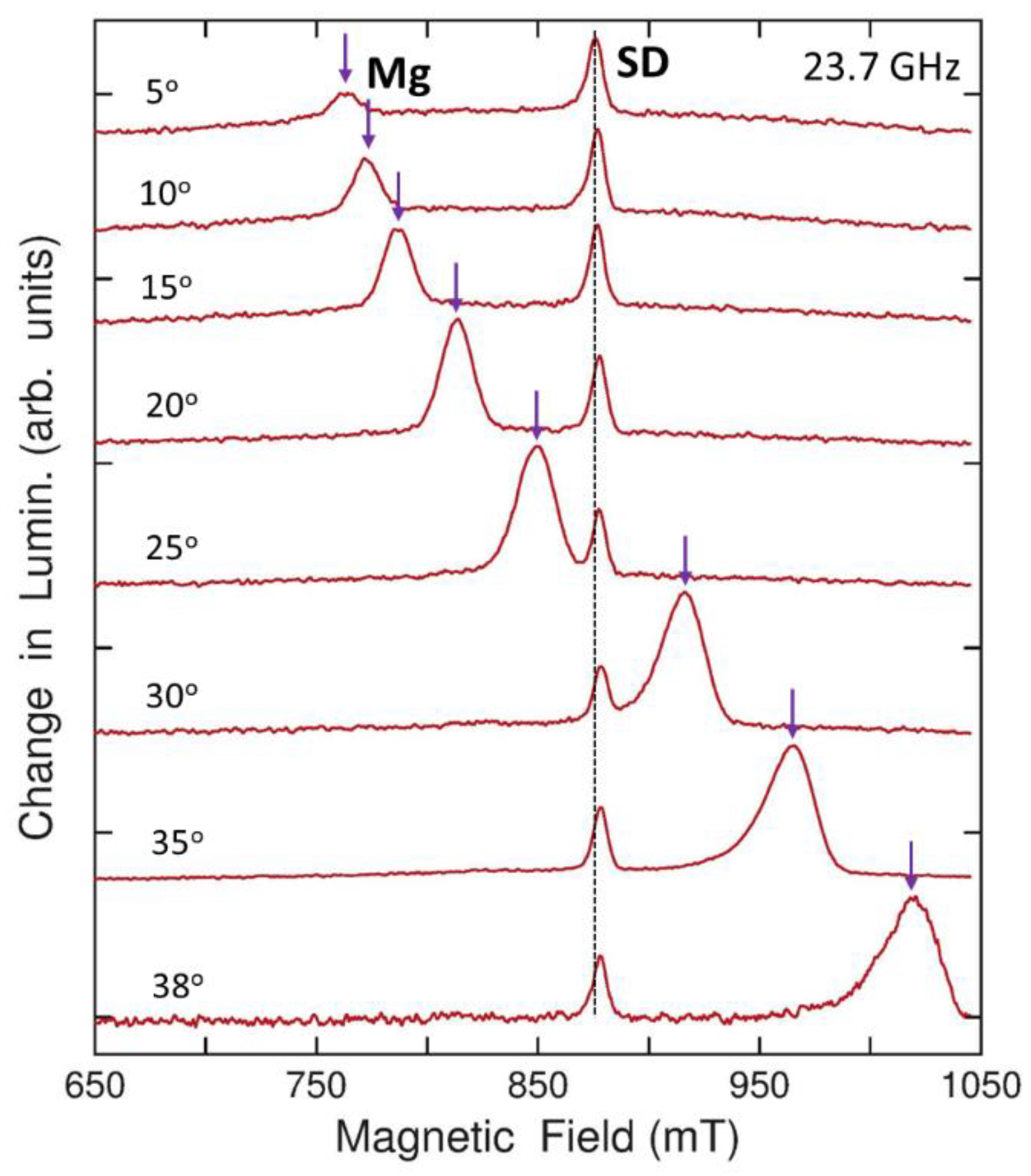
3.3.2. ODMR
4. Summary
Funding
Data Availability Statement
Conflicts of Interest
References
- Feigelson, B.N.; Frazier, R.M.; Freitas, J.A., Jr.; Fatemi, M.; Mastro, M.A.; Tischler, J.G. Seeded growth of GaN single crystals from solution at near atmospheric pressure. J. Cryst. Growth 2008, 310, 3934–3940. [Google Scholar] [CrossRef]
- Yamane, H.; Shimada, M.; DiSalvo, F.J. Na flux growth and characterization of GaN single crystals. Mater. Sci. Forum 2000, 325, 21–24. [Google Scholar] [CrossRef]
- Grezegory, I.; Bockowski, M.; Luznik, B.; Krukowski, K.; Romanowski, Z.; Wroblewski, M.; Porowski, S. Mechanism of crystallization of bulk GaN from solution under high N3 pressure. J. Cryst. Growth 2002, 246, 177–186. [Google Scholar] [CrossRef]
- Porowski, S.; Sadovyi, B.; Karbovnyk, I.; Gierlotka, S.; Rzoska, S.J.; Petrusha, I.; Stratiichuk, D.; Turkevich, V.; Grzegory, I. Melting of tetrahedrally bonded semiconductors: “anomaly” of the phase diagram of GaN. J. Cryst. Growth 2019, 505, 5–9. [Google Scholar] [CrossRef]
- Yoshida, S.; Misawa, S.; Gonda, S. Improvements on the electrical and luminescent properties of reactive molecular beam epitaxially grown GaN films by using AlN-coated sapphire substrates. Appl. Phys. Lett. 1983, 42, 427. [Google Scholar] [CrossRef]
- Amano, H.; Sawaki, N.; Akasaki, I.; Toyoda, T. Metalorganic vapor phase epitaxial growth of a high quality GaN film using an AlN buffer layer. Appl. Phys. Lett. 1986, 48, 353. [Google Scholar] [CrossRef]
- Nakamura, S. Thermal Annealing Effects on P-Type Mg-Doped GaN Films. Jpn. J. Appl. Phys. 1992, 31, L139. [Google Scholar] [CrossRef]
- Kamiyama, S.; Amano, H.; Akasaki, I. The Evolution of Nitrides Semiconductors. In Optoeletronics Devices: III-Nitrides; Razighi, M., Henini, M., Eds.; Elsevier Ltd.: Amsterdam, The Netherlands, 2004; pp. 23–38. [Google Scholar]
- Bergman, L.; Dutta, M.; Nemanich, R.J. Raman Scattering in Materials Science; Springer Series in Material Science; Weber, W.H., Merlin, R., Eds.; Springer: Berlin/Heidelberg, Germany, 2000; Volume 42, p. 273. [Google Scholar]
- Maruska, H.P.; Tietjen, J.J. The preparation and properties of vapor-deposited single-crystal-line GaN. Appl. Phys. Lett. 1969, 15, 327. [Google Scholar] [CrossRef]
- Kelly, M.K.; Vaudo, R.P.; Phance, V.M.; Gögens, L.; Ambacher, O.; Stutzmanm, M. Large Free-Standing GaN Substrates by Hydride Vapor Phase Epitaxy and Laser-Induced Liftoff. Jpn. J. Appl. Phys. 1999, 38, L217. [Google Scholar] [CrossRef]
- Park, S.S.; Park, I.-W.; Choh, S.H. Free-Standing GaN Substrates by Hydride Vapor Phase Epitaxy. Jpn. J. Appl. Phys. 2000, 39, L1141–L1142. [Google Scholar] [CrossRef]
- Paskova, T.; Darakchieva, V.; Paskov, P.P.; Söderwall, U.; Monemar, B. Growth and separation related properties of HVPE-GaN free-standing films. J. Cryst. Growth 2002, 246, 207. [Google Scholar] [CrossRef]
- Yoshida, T.; Oshima, Y.; Eri, T.; Ikeda, K.; Yamamoto, S.; Watanabe, K.; Shibata, M.; Mishima, T.J. Fabrication of 3-in GaN substrates by hydride vapor phase epitaxy using void-assisted separation method. J. Cryst. Growth 2008, 310, 5–7. [Google Scholar] [CrossRef]
- Hanser, D.; Tudor, M.; Preble, E.A.; Williams, M.; Xu, X.; Tsvetkov, D.; Liu, L. Surface preparation of substrates from bulk GaN crystals. J. Cryst. Growth 2007, 305, 372. [Google Scholar] [CrossRef]
- Freitas, J.A., Jr.; Gowda, M.; Tischler, J.G.; Kim, J.-H.; Liu, L.; Hanser, D. Semi-insulating GaN substrates for high-frequency device fabrication. J. Cryst. Growth 2008, 310, 3968. [Google Scholar] [CrossRef]
- Ballman, A.A.; Dodd, D.M.; Kuebler, N.A.; Laudise, R.A.; Wood, D.L.; Rudd, D.W. Synthetic quartz with high ultraviolet transmission. Appl. Opt. 1968, 7, 1387. [Google Scholar] [CrossRef]
- Ehrentrautt, D.; Bockowski, M. Bulk crystal growth: Basic techniques, and growth mechanisms and dynamics. In Handbook of Crystal Growth, 2nd ed.; Rudoph, P., Ed.; Elsevier: Amsterdam, The Netherlands, 2015; pp. 577–619. [Google Scholar]
- Doradzinski, R.; Dwillinski, R.; Garcznski, J.; Sierzputowski, L.P.; Kanbara, Y. Technology of Galliun Nitride Crystal Growth; Ehrentraut, D., Meissiner, E., Bockowski, M., Eds.; Spring-Verlag: Berlin/Heidelberg, Germany, 2010; pp. 137–158. [Google Scholar]
- Wang, B.; Callahan, M.J. Ammonothermal Synthesis of III-Nitride Crystals. Cryst. Des. 2006, 6, 1227. [Google Scholar] [CrossRef]
- Dwillinski, R.; Doradzinski, R.; Garcznski, J.; Sierzputowski, L.P.; Kucharski, R.; Rudzinski, M.; Zajac, M.; Kudrawiec, R. Properties of truly bulk GaN monocrystals grown by ammonothermal method. Phys. Status Solid C 2009, 6, 2661. [Google Scholar] [CrossRef]
- Sochacki, T.; Amilusiki, M.; Lucznik, B.; Fijalkowski, M.; Weyhar, J.L.; Sadovyi, B.; Kamler, G.; Nowak, G.; Litwin-Staszewska, E.; Khachapuridze, A.; et al. Preparation of free-standing GaN substrates from GaN layers crystallized by hydride vapor phase epitaxy on ammonothermal GaN seeds. Jpn. J. Appl. Phys. 2014, 53, 05FA04. [Google Scholar] [CrossRef]
- Freitas, J.A., Jr.; Culbertson, J.C.; Mahadik, N.A.; Sochacki, T.; Bockowski, M.; Iwinska, M. Growth of high crystalline quality HVPE-GaN crystals with controlled electrical properties. Cryst. Growth Des. 2015, 15, 4837. [Google Scholar] [CrossRef]
- Kozawa, T.; Kachi, T.; Kano, H.; Nagase, H.; Koide, N.; Manabe, K. Thermal stress in GaN epitaxial layers grown on sapphire substrates. J. Appl. Phys. 1995, 77, 4389. [Google Scholar] [CrossRef]
- Freitas, J.A., Jr.; Culbertson, J.C.; Mahadik, N.A.; Glaser, E.R.; Sochccki, T.; Bockowski, M. Incorporation of pervasive impurities on HVPOE GaN growth directions. J. Cryst. Growth 2016, 456, 101–107. [Google Scholar] [CrossRef]
- Gogova, D.; Petrov, P.P.; Buegler, M.; Wagner, M.R.; Nestiel, C.; Callsen, G.; Schmidbauert, M.; Kucharski, R.; Zajac, M.; Dwilinski, R.; et al. Structural and optical investigation of non-polar (1–100) GaN grown by the ammonothermal method. J. Appl. Phys. 2013, 113, 203513. [Google Scholar] [CrossRef]
- Perlin, P.; Camassel, J.; Knap, W.; Talercio, T.; Chervin, J.C.; Suski, T.; Grzegory, I.; Porowski, S. Investigation of longitudinal-optical phonon-plasmon coupled modes in highly conducting bulk GaN. Appl. Phys. Lett. 1995, 67, 2524. [Google Scholar] [CrossRef]
- Kim, H.-Y.; Freitas, J.A., Jr.; Kim, J. Penetration Effects of High-Energy Protons in GaN: A Micro-Raman Spectroscopy Study. Electrochem. Sol.-St. Lett. 2011, 14, H5–H8. [Google Scholar] [CrossRef]
- Freitas, J.A., Jr.; Zajac, M. Chapter 16, Properties of Ammonthermal Crystals. In Ammonothermal Synthesis and Crystal Growth of Nitrides; Spring Series in Materials Science; Maissener, E., Niewa, R., Eds.; Springer: Cham, Switzerland, 2021; Volume 304, pp. 287–314. [Google Scholar]
- Zając, M.; Kucharski, R.; Grabianska, K.; Gwardys-Bak, A.; Puchalski, A.; Domagala, J.Z.; Piotrzkowski, R.; Litwin-Staszewska, E.; Wasik, D.; Bockowski, M. Basic ammonothermal growth of Gallium Nitride—State of the art, challenges, perspectives. Prog. Cryst. Growth Charact. Mat. 2018, 64, 63. [Google Scholar] [CrossRef]
- Freitas, J.A., Jr.; Culbertson, J.C.; Mahadik, N.A.; Sochacki, T.; Bockowski, M. HVPE GaN wafers with improved crystalline and electrical properties. J. Cryst. Growth 2016, 456, 113. [Google Scholar] [CrossRef]
- Freitas, J.A., Jr.; Khan, M.A. Raman and Photoluminescence Studies of Undoped and Magnesium-Doped Gan Films on Sapphire. Mat. Res. Soc. 1994, 339, 547. [Google Scholar] [CrossRef]
- Ogino, T.; Aoki, M. Mechanism of yellow luminescence in GaN. Jpn. J. Appl. Phys. 1980, 19, 2395–2405. [Google Scholar] [CrossRef]
- Freitas, J.A., Jr.; Braga, G.C.B.; Moore, W.J.; Tischler, J.G.; Culbertson, J.C.; Fatemi, M.; Park, S.S.; Lee, S.K.; Park, Y. Structural and optical properties of thick freestanding GaN templates. Cryst. Growth 2001, 231, 322–328. [Google Scholar] [CrossRef]
- Freitas, J.A., Jr.; Tischler, J.G.; Garces, N.Y.; Feigelson, B.N. Optical probing of low-pressure solution growth GaN crystal properties. J. Cryst. Growth 2010, 312, 2564–2568. [Google Scholar] [CrossRef]
- Freitas, J.A., Jr.; Moore, W.J.; Shanabrook, B.V.; Braga, G.C.B.; Lee, S.K.; Park, S.S.; Han, J.Y. Donor-related recombination processes in hydride-vapor-phase epitaxial GaN. Phys. Rev. B 2002, 66, 233311. [Google Scholar] [CrossRef]
- Moore, W.J.; Freitas, J.A., Jr.; Braga, G.C.B.; Molnar, R.J.; Lee, S.K.; Lee, K.Y.; Song, I.J. Identification of Si and O donors in hydride-vapor-phase epitaxial GaN. Appl. Phys. Lett. 2001, 79, 2570. [Google Scholar] [CrossRef]
- Gil, B.; Bigenwald, P.; Paskov, P.P.; Monemar, B. Internal structure of acceptor-bound excitons in wide-band-gap wurtzite semiconductors. Phys. Rev. B 2010, 81, 085211. [Google Scholar] [CrossRef]
- Moore, W.J.; Freitas, J.A., Jr.; Lee, S.K.; Park, S.S.; Han, J.Y. Magneto-optical studies of free-standing hydride-vapor-phase epitaxial GaN. Phys. Rev. B 2002, 65, 081201. [Google Scholar] [CrossRef]
- Ilegems, M.; Dingle, R.; Logan, R.A. Luminescence of Zn-and Cd-doped GaN. J. Appl. Phys. 1972, 43, 3797. [Google Scholar] [CrossRef]
- Xing, H.; Green, D.S.; Yu, H.; Mates, T.; Kozodoy, P.; Keller, S.; DenBaars, S.P.; Mishra, U.K. Memory Effects and Redistribution of Mg into Sequentially Regrown Chemical Vapor Deposition. Jpn. J. Appl. Phys. 2003, 42, 50. [Google Scholar] [CrossRef]
- Freitas, J.A., Jr.; Feigelson, B.N.; Anderson, T.J. Efficient incorporation of Mg in solution grown GaN crystals. Appl. Phys. Express 2013, 6, 111001. [Google Scholar]
- Freitas, J.A., Jr.; Culbertson, J.C.; Mahadik, N.A.; Tadjer, M.J.; Wu, S.; Raghothamachar, B.; Dudley, M.; Sochacki, T.; Bockowski, M. Homoepitaxial HVPE GaN: A potential substrate for high performance devices. J. Cryst. Growth 2018, 500, 104. [Google Scholar] [CrossRef]
- Freitas, J.A., Jr.; Moore, W.J.; Shanabrook, B.V.; Braga, G.C.B.; Koleske, D.D.; Lee, S.K.; Park, S.S.; Han, J.Y. Shallow donors in GaN. Phys. Stat. Sol. 2003, 240, 330. [Google Scholar] [CrossRef]
- Fujikura, H.; Yoshida, T.; Shibata, M.; Otoki, Y. Recent progress of high-quality GaN substrates by HVPE method. In Proceedings of the Gallium Nitride Materials and Devices XII, SPIE OPTO, San Francisco, CA, USA, 28 January–2 February 2017; Volume 10104, p. 1010403. [Google Scholar]
- Kang, B.S.; Ren, F.; Irokawa, Y.; Baik, K.W.; Pearton, S.J.; Pan, C.-C.; Chen, G.-T.; Chyi, J.-I.; Ko, H.-J.; Lee, H.-Y. Temperature dependent characteristics of bulk GaN Schottky rectifiers on free-standing GaN substrates. J. Vac. Sci. Technol. B Microelectron. Process. Phenom. 2004, 22, 710. [Google Scholar] [CrossRef]
- Heitz, R.; Maxim, P.; Eckey, L.; Thurian, P.; Hoffmann, A.; Broser, I.; Pressal, K.; Meyer, B.K. Excited states of Fe3+ in GaN. Phys. Rev. B 1997, 55, 4382. [Google Scholar] [CrossRef]
- Iwinska, M.; Piotrzkowski, R.; Litwin-Staszewska, E.; Sochacki, T.; Amilusik, M.; Fijalkowski, M.; Lucznik, B.; Bockowski, M. Highly resistive C-doped hydride vapor phase epitaxy-GaN grown on ammonothermally crystallized GaN seeds. Appl. Phys. Express 2017, 10, 011003. [Google Scholar] [CrossRef]
- Freitas, J.A., Jr.; Tischler, J.G.; Kim, J.-H.; Kumagai, Y.; Koukitu, A. Properties of Fe-doped semi-insulating GaN substrates for high-frequency device fabrication. J. Cryst. Growth 2007, 305, 403–407. [Google Scholar] [CrossRef]
- Talut, G.; Reuther, H.; Mücklich, A.; Eichhorn, F.; Potzger, K. Nanocluster formation in Fe implanted GaN. Appl. Phys. Lett. 2006, 89, 161909. [Google Scholar] [CrossRef]
- Iwinska, M.; Piotrzkowski, R.; Litwin-Staszewska, E.; Ivanov, V.Y.; Teisseyre, H.; Amilusik, M.; Lucznik, B.; Fijalkowski, M.; Sochacki, T.; Takekawa, N.; et al. Crystallization of semi-insulating HVPE-GaN with solid iron as a source of dopants. J. Cryst. Growth 2017, 475, 121. [Google Scholar] [CrossRef]
- Freitas, J.A., Jr.; Culbertson, J.C.; Glaser, E.R.; Richter, E.; Weyers, M.; Oliveira, A.C.; Garg, V.K. Efficient iron doping of HVPE GaN. J. Cryst. Growth 2018, 500, 111–116. [Google Scholar] [CrossRef]
- Malguth, E.; Hoffman, A.; Gehlhoff, W.; Gelhausen, O.; Phillips, M.R.; Xu, X. Strutural and electronic properties of Fe3+ and Fe2+ centers in GaN from optical and EPR experiments. Phys. Rev. B 2006, 74, 125202. [Google Scholar] [CrossRef]
- Freitas, J.A., Jr.; Mastro, M.A.; Glaser, E.R.; Garces, N.Y.; Lee, S.K.; Chung, J.H.; Oh, D.K.; Shim, K.B. Structural and optical studies of thick freestanding GaN films deposited by hydride vapor phase epitiaxy. J. Cryst. Growth 2012, 350, 27–32. [Google Scholar] [CrossRef]
- Carlos, W.E.; Freitas, J.A., Jr.; Khan, M.A.; Olson, D.T.; Kuznia, J.N. Electron-spin-resonance studies of donors in wurtzite GaN. Phys. Rev. B 1993, 48, 17878–17884. [Google Scholar] [CrossRef]
- Reinacher, N.M.; Angerer, H.; Ambacher, O.; Brandt, M.S.; Stutzmann, M. Spin resonance investigations of GaN and AlGaN. Mat. Res. Soc. Symp. Proc. 1997, 449, 579–584. [Google Scholar] [CrossRef]
- Palczewska, M.; Suchanek, B.; Dwilinksi, R.; Pakula, K.; Wagner, A.; Kaminska, M. Paramagnetic defects in GaN. MRS Internet J. Nitride Semicond. Res. 1998, 3, 45. [Google Scholar] [CrossRef]
- Maier, K.; Kunzer, M.; Kaufmann, U.; Schneider, J.; Monemar, B.; Akasaki, I.; Amano, H. Iron acceptors in gallium nitride (GaN). Mater. Sci. Forum 1994, 143–147, 93–98. [Google Scholar] [CrossRef]
- Gelhoff, W.; Azamat, D.; Haboeck, U.; Hoffmann, A. Preferential substitution of Fe on physically equivalent Ga sites in GaN. Physica B 2006, 376–377, 486–490. [Google Scholar] [CrossRef]
- Glaser, E.R.; Freitas, J.A., Jr.; Reshchikov, M.A.; Zvanut, M.E.; Leach, J.H.; Udwary, K. Optical and Magnetic Resonance Studies of Mg-doped GaN Bulk Substrates grown by Hydride Vapor Phase Epitaxy. Unpublished work. 2022. [Google Scholar]
- Zvanut, M.E.; Dashdorj, J.; Freitas, J.A., Jr.; Glaser, E.R.; Willoughby, W.; Leach, J.H.; Udwary, K. Incorporation of Mg in free-standing HVPE GaN substrates. J. Electron. Mater. 2016, 45, 2692–2696. [Google Scholar] [CrossRef]
- Malyshev, A.V.; Merkulov, I.A.; Rodina, A.V. Ground state characteristics of an acceptor center in wide-bandgap semiconductors with a weak spin-orbit coupling. Phys. Solid State 1998, 40, 917–923. [Google Scholar] [CrossRef]
- Glaser, E.R.; Murthy, M.; Freitas, J.A., Jr.; Storm, D.F.; Zhou, L.; Smith, D.J. Optical and magnetic resonance studies of Mg-doped GaN homoepitaxial layers grown by molecular beam epitaxy. Physica B 2007, 401–402, 327–330. [Google Scholar] [CrossRef][Green Version]
- Glaser, E.R.; Carlos, W.E.; Braga, G.C.B.; Freitas, J.A., Jr.; Moore, W.J.; Shanabrook, B.V.; Henry, R.L.; Wickenden, A.E.; Koleske, D.D.; Obloh, H.; et al. Magnetic resonance studies of Mg-doped GaN epitaxial layers grown by organometallic chemical vapor deposition. Phys. Rev. B 2002, 65, 085312. [Google Scholar] [CrossRef]
- Lyons John, L.; Glaser Evan, R.; Zvanut, M.E.; Paudel, S.; Iwinska, M.; Sochacki, T.; Bockowski, M. Carbon complexes in highly C-doped GaN. Phys. Rev. B 2021, 104, 075201. [Google Scholar] [CrossRef]
- Glaser, E.R.; Kennedy, T.A.; Doverspike, K.; Rowland, L.B.; Gaskill, D.K.; Freitas, J.A.; Asif Khan, M.; Olson, D.T.; Kuznia, J.N.; Wickenden, D.K. Optically detected magnetic resonance of GaN films grown by organometallic chemical vapor deposition. Phys. Rev. B 1995, 51, 13326–13336. [Google Scholar] [CrossRef]
- Kaufmann, U.; Kunzer, M.; Merz, C.; Akasaki, I.; Amano, H. Light generating carrier recombination and impurities in wurtzite GaN/Al2O3 grown by MOCVD. Mater. Res. Soc. Symp. Proc. 1996, 395, 633–643. [Google Scholar] [CrossRef]
- Koschnick, F.K.; Michael, K.; Spaeth, J.-M.; Beaumont, B.; Gibart, P. Optical detection of electron nuclear double resonance on a residual shallow donor in wurtzite GaN. Phys. Rev. B 1996, 54, R11042–R11045. [Google Scholar] [CrossRef] [PubMed]
- Mason, P.W.; Dörnen, A.; Haerle, V.; Scholz, F.; Watkins, G.D. Yellow luminescence and associated ODMR in OMVPE GaN: A comparison of defect models. Mater. Res. Soc. Symp. Proc. 1997, 449, 793–798. [Google Scholar] [CrossRef]
- Lyons, J.L.; Janotti, A.; Van de Walle, C.G. Effects of carbon on the electrical and optical properties of InN, GaN, and AlN. Phys. Rev. B 2014, 89, 035204. [Google Scholar] [CrossRef]
- Reshchikov, M.A.; Vorobiov, M.; Demchenko, D.O.; Özgür, U.; Morkoç, H.; Lesnik, A.; Hoffmann, M.P.; Hörich, F.; Dadgar, A.; Strittmatter, A. Two charge states of the CN acceptor in GaN: Evidence from photoluminescence. Phys. Rev. B 2018, 98, 125207. [Google Scholar] [CrossRef]
- Zvanut, M.E.; Paudel, S.; Sunay, U.R.; Willoughby, W.R.; Iwinska, M.; Sochacki, T.; Bockowski, M. Charge transfer process for carbon-related center in semi-insulating carbon-doped GaN. J. Appl. Phys. 2018, 124, 075701. [Google Scholar] [CrossRef]


Publisher’s Note: MDPI stays neutral with regard to jurisdictional claims in published maps and institutional affiliations. |
© 2022 by the authors. Licensee MDPI, Basel, Switzerland. This article is an open access article distributed under the terms and conditions of the Creative Commons Attribution (CC BY) license (https://creativecommons.org/licenses/by/4.0/).
Share and Cite
Freitas, J.A., Jr.; Culbertson, J.C.; Glaser, E.R. Characterization of Defects in GaN: Optical and Magnetic Resonance Techniques. Crystals 2022, 12, 1294. https://doi.org/10.3390/cryst12091294
Freitas JA Jr., Culbertson JC, Glaser ER. Characterization of Defects in GaN: Optical and Magnetic Resonance Techniques. Crystals. 2022; 12(9):1294. https://doi.org/10.3390/cryst12091294
Chicago/Turabian StyleFreitas, Jaime A., Jr., James C. Culbertson, and Evan R. Glaser. 2022. "Characterization of Defects in GaN: Optical and Magnetic Resonance Techniques" Crystals 12, no. 9: 1294. https://doi.org/10.3390/cryst12091294
APA StyleFreitas, J. A., Jr., Culbertson, J. C., & Glaser, E. R. (2022). Characterization of Defects in GaN: Optical and Magnetic Resonance Techniques. Crystals, 12(9), 1294. https://doi.org/10.3390/cryst12091294