Abstract
The performance of monochromatic perovskite light-emitting diodes (PeLEDs) has undergone rapid development in recent years, while white PeLEDs are still in their infancy. The tandem devices prepared by connecting light-emitting units of different colors with intermediate connectors comprise one of the promising approaches for realizing white light emission. The intermediate connector plays a crucial role in determining the effectiveness of the light-emitting units. In this work, all-perovskite-based white LEDs are assembled by employing sky-blue (490 nm) and red (690 nm) perovskite emitters as active layers. With mixed p-type and n-type organic charge transport materials as the intermediate connector, the highest external quantum efficiency (EQE) of the device was 1.4%, the electroluminescence (EL) peak position of the blue light part was shifted to 512 nm, and the red light part was shifted to 673 nm. In contrast, with organic and inorganic charge transport materials as the intermediate connector, the devices exhibited better charge generation/injection capabilities and a record EQE of 8.5%. The EL peak position of the device prepared from the stored film was not shifted, implying that the organic/inorganic layer effectively suppresses halide migration. Our work paves the way for highly efficient tandem white PeLEDs.
1. Introduction
In recent years, driven by strong demand for AR (augmented reality)/VR (virtual reality) displays, flexible and foldable specially shaped screens, and large-size displays, new light-emitting diode (LED) technology has entered a period of vigorous development [1,2,3]. Among them, perovskite fluorescent films and perovskite light-emitting diodes (PeLEDs) have received great attention from researchers [4,5,6]. On the one hand, perovskite exhibits the highest blue light absorbance among commercial quantum dot materials [7], and is an ideal color conversion material for future high-pixel-density display applications [8]. On the other hand, the direct bandgap property of perovskite makes its emission linewidth extremely narrow, which means that it can display richer and more saturated colors in the visible spectrum [9]. In addition, perovskites have the advantages of low-cost processing [10], facile tunability of emission color [11], and high carrier mobility [12], thus, PeLEDs also show unprecedented advantages in future display [13].
Since the first realization of PeLEDs emitting light at room temperature in 2014 [14], breakthroughs have been made in the efficiency of monochromatic PeLEDs. The highest efficiencies of red, green, and blue devices reported so far are 22.2% [15], 28.1% [16], and 13.8% [17], respectively. The white PeLEDs are still at a relatively primitive level [18]. Existing works mainly adopt three approaches to realize white PeLEDs. One is to use perovskites as color conversion materials. Due to the high color purity of perovskites, perovskites can be combined with commercial GaN to enhance the color rendering index (CRI) of conventional white LEDs [19]. The second is to combine multiple LED chips in a plane or vertical direction to emit white light [20]. This approach avoids energy loss during color conversion and thus achieves high luminescence efficiency (LE). However, since the driving current and life span of the LED chips are different, this puts forward higher requirements for the control system to achieve stability of the white light spectra [21]. The third is to achieve white light through a single LED chip, including devices using a single active layer [22] or a tandem structure using multiple active layers [23].
The white PeLEDs based on self-trapped excitons (STEs) have gradually attracted attention, including double perovskites [24], two-dimensional (2D) perovskites [25,26,27], and perovskite derivates [28,29]. Although these materials exhibit high photoluminescence quantum yields (PLQY), the wide band gap of the material itself and the relatively deep valence band make it difficult to inject holes in the preparation of electroluminescent (EL) white LEDs. Zeng et al. developed an α/δ-CsPbI3 heterophase structure combining δ-CsPbI3, with a broad emission spectrum, and α-CsPbI3, with a high carrier transport capability [21]. The final fabricated white PeLEDs achieved a maximum brightness of 12,200 cd/m2 and an EQE of 6.5%. Nonetheless, high-efficiency white LEDs based on self-trapped excitons need to be further investigated and improved. In addition, single-layer devices also include the preparation of perovskites with different halogen compositions [30], or those prepared by mixing perovskites with organic materials [31]. However, these methods suffer from the problem of halide migration or unavoidable energy transfer (ET) resulting in spectral instability. Tandem devices are used to overcome this problem by sterically blocking the halide migration and ET processes. Mao et al. used two organic materials, bis(1-phenyl-1H-benzo [d]-imidazole) phenylphosphine oxide (BIPO) and poly(4-butylphenyl-diphenyl-amine) (Poly-TPD), as the intermediate connector, combined with the blue-emitting CsPb(Br/Cl)3 quantum dots and the red-emitting quasi-2D perovskite (CH3CH2CH2NH3)2CsPb2I7 to achieve white light with chromaticity coordinates of (0.32, 0.32), while the EQE achieved was only 0.22%, which may be caused by the insufficient charge generation/injection capabilities of the intermediate connector. The intermediate connector of a tandem device usually acts as an internal electrode to generate charge carriers and facilitate the injection of opposite carriers into adjacent light-emitting units. The intermediate connectors in tandem organic LEDs (OLEDs) and quantum dot LEDs (QLEDs) have been extensively studied [32,33,34], while in PeLEDs, they are still rare. Further research on the design of intermediate connectors is needed to significantly improve the performance of tandem white PeLEDs.
2. Materials and Methods
Materials: PbBr2 (99.99%), PbI2 (99.99%), CsBr (99.99%), Cs2CO3 (99.99%), EABr, PEABr, TPBi, and PTAA were purchased from Xi’an Polymer Light Technology Corp. (China). HATCN was purchased from Macklin Inc. (China). ZnI2 (99.99%), octadecene (ODE, 90%), oleylamine (OAm, 90%), oleic acid (OA, 90%) and octane were purchased from Aladdin Inc. (China). PEDOT:PSS (Clevios Al4083) solution was bought from Heraeus in Germany. All chemicals were used as received.
Preparation of Zn-CsPbI3 quantum dots and quasi-2D perovskite PEA2(Cs1-xEAx-PbBr3)2PbBr4: For Zn-CsPbI3 quantum dots, 15 mL ODE, 1.25 mL OA, and Cs2CO3 (0.407 g) were loaded into a 50 mL three-neck flask, and heated to 120 °C under vacuum for 30 min. The mixture was further heated to 150 °C under N2 and was kept heated for 1 h until a clear solution was obtained, then the cesium oleate was collected and the mixture was cooled to room temperature. PbI2 (0.173 g), ZnI2 (0.12 g), and ODE (10 mL) were loaded into a 50 mL three-neck flask and heated to 120 °C under vacuum for 30 min, then OA (2 mL) and OAm (2 mL) were injected under the protection of N2. The temperature was increased to 170 °C and 1.5 mL cesium oleate solution was quickly injected, and after 5 s, the solution was immediately cooled down to room temperature in an ice water bath. The Zn-CsPbI3 quantum dots were purified by centrifuging at 6000 rpm for 5 min, the supernatant was discarded, and the precipitate was dispersed in octane. Zn-CsPbI3 was purified by centrifuging at 11000 rpm for 10 min and the precipitate was dispersed in octane at a concentration of 10 mg/mL. For the PEA2(Cs1-xEAxPbBr3)2PbBr4 precursor, CsBr (0.2 M) and PbBr2 (0.1 M) were continuously stirred in DMSO for 1 h at room temperature. PEABr (0.2 M) and PbBr2 (0.1 M) were continuously stirred in DMSO for 1 h. Then, the CsPbBr3 precursor was mixed with the PEA2PbBr4 precursor at a volume ratio of 2:1. The molar ratio of EABr to PbBr2 was 2:5.
PeLED device fabrication: Indium tin oxide (ITO)-coated glass substrates (8 Ω sq−1) were sequentially pre-cleaned with deionized water and isopropyl alcohol in a bath sonicator, then annealed at 120 °C for 2 min. The ITO glasses were processed in UV–ozone for 10 min. PEDOT:PSS was first deposited by spin coating at 5000 rpm for 30 s, followed by annealing at 150 °C for 15 min. The substrates were transferred into a N2-filled glove box. For blue PeLEDs, the PEA2(Cs1-xEAxPbBr3)2PbBr4 precursor was spin-coated at 2500 rpm for 1 min and annealed at 60 °C for 10 min. For red PeLEDs, PTAA was dissolved in chlorobenzene (10 mg/mL) and spin-coated at 3000 rpm for 1 min, followed by annealing at 130 °C for 10 min. Then, Zn-CsPbI3 was spin-coated at 2000 rpm for 1 min and annealed at 60 °C for 5 min. In the case of B3PYMPM/PTAA, after PEA2(Cs1-xEAxPbBr3)2PbBr4 was prepared, the B3PYMPM and PTAA were dissolved in chlorobenzene (the weight ratio was 1:1, 10 mg/mL) and spin-coated at 2500 rpm for 1 min, and annealed at 80 °C for 15 min. Then, Zn-CsPbI3 was spin-coated at 2000 rpm for 1 min and annealed at 60 °C for 5 min. In the case of B3PYMPM/PTAA, after PEA2(Cs1-xEAxPbBr3)2PbBr4 was prepared, TPBi (40 nm, ~252 °C, 1.5 Å s−1), Al (2 nm, ~620 °C, 0.2 Å s−1), HATCN (18 nm, ~480 °C, 1 Å s−1), and MoO3 (10 nm, ~720 °C, 0.2 Å s−1) were thermally evaporated at a base pressure of < 3 × 10⁻⁶ Torr. Then, PTAA was dissolved in chlorobenzene (10 mg/mL) and spin-coated at 3000 rpm for 1 min, followed by annealing at 80 °C for 15 min. Zn-CsPbI3 was spin-coated at 2000 rpm for 1 min and annealed at 60 °C for 5 min. To finish the preparation of all the PeLED devices, TPBi (40 nm, ~252 °C, 1.5 Å s−1), LiF (1 nm, ~800 °C, 0.2 Å s−1), and Al (100 nm, ~620 °C, 2 Å s−1) were thermally evaporated at a base pressure of < 3 × 10⁻⁶ Torr. A shadow mask was used for the electrode deposition and the final active area was 4 mm2. The devices were tested directly in the glove box. The current-luminance-voltage (I-L-V) characteristic curve and the EL spectra of PeLEDs were measured by the EL measurement system (Enlitech, LQ-100X).
Characterization: The UV−visible absorption was obtained with a Shimadzu SolidSpec-3700 spectrophotometer. The XRD patterns of the perovskite films were obtained with a Rigaku MiniFlex600 X-ray powder diffractometer. The TEM image was obtained with a transmission electron microscope (JEOL, Japan) operated at an acceleration voltage of 200 kV. The SEM image was obtained with a ZEISS Supra 55 Sapphire thermal field emission scanning electron microscope. The PL and EL characteristics were measured with a commercialized integrated spectrometer system (LQ-100X, Enlitech) with a source meter (B2901A, Keysight) and equipped with an integrated sphere and a photomultiplier tube (PMT). The LQ system is mainly composed of a PTFE integrating sphere, a PMT, and a spectrometer. The emission photons are collected by the PTFE integrating sphere and coupled into an optical fiber which is connected to the PMT and the spectrometer. The PMT is used to detect the low-light intensity region at a low driving voltage. The spectrometer is used to analyze the emission spectra and intensity. The whole system is calibrated with a NIST-traceable standard lamp to radiant flux units (μW/mm). For the calculation of the external quantum efficiency (EQE), refer to references discussing the characterization of the efficiency of perovskite solar cells and light-emitting diodes [35,36].
3. Results and Discussion
Herein we prepared a quasi-2D perovskite PEA2(Cs1-xEAxPbBr3)2PbBr4 (EA = ethylammonium; PEA = phenylethylammonium) as the blue light emitter and Zn-alloyed CsPbI3 quantum dots as the red light emitter. The p-type poly(triarylamine) (PTAA) and n-type 4,6-bis(3,5-di(pyridin-3-yl)phenyl)-2-methylpyrimidine (B3PYMPM) intermediate connector was replaced by Al/1,4,5,8,9,12-hexaazatriphenylenehexacarbonitrile (HATCN)/MoO3, the carrier distribution was more balanced and the ion migration was effectively hindered. As a result, the EQE of the devices was increased from 1.4% to 8.7%, and the spectral stability under different biases and in storage was improved.
The steady-state photoluminescence (PL) and absorbance spectra of the Zn-CsPbI3 nanocrystal film are shown in Figure 1a. The film has an emission peak at 690 nm. The X-ray diffraction (XRD) results show that the Zn-CsPbI3 nanocrystals have a cubic phase (Figure 1b), and the transmission electron microscopy (TEM) image shows that the Zn-CsPbI3 nanocrystals have a cubic shape. The PL and absorbance spectra of the PEA2(Cs1-xEAxPbBr3)2PbBr4 film are shown in Figure 1d. The film has an emission peak at 490 nm. The XRD result, shown in Figure 1e, and the scanning electron microscope (SEM) image show that the PEA2(Cs1-xEAxPbBr3)2PbBr4 film is dense (Figure 1f). We fabricated blue and red monochromatic devices. As shown in Figure 2a, the blue-emitting device adopts poly (3,4-ethylenedioxythiophene):poly (styrene sulfonate) (PEDOT:PSS) and 1,3,5-tris(N-phenylbenzimidazol-2-yl) benzene (TPBi) as the hole and electron transport layers, respectively; the PEA2(Cs1-xEAxPbBr3)2PbBr4 was chosen for the active layer, which has proved to be able to fabricate highly efficient blue PeLEDs [37]. Here, the blue PeLED shows a turn-on voltage of 2.8 V, a maximum brightness of 538 cd/m2 (Figure 2b), a maximum EQE of 4.1% (Figure 2c), and the EL peak is at 490 nm (Figure 2d). The red PeLED adopts PEDOT:PSS and PTAA as the hole transport layer and TPBi as the electron transport layer. The introduction of Zn during the synthesis of CsPbI3 quantum dots was confirmed to effectively eliminate defects and improve phase stability [38]. The red PeLED shows a turn-on voltage of 3.4 V, a maximum luminance of 588 cd/m2 (Figure 2f), a maximum EQE of 7.4% (Figure 2g), and the EL peak is at 690 nm (Figure 2h).
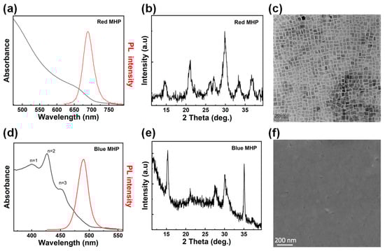
Figure 1.
(a) PL and absorbance spectra of Zn-CsPbI3 nanocrystal film. (b) XRD spectrum of Zn-CsPbI3 nanocrystal film. (c) TEM image of Zn-CsPbI3 nanocrystals. (d) PL and absorbance spectra of PEA2(Cs1-xEAxPbBr3)2PbBr4 film. (e) XRD spectrum of PEA2(Cs1-xEAxPbBr3)2PbBr4 film. (f) SEM image of PEA2(Cs1-xEAxPbBr3)2PbBr4 film.
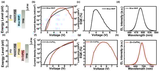
Figure 2.
(a,e) Energy level diagrams of blue and red PeLEDs. MHP: metal halide perovskite. (b) and (f) Current density and luminance versus voltage plots of blue and red PeLEDs. (c,g) EQE versus voltage plots of blue and red PeLEDs. (d,h) EL spectra of blue and red PeLEDs.
The orthogonality of the solvent needs to be considered in the preparation of the tandem device, and the light-emitting direction needs to avoid going from the blue-emitting layer to the red-emitting layer, which would result in a part of the blue light energy being absorbed and energy loss. Here, the tandem device structure is shown in Figure 3a; we use the polar solvent dimethyl sulfoxide (DMSO) to prepare the blue emission layer, which is located at the bottom of the device. The red quantum dots are dispersed in the non-polar solvent n-octane, which prevents damage to the blue emission layer during the spin coating process. Meanwhile, when the device is working, the light-emitting direction is from the red-emitting layer to blue-emitting layer, avoiding the energy loss caused by blue light absorption. We first chose organic/organic materials as the intermediate connector, as this structure has been proven to effectively modulate the transport and distribution of electrons and holes, resulting in spectrally stable devices [23]. We dissolved B3PYMPM and PTAA in chlorobenzene and spin-coated on the blue emission layer as an intermediate connector. As shown in Figure 3b, the turn-on voltage of the device is 6.8 V, and the device achieves a maximum luminance of 15 cd/m2 at 10.4 V. The maximum EQE is only 1.4% (Figure 3c), which is much lower than that of monochromatic devices. The higher turn-on voltage indicates that the energy level of the intermediate connector does not match the emission layer, while the low brightness of the device indicates that the intermediate connector has an inefficient charge generation/injection capability [33]. Figure 3d shows the EL spectra of the device from 7.2 V to 10.4 V. The EL peaks at 490 nm and 690 nm are consistent with monochromatic devices. As shown in Figure 3e, the Commission Internationale de l’Éclairage (CIE) coordinates corresponding to the EL spectra at different biases exhibit large deviations. The x value fluctuates between 0.22 and 0.29, and the y value fluctuates between 0.36 and 0.38. In addition, we carried out a storage stability test. The films were placed in a glove box for 7 days, after the spin-coated red quantum dot had been placed, then TPBi/LiF/Al was evaporated. The EL spectrum is shown in Figure 3f; the blue emission peak red-shifted from 490 nm to 512 nm, and the red emission peak blue-shifted from 690 nm to 673 nm. This indicates that the B3PYMPM/PTAA intermediate connector cannot suppress the halide migration, and Br ions and I ions diffuse from their respective emission layers.
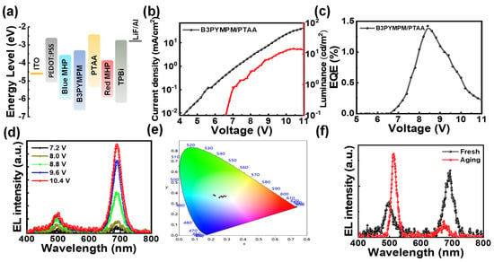
Figure 3.
(a) Energy level diagram of tandem PeLEDs. (b) Current density and luminance versus voltage plots of tandem PeLEDs. (c) EQE versus voltage plots of tandem PeLEDs. (d) EL spectra of tandem PeLEDs at different biases. (e) CIE coordinates. Each black dot corresponds to the spectra in (d). (f) The EL spectra of a fresh and an aging device.
In order to improve the ability of the intermediate connector to efficiently generate/inject charge and thus optimize the energy level structure, we used Al/HATCN/MoO3 to replace B3PYMPM/PTAA, and the energy level structure diagram is shown in Figure 4a. In this structure, carriers are generated at the interface of MoO3 and PTAA, and electrons can be efficiently transported from the valence band of PTAA to the conduction band of MoO3, and further transported to the conduction band of HATCN and Al under the bias, then injected into TPBi. Meanwhile, holes can be efficiently transported from MoO3 to PTAA [38]. As shown in Figure 4b, the turn-on voltage of the device drops to 6.2 V, compared to the higher turn-on voltage in the B3PYMPM/PTAA case. The maximum luminance is 58 cd/m2 at 13.6 V. The lower turn-on voltage indicates that the energy level of the intermediate connector matches well with the emission layer, while the higher brightness of the device indicates that the Al/HATCN/MoO3 has better charge generation/injection capabilities. As a result, the device achieves a maximum EQE of 8.5% (Figure 4c), which is the record EQE for all-perovskite EL white LEDs. The spectrum from 7.2 V to 10.4 V is shown in Figure 4d. Similarly, the EL peak position of the device is consistent with that of the monochromatic device. The inset shows an image of the white PeLED at an applied bias of 9.6 V, emitting bright and uniform white light. The CIE coordinates corresponding to the spectra at different biases are shown in Figure 4e, and the coordinate values fluctuate within a small range. The x values are between 0.31 and 0.34, and the y values are between 0.33 and 0.36. The Al/HATCN/MoO3 case exhibits more stable white emission, which indicates that the carrier distribution is more balanced after the replacement of the intermediate connector. Likewise, we performed spectral stability tests. As shown in Figure 4f, the spectral peak position of the device did not shift after 7 days, indicating that the organic-inorganic transport layer had successfully suppressed the diffusion of halide ions.
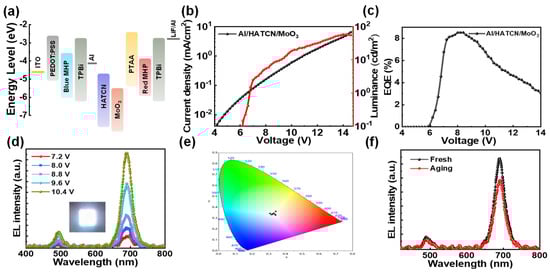
Figure 4.
(a) Energy level diagram of tandem PeLEDs. (b) Current density and luminance versus voltage plots of tandem PeLEDs. (c) EQ versus voltage plots of tandem PeLEDs. (d) EL spectra of tandem PeLEDs at different biases. Inset of panel (d): a photograph of the white PeLED. (e) CIE coordinates. Each black dot corresponds to the spectra in (d). (f) The EL spectra of a fresh and an aging device.
4. Conclusions
In summary, by adjusting the intermediate connector, we successfully improved the EQE of the tandem white PeLEDs from 1.4% to 8.5%. Compared with the organic hybrid transport layer, the organic-inorganic interconnecting layer has better charge generation/injection capabilities and energy level matching, thereby reducing the turn-on voltage. The distribution of carriers is more balanced, such that the spectra are more stable under different biases. In addition, this multilayer structure can also suppress the diffusion of halide ions more effectively. Nevertheless, we can see that the device under the Al/HATCN/MoO3 structure has a low brightness compared to the monochromatic device, and the EQE does not reach the sum of the EQEs of the monochromatic devices. Further work needs to be optimized in the selection of interlayer materials to further improve carrier transport and radiative recombination. We believe that this multilayer organic/inorganic structure will pave the way for the future development of efficient and stable all-perovskite white light devices.
Author Contributions
Conceptualization, Y.Y.; methodology, Y.Y. and Q.Z.; validation, Y.Y. and Q.Z.; investigation, Y.Y., Q.D. and R.T.; resources, Y.Y.; data curation, Z.W. and Y.Y.; writing—original draft preparation, Y.Y.; writing—review and editing, Y.Y., Q.Z., Z.W., Q.D., R.T. and X.W.; visualization, Q.D. and R.T.; supervision, Y.Y.; project administration, Y.Y.; and funding acquisition, Y.Y. All authors have read and agreed to the published version of the manuscript.
Funding
This research was funded by the National Natural Science Foundation of China (Grant No. 61904160, 12002312), the National Key Research and Development Program of China (No. 2020YFC2007101), the Natural Science Foundation of Zhejiang Province of China (Nos. LQ20A020005) and the Postdoctoral Program of Zhejiang Province.
Institutional Review Board Statement
Not applicable.
Informed Consent Statement
Not applicable.
Data Availability Statement
The data presented in this study are available upon request to the corresponding author.
Conflicts of Interest
The authors declare no conflict of interest.
References
- Joo, W.-J.; Kyoung, J.; Esfandyarpour, M.; Lee, S.-H.; Koo, H.; Song, S.; Kwon, Y.-N.; Song, S.H.; Bae, J.C.; Jo, A.; et al. Metasurface-driven OLED displays beyond 10,000 pixels per inch. Science 2020, 370, 459–463. [Google Scholar] [CrossRef]
- García de Arquer, F.P.; Talapin, D.V.; Klimov, V.I.; Arakawa, Y.; Bayer, M.; Sargent, E.H. Semiconductor quantum dots: Technological progress and future challenges. Science 2021, 373, eaaz8541. [Google Scholar] [CrossRef]
- Fakharuddin, A.; Gangishetty, M.K.; Abdi-Jalebi, M.; Chin, S.-H.; bin Yusoff, A.R.M.; Congreve, D.N.; Tress, W.; Deschler, F.; Vasilopoulou, M.; Bolink, H.J. Perovskite light-emitting diodes. Nat. Electron. 2022, 5, 203–216. [Google Scholar] [CrossRef]
- Xuan, T.; Guo, S.; Bai, W.; Zhou, T.; Wang, L.; Xie, R.-J. Ultrastable and highly efficient green-emitting perovskite quantum dot composites for Mini-LED displays or backlights. Nano Energy 2022, 95, 107003. [Google Scholar] [CrossRef]
- Wei, C.; Su, W.; Li, J.; Xu, B.; Shan, Q.; Wu, Y.; Zhang, F.; Luo, M.; Xiang, H.; Cui, Z.; et al. A Universal Ternary-Solvent-Ink Strategy toward Efficient Inkjet-Printed Perovskite Quantum Dot Light-Emitting Diodes. Adv. Mater. 2022, 34, 2107798. [Google Scholar] [CrossRef] [PubMed]
- Righetto, M.; Meggiolaro, D.; Rizzo, A.; Sorrentino, R.; He, Z.; Meneghesso, G.; Sum, T.C.; Gatti, T.; Lamberti, F. Coupling Halide Perovskites with Different Materials: From Doping to Nanocomposites, beyond Photovoltaics. Prog. Mater. Sci. 2020, 110, 100639. [Google Scholar] [CrossRef]
- Chen, N.; Bai, Z.; Wang, Z.; Ji, H.; Liu, R.; Cao, C.; Wang, H.; Jiang, F.; Zhong, H. Low Cost Perovskite Quantum Dots Film Based Wide Color Gamut Backlight Unit for LCD TVs. SID Symp. Dig. Tech. Pap. 2018, 49, 1657–1659. [Google Scholar] [CrossRef]
- Shamsi, J.; Rainò, G.; Kovalenko, M.V.; Stranks, S.D. To nano or not to nano for bright halide perovskite emitters. Nat. Nanotechnol. 2021, 16, 1164–1168. [Google Scholar] [CrossRef] [PubMed]
- Ko, J.; Ma, K.; Joung, J.F.; Park, S.; Bang, J. Ligand-Assisted Direct Photolithography of Perovskite Nanocrystals Encapsulated with Multifunctional Polymer Ligands for Stable, Full-Colored, High-Resolution Displays. Nano Lett. 2021, 21, 2288–2295. [Google Scholar] [CrossRef]
- Brenner, T.M.; Egger, D.A.; Kronik, L.; Hodes, G.; Cahen, D. Hybrid organic-inorganic perovskites: Low-cost semiconductors with intriguing charge-transport properties. Nat. Rev. Mater. 2016, 1, 15007. [Google Scholar] [CrossRef]
- Nedelcu, G.; Protesescu, L.; Yakunin, S.; Bodnarchuk, M.I.; Grotevent, M.J.; Kovalenko, M.V. Fast Anion-Exchange in Highly Luminescent Nanocrystals of Cesium Lead Halide Perovskites (CsPbX3, X = Cl, Br, I). Nano Lett. 2015, 15, 5635–5640. [Google Scholar] [CrossRef]
- Voznyy, O.; Sutherland, B.R.; Ip, A.H.; Zhitomirsky, D.; Sargent, E.H. Engineering charge transport by heterostructuring solution-processed semiconductors. Nat. Rev. Mater. 2017, 2, 17026. [Google Scholar] [CrossRef]
- Lu, M.; Zhang, Y.; Wang, S.; Guo, J.; Yu, W.W.; Rogach, A.L. Metal Halide Perovskite Light-Emitting Devices: Promising Technology for Next-Generation Displays. Adv. Funct. Mater. 2019, 29, 1902008. [Google Scholar] [CrossRef]
- Tan, Z.-K.; Moghaddam, R.S.; Lai, M.L.; Docampo, P.; Higler, R.; Deschler, F.; Price, M.; Sadhanala, A.; Pazos, L.M.; Credgington, D.; et al. Bright light-emitting diodes based on organometal halide perovskite. Nat. Nanotechnol. 2014, 9, 687–692. [Google Scholar] [CrossRef] [PubMed]
- Zhu, L.; Cao, H.; Xue, C.; Zhang, H.; Qin, M.; Wang, J.; Wen, K.; Fu, Z.; Jiang, T.; Xu, L.; et al. Unveiling the additive-assisted oriented growth of perovskite crystallite for high performance light-emitting diodes. Nat. Commun. 2021, 12, 5081. [Google Scholar] [CrossRef]
- Liu, Z.; Qiu, W.; Peng, X.; Sun, G.; Liu, X.; Liu, D.; Li, Z.; He, F.; Shen, C.; Gu, Q.; et al. Perovskite Light-Emitting Diodes with EQE Exceeding 28% through a Synergetic Dual-Additive Strategy for Defect Passivation and Nanostructure Regulation. Adv. Mater. 2021, 33, 2103268. [Google Scholar] [CrossRef]
- Liu, Y.; Li, Z.; Xu, J.; Dong, Y.; Chen, B.; Park, S.M.; Ma, D.; Lee, S.; Huang, J.E.; Teale, S.; et al. Wide-Bandgap Perovskite Quantum Dots in Perovskite Matrix for Sky-Blue Light-Emitting Diodes. J. Am. Chem. Soc. 2022, 144, 4009–4016. [Google Scholar] [CrossRef]
- Chen, Z.; Li, Z.; Chen, Z.; Xia, R.; Zou, G.; Chu, L.; Su, S.-J.; Peng, J.; Yip, H.-L.; Cao, Y. Utilization of Trapped Optical Modes for White Perovskite Light-Emitting Diodes with Efficiency over 12%. Joule 2021, 5, 456–466. [Google Scholar] [CrossRef]
- Jamaludin, N.F.; Yantara, N.; Giovanni, D.; Febriansyah, B.; Tay, Y.B.; Salim, T.; Sum, T.C.; Mhaisalkar, S.; Mathews, N. White Electroluminescence from Perovskite–Organic Heterojunction. ACS Energy Lett. 2020, 5, 2690–2697. [Google Scholar] [CrossRef]
- Žukauskas, A.; Vaicekauskas, R.; Shur, M. Solid-state lamps with optimized color saturation ability. Opt. Express 2010, 18, 2287–2295. [Google Scholar] [CrossRef]
- Chen, J.; Xiang, H.; Wang, J.; Wang, R.; Li, Y.; Shan, Q.; Xu, X.; Dong, Y.; Wei, C.; Zeng, H. Perovskite White Light Emitting Diodes: Progress, Challenges, and Opportunities. ACS Nano 2021, 15, 17150–17174. [Google Scholar] [CrossRef] [PubMed]
- Chen, J.; Wang, J.; Xu, X.; Li, J.; Song, J.; Lan, S.; Liu, S.; Cai, B.; Han, B.; Precht, J.T.; et al. Efficient and bright white light-emitting diodes based on single-layer heterophase halide perovskites. Nat. Photonics 2021, 15, 238–244. [Google Scholar] [CrossRef]
- Mao, J.; Lin, H.; Ye, F.; Qin, M.; Burkhartsmeyer, J.M.; Zhang, H.; Lu, X.; Wong, K.S.; Choy, W.C.H. All-Perovskite Emission Architecture for White Light-Emitting Diodes. ACS Nano 2018, 12, 10486–10492. [Google Scholar] [CrossRef] [PubMed]
- Luo, J.; Wang, X.; Li, S.; Liu, J.; Guo, Y.; Niu, G.; Yao, L.; Fu, Y.; Gao, L.; Dong, Q.; et al. Efficient and stable emission of warm-white light from lead-free halide double perovskites. Nature 2018, 563, 541–545. [Google Scholar] [CrossRef]
- Dohner, E.R.; Jaffe, A.; Bradshaw, L.R.; Karunadasa, H.I. Intrinsic White-Light Emission from Layered Hybrid Perovskites. J. Am. Chem. Soc. 2014, 136, 13154–13157. [Google Scholar] [CrossRef]
- Cai, P.; Wang, X.; Seo, H.J.; Yan, X. Bluish-white-light-emitting diodes based on two-dimensional lead halide perovskite (C6H5C2H4NH3)2PbCl2Br2. Appl. Phys. Lett. 2018, 112, 153901. [Google Scholar] [CrossRef]
- Mao, L.; Guo, P.; Kepenekian, M.; Hadar, I.; Katan, C.; Even, J.; Schaller, R.D.; Stoumpos, C.C.; Kanatzidis, M.G. Structural Diversity in White-Light-Emitting Hybrid Lead Bromide Perovskites. J. Am. Chem. Soc. 2018, 140, 13078–13088. [Google Scholar] [CrossRef]
- Chen, H.; Zhu, L.; Xue, C.; Liu, P.; Du, X.; Wen, K.; Zhang, H.; Xu, L.; Xiang, C.; Lin, C.; et al. Efficient and bright warm-white electroluminescence from lead-free metal halides. Nat. Commun. 2021, 12, 1421. [Google Scholar] [CrossRef]
- Ma, Z.; Shi, Z.; Yang, D.; Li, Y.; Zhang, F.; Wang, L.; Chen, X.; Wu, D.; Tian, Y.; Zhang, Y.; et al. High Color-Rendering Index and Stable White Light-Emitting Diodes by Assembling Two Broadband Emissive Self-Trapped Excitons. Adv. Mater. 2021, 33, 2001367. [Google Scholar] [CrossRef]
- Yu, H.; Wang, H.; Pozina, G.; Yin, C.; Liu, X.-K.; Gao, F. Single-emissive-layer all-perovskite white light-emitting diodes employing segregated mixed halide perovskite crystals. Chem. Sci. 2020, 11, 11338–11343. [Google Scholar] [CrossRef]
- Chang, C.-Y.; Solodukhin, A.N.; Liao, S.-Y.; Mahesh, K.P.O.; Hsu, C.-L.; Ponomarenko, S.A.; Luponosov, Y.N.; Chao, Y.-C. Perovskite white light-emitting diodes based on a molecular blend perovskite emissive layer. J. Mater. Chem. C 2019, 7, 8634–8642. [Google Scholar] [CrossRef]
- Fung, M.-K.; Li, Y.-Q.; Liao, L.-S. Tandem Organic Light-Emitting Diodes. Adv. Mater. 2016, 28, 10381–10408. [Google Scholar] [CrossRef] [PubMed]
- Zhang, H.; Chen, S.; Sun, X.W. Efficient Red/Green/Blue Tandem Quantum-Dot Light-Emitting Diodes with External Quantum Efficiency Exceeding 21%. ACS Nano 2018, 12, 697–704. [Google Scholar] [CrossRef] [PubMed]
- Zhang, H.; Su, Q.; Sun, Y.; Chen, S. Efficient and Color Stable White Quantum-Dot Light-Emitting Diodes with External Quantum Efficiency Over 23%. Adv. Opt. Mater. 2018, 6, 1800354. [Google Scholar] [CrossRef]
- Jeong, S.-H.; Park, J.; Han, T.-H.; Zhang, F.; Zhu, K.; Kim, J.S.; Park, M.-H.; Reese, M.O.; Yoo, S.; Lee, T.-W. Characterizing the Efficiency of Perovskite Solar Cells and Light-Emitting Diodes. Joule 2020, 4, 1206–1235. [Google Scholar] [CrossRef]
- Jin, W.; Deng, Y.; Guo, B.; Lian, Y.; Zhao, B.; Di, D.; Sun, X.; Wang, K.; Chen, S.; Yang, Y.; et al. On the accurate characterization of quantum-dot light-emitting diodes for display applications. NPJ Flex. Electron. 2022, 6, 35. [Google Scholar] [CrossRef]
- Chu, Z.; Zhao, Y.; Ma, F.; Zhang, C.-X.; Deng, H.; Gao, F.; Ye, Q.; Meng, J.; Yin, Z.; Zhang, X.; et al. Large Cation Ethylammonium Incorporated Perovskite for Efficient and Spectra Stable Blue Light-Emitting Diodes. Nat. Commun. 2020, 11, 4165. [Google Scholar] [CrossRef]
- Shen, X.; Zhang, Y.; Kershaw, S.V.; Li, T.; Wang, C.; Zhang, X.; Wang, W.; Li, D.; Wang, Y.; Lu, M.; et al. Zn-Alloyed CsPbI3 Nanocrystals for Highly Efficient Perovskite Light-Emitting Devices. Nano Lett. 2019, 19, 1552–1559. [Google Scholar] [CrossRef]
Publisher’s Note: MDPI stays neutral with regard to jurisdictional claims in published maps and institutional affiliations. |
© 2022 by the authors. Licensee MDPI, Basel, Switzerland. This article is an open access article distributed under the terms and conditions of the Creative Commons Attribution (CC BY) license (https://creativecommons.org/licenses/by/4.0/).